EP0932988B1 - Allongement de la duree de vie des accumulateurs dans un appareil electronique - Google Patents
Allongement de la duree de vie des accumulateurs dans un appareil electronique Download PDFInfo
- Publication number
- EP0932988B1 EP0932988B1 EP98912643A EP98912643A EP0932988B1 EP 0932988 B1 EP0932988 B1 EP 0932988B1 EP 98912643 A EP98912643 A EP 98912643A EP 98912643 A EP98912643 A EP 98912643A EP 0932988 B1 EP0932988 B1 EP 0932988B1
- Authority
- EP
- European Patent Office
- Prior art keywords
- voltage
- battery
- coupled
- terminal
- multiplying
- Prior art date
- Legal status (The legal status is an assumption and is not a legal conclusion. Google has not performed a legal analysis and makes no representation as to the accuracy of the status listed.)
- Expired - Lifetime
Links
Images
Classifications
-
- H—ELECTRICITY
- H04—ELECTRIC COMMUNICATION TECHNIQUE
- H04B—TRANSMISSION
- H04B1/00—Details of transmission systems, not covered by a single one of groups H04B3/00 - H04B13/00; Details of transmission systems not characterised by the medium used for transmission
- H04B1/06—Receivers
- H04B1/16—Circuits
- H04B1/1607—Supply circuits
-
- H—ELECTRICITY
- H02—GENERATION; CONVERSION OR DISTRIBUTION OF ELECTRIC POWER
- H02J—CIRCUIT ARRANGEMENTS OR SYSTEMS FOR SUPPLYING OR DISTRIBUTING ELECTRIC POWER; SYSTEMS FOR STORING ELECTRIC ENERGY
- H02J2207/00—Indexing scheme relating to details of circuit arrangements for charging or depolarising batteries or for supplying loads from batteries
- H02J2207/20—Charging or discharging characterised by the power electronics converter
Definitions
- the present invention relates to an electronic apparatus particularly, but not exclusively, to a radio apparatus fabricated from integrated circuits at least one of which operates at a different voltage to the others.
- a radio apparatus fabricated from integrated circuits at least one of which operates at a different voltage to the others.
- the present invention will be described with reference to a digital one-way pager.
- a one-way pager comprises a receiver IC, a decoder IC and a microprocessor IC together with one or more transducers and one or more push buttons providing a man-machine interface.
- the integrated circuits currently in use in pagers operate at various voltages in the range between 0.85 and 3.5 volts.
- the compactness of a one-way pager means that its power source is usually a single cell battery having a terminal voltage of 1.5 volts which is stepped up by a dc-dc converter say 3 volts.
- dc-dc converters have an efficiency of the order of 60 to 90% which reduces the effective life of the cell.
- GB2284085A discloses a selective call receiver having part of its circuitry powered by a battery and part by a DC/DC converter. It does not address the problem of powering the circuitry when the battery voltage falls.
- US5193212 discloses a circuit for saving battery power in a radio paging receiver by switching power on and off to selected portions of circuitry in response to reception of power saving signals. It does not address the problem of powering the circuitry when the battery voltage falls.
- An object of the present invention is to extend the useful life of a battery directly powering at least part of an overall electronic circuit for as long as possible.
- an electronic apparatus comprising means for receiving a battery, a first part, a second part, wherein the second part is designed to be operated at a voltage higher than that of the battery, and a voltage multiplying means for multiplying the battery voltage and for supplying it to the second part, characterised in that the first part is designed to be operated at the voltage of the battery when the voltage of the battery is equal to or above a predefined minimum voltage, and by control means for comparing a voltage representative of the battery voltage with a reference voltage and whenever the reference voltage is the greater, causing current to be supplied to the first part from the voltage multiplying means.
- the present invention is based on recognition of the fact that whenever possible power should be supplied directly by a battery cell to the first part but if the battery terminal voltage should drop, the current supply to the first part is replaced by current supplied from the multiplier to maintain full circuit operation and sensitivity. As a result the first part can remain fully operative whilst the terminal voltage of the cell has dropped below the predefined minimum voltage thus extending the useful life of the cell because the multiplier can operate successfully down to a lower minimum terminal voltage. Thus all the available battery capacity is used to power the electronic apparatus even though the battery voltage level has dropped below that at which at least parts of the apparatus would operate at.
- the voltage multiplying means may produce a regulated higher voltage and means may be provided for stepping down the regulated higher voltage for supply to the first part.
- the first part comprises an integrated radio receiver, such as a receiver for receiving paging signals
- the second part comprises at least a paging signal decoder.
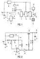
- the pager comprises an integrated receiver IC 10 having a signal input coupled to an antenna.
- a decoder IC 14 is coupled to an output of the receiver 10 and serves to decode the demodulated signals.
- a microcontroller IC 16 is coupled to the decoder IC 14 and serves to process signals produced by the decoder and to control various functions of the pager.
- the decoder is implemented using software in the microcontroller IC16 itself thus reducing the IC count:
- a switch pad 18 is coupled to the microcontroller IC 16 and serves as a man-machine interface.
- An acoustic transducer 20 is coupled to an output of the microcontroller IC 16 and serves to provide an audible alert in response to the receipt of a signal.
- Other annunciating devices not shown, including a LED light emitter and a vibrator may be provided.
- a LCD panel 22, including a driver, is coupled to another output of the microcontroller IC16.
- the receiver IC 10 can operate from a specified minimum voltage of 1.05V upwards to say 1.5V whereas the decoder IC 14 and microcontroller IC 16 operate at a higher voltage of the order of 3 volts.
- a single cell battery 24 providing a voltage V BAT of the order of 1.5 volts maximum is coupled to a voltage multiplier 26, for example a MAX 867, to a pole 28 of a single pole changeover switch 30 and to an input 32 of a voltage comparator circuit 34.
- a reference voltage Vr is applied to a second input 36 of the comparator 34 which provides an output 38 for controlling the switch 30.
- the value of Vr corresponds to the minimum operating voltage of the IC 10 as specified by the manufacturer in this instance 1.05 volts.
- the voltage multiplier 26 produces a regulated 3 volt output which is coupled to a second pole 42 of the switch 30 by way of a voltage stepping stage 40 and to the decoder IC 14 and the microcontroller IC 16.
- the voltage stepping stage 40 drops the voltage by approximately half to say 1.5 volts.
- the switch 30 In operation when the terminal voltage of the battery 24 is greater than Vr (1.05 volts), the switch 30 is controlled to couple the battery voltage on the terminal 28 to the receiver IC 10 which is able to operate with an acceptable sensitivity. If now there is a sudden demand on the battery power causing the terminal voltage of the battery to drop below the reference voltage Vr, the comparator 34 causes the switch 30 to change-over to the terminal 42 so that a stepped down version of the voltage output of the multiplier 26 is supplied to the receiver IC 10 to thereby maintain its sensitivity. The change-over of the switch 30 to the multiplier 26 output lasts for at least as long as the surge in demand lasts.
- the comparator 34 causes the switch 30 to be connected to the pole 42 so that the receiver IC 10 is powered via the multiplier 26 which is able to operate down to a V BAT which equals the lowest voltage possible for operation of the multiplier 26, that is, of the order of say 0.6V.
- FIG. 2 illustrates an embodiment of the comparator 34 and switch 30 which can be used in the circuit shown in Figure 1.
- the battery 24 is coupled to the emitter electrode of a common base connected PNP transistor 44 which functions as the switch 30.
- the collector electrode of the transistor 44 is coupled to a receiver power supply terminal 46.
- a capacitor 48 is provided in the receiver supply path to smooth out any ripples and other interferences, for convenience of illustration the capacitor 48 is shown connected to the terminal 46.
- a comparator 50 has a non-inverting input 52 connected to a junction 54 of a potential divider formed by resistors 56, 58 connected in series between a regulated 3V supply from the multiplier 26 and the battery terminal.
- the comparator 50 itself operates from the 3V supply.
- a reference voltage Vr which may be derived from the regulated voltage supply, is applied to an inverting input 60 of the comparator 50.
- the output of the comparator is coupled to an inverter 62, the input of which is coupled by way of a resistor 64 to the regulated voltage supply.
- the output of the inverter 62 is coupled by way of a resistor 66 to the base electrode of the transistor 44.
- a voltage step-down arrangement comprising series connected diodes 68, 70 is connected between the output of the inverter 62 and the terminal 46.
- the comparator 50 output is high which in turn means that the output of the inverter 62 is low.
- Transistor 44 is forward biassed and saturated so that substantially the full battery voltage V BAT is applied to the terminal 46.
- the output of the comparator 50 is low causing the output of the inverter 62 to go high.
- the transistor 44 is reverse biased effectively disconnecting the battery from the terminal 46.
- the series connected diodes 68, 70 steps down the 3 volts derived from the output of the inverter 62 to 1.5 volts which appears on the terminal 46. This will continued until the multiplier 26 can no longer operate as the battery voltage has decreased to below its minimum operating voltage.
- V BAT drops temporarily below 1.05V and the illustrated circuit operates dynamically to ensure that the receiver supply does not drop below 1.05V. In this way the receiver can operate efficiently while V BAT is above 1.05 volts and maintain operation, though less efficient, for lower battery voltage.
- the transistor 44 could be a field effect transistor (FET) with its source-drain path connected between the battery 24 and the terminal 46 and its gate electrode connected to the resistor 66.
- FET field effect transistor
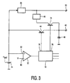
- Figure 3 shows an embodiment of the control circuit in which the microcontroller 16 monitors the output of the comparator 50 and provides the signals for controlling the switching of the dc power to the terminal 46.
- the voltage multiplier 26 the emitter electrode of PNP transistor 44 and the non-inverting input 52 of the comparator 50 are coupled to the positive terminal of the battery 24.
- a reference voltage Vr is applied to an inverting input 60 of the comparator.
- An output of the comparator 50 is coupled to the microcontroller 16.
- An output of the voltage multiplier 26 is coupled to a terminal 72 which is coupled to those circuit elements, such as the microcontroller 16, which require a supply voltage of say 3 volts and to the voltage stepping stage 40.
- An output of the stage 40 is coupled to an emitter electrode of another PNP transistor 74.
- Collector electrodes of the transistors 44, 74 are coupled to the terminal 46 for supplying a lower voltage required by other circuit elements, such as the receiver IC 10 ( Figure 1).
- Base electrodes of the transistors 44, 74 are connected to respective outputs 76, 78 of the micro-controller 16.
- the capacitor 48 is coupled to the terminal 46 to smooth any ripples and other interferences on the voltage supplied to that terminal.
- the state of the comparator's output is high so that the output 76 is High rendering the transistor 44 conductive and the output 78 is Low rendering the transistor 74 non-conductive. If V BAT drops below Vr, the state of the comparator's output changes to Low causing the outputs 76, 78 to change state to Low and High, respectively.
- Insodoing the current supplied to the terminal 46 is derived from the multiplier 26 by way of the voltage stepping stage 40 and the emitter - collector path of the transistor 74.
- the circuit changes back when V BAT is greater than Vr.
- the transistors 44, 74 may be NPN transistors or FETs.
- Electronic apparatus especially telecommunications apparatus such as pagers, cordless and cellular telephones.
Landscapes
- Engineering & Computer Science (AREA)
- Computer Networks & Wireless Communication (AREA)
- Signal Processing (AREA)
- Mobile Radio Communication Systems (AREA)
- Circuits Of Receivers In General (AREA)
Claims (7)
- Appareil électronique comprenant un moyen permettant de recevoir une batterie (24), une première partie (10), une deuxième partie (14, 16), dans lequel la deuxième partie (14, 16) est conçue pour fonctionner à une tension supérieure à celle de la batterie (24), et un moyen de multiplication de tension (26) pour multiplier la tension de la batterie et la fournir à la deuxième partie (14, 16), caractérisé en ce que la première partie (10) est conçue pour fonctionner à la tension de la batterie (24) lorsque la tension de la batterie est égale ou supérieure à une tension minimum prédéfinie, et par un moyen de commande (34) permettant de comparer une tension représentative de ,la tension de la batterie à une tension de référence et, chaque fois que la tension de référence est la plus élevée, faire que le courant soit fourni à la première partie (10) à partir du moyen de multiplication de tension (26).
- Appareil suivant la revendication 1, caractérisé en ce que le moyen de multiplication de tension (26) est à même de produire une tension supérieure régulée et en ce qu'un moyen (40) est prévu pour abaisser la tension supérieure régulée pour l'alimentation de la première partie (10).
- Appareil suivant la revendication 1, caractérisé en ce que la première partie (10) comprend un récepteur radio intégré.
- Appareil suivant la revendication 1, caractérisé en ce que la première partie (10) comprend un récepteur radio intégré et la deuxième partie (14,16) comprend au moins un décodeur de signaux d'appel de personnes (14).
- Appareil suivant la revendication 1, caractérisé en ce que le moyen de commande (34) comprend un moyen de commutation à semi-conducteur (30) qui est polarisé dans le sens direct chaque fois que la tension représentative de la tension de la batterie est supérieure à la tension de référence et qui est polarisé dans le sens inverse chaque fois que la tension de référence est la plus élevée.
- Appareil suivant la revendication 1, caractérisé par un premier moyen de commutation (44) connecté entre le moyen de réception de batterie et la première partie (10), un deuxième moyen de commutation (74) connecté entre le moyen de multiplication de tension (26) et la première partie (10), dans lequel le moyen de commande (34) comprend un moyen de comparaison (50) pour comparer la tension de la batterie à une tension de référence et fournir un signal de commande de sortie indicatif du fait que la tension de la batterie dépasse la tension de référence et inversement, et un moyen logique (16) permettant de commander le premier et le deuxième moyens de commutation en réaction au signal de commande de sortie, de sorte que, chaque fois que le premier moyen de commutation (44) est passant, le deuxième moyen de commutation (74) est non passant et inversement.
- Appareil suivant la revendication 1, caractérisé en ce que le moyen (48) sert à lisser la tension à appliquer à ladite première partie (10).
Applications Claiming Priority (3)
| Application Number | Priority Date | Filing Date | Title |
|---|---|---|---|
| GBGB9716142.6A GB9716142D0 (en) | 1997-08-01 | 1997-08-01 | Extending battery life in electronic apparatus |
| GB9716142 | 1997-08-01 | ||
| PCT/IB1998/000576 WO1999007165A1 (fr) | 1997-08-01 | 1998-04-20 | Allongement de la duree de vie des accumulateurs dans un appareil electronique |
Publications (2)
| Publication Number | Publication Date |
|---|---|
| EP0932988A1 EP0932988A1 (fr) | 1999-08-04 |
| EP0932988B1 true EP0932988B1 (fr) | 2005-07-06 |
Family
ID=10816732
Family Applications (1)
| Application Number | Title | Priority Date | Filing Date |
|---|---|---|---|
| EP98912643A Expired - Lifetime EP0932988B1 (fr) | 1997-08-01 | 1998-04-20 | Allongement de la duree de vie des accumulateurs dans un appareil electronique |
Country Status (8)
| Country | Link |
|---|---|
| US (1) | US6028374A (fr) |
| EP (1) | EP0932988B1 (fr) |
| JP (1) | JP3952214B2 (fr) |
| KR (1) | KR100581604B1 (fr) |
| CN (1) | CN1154373C (fr) |
| DE (1) | DE69830783T2 (fr) |
| GB (1) | GB9716142D0 (fr) |
| WO (1) | WO1999007165A1 (fr) |
Families Citing this family (9)
| Publication number | Priority date | Publication date | Assignee | Title |
|---|---|---|---|---|
| US6128603A (en) * | 1997-09-09 | 2000-10-03 | Dent; Warren T. | Consumer-based system and method for managing and paying electronic billing statements |
| US6369553B1 (en) * | 2000-03-31 | 2002-04-09 | Intel Corporation | Method and an apparatus for adjusting voltage from a source |
| US7043419B2 (en) * | 2002-09-20 | 2006-05-09 | International Business Machines Corporation | Method and apparatus for publishing and monitoring entities providing services in a distributed data processing system |
| JP4965069B2 (ja) * | 2004-10-21 | 2012-07-04 | ラピスセミコンダクタ株式会社 | 半導体集積回路 |
| US7782018B2 (en) * | 2007-09-10 | 2010-08-24 | Maxim Integrated Products, Inc. | Adaptive current limiting for any power source with output equivalent series resistance |
| US8805455B2 (en) | 2009-06-22 | 2014-08-12 | Motorola Solutions, Inc. | Method and apparatus for intrinsically safe operation of a communication device |
| US8320141B2 (en) * | 2009-08-05 | 2012-11-27 | Apple Inc. | High-efficiency, switched-capacitor power conversion using a resonant clocking circuit to produce gate drive signals for switching capacitors |
| US8933665B2 (en) | 2009-08-05 | 2015-01-13 | Apple Inc. | Balancing voltages between battery banks |
| CN102564604A (zh) * | 2010-12-09 | 2012-07-11 | 洁利来(福建)感应设备有限公司 | 一种电池使用寿命长的红外感应器及其控制方法 |
Family Cites Families (6)
| Publication number | Priority date | Publication date | Assignee | Title |
|---|---|---|---|---|
| US4560887A (en) * | 1983-12-22 | 1985-12-24 | Northern Telecom Limited | Standby power supply |
| KR910009665B1 (ko) * | 1989-05-31 | 1991-11-25 | 삼성전자 주식회사 | 무선 수신기의 전원 절약회로 및 그 제어방법 |
| TW198782B (fr) * | 1991-11-26 | 1993-01-21 | Samsung Electronics Co Ltd | |
| US5399956A (en) * | 1992-02-03 | 1995-03-21 | Motorola, Inc. | Backup battery system for a portable electronic device |
| US5448756A (en) * | 1992-07-02 | 1995-09-05 | Motorola, Inc. | High frequency battery saver for a radio receiver |
| JP3105718B2 (ja) * | 1993-11-19 | 2000-11-06 | 日本電気株式会社 | 個別選択呼出受信機 |
-
1997
- 1997-08-01 GB GBGB9716142.6A patent/GB9716142D0/en active Pending
-
1998
- 1998-04-20 WO PCT/IB1998/000576 patent/WO1999007165A1/fr active IP Right Grant
- 1998-04-20 DE DE69830783T patent/DE69830783T2/de not_active Expired - Lifetime
- 1998-04-20 EP EP98912643A patent/EP0932988B1/fr not_active Expired - Lifetime
- 1998-04-20 CN CNB988014009A patent/CN1154373C/zh not_active Expired - Lifetime
- 1998-04-20 KR KR1019997002727A patent/KR100581604B1/ko not_active IP Right Cessation
- 1998-04-20 JP JP52941298A patent/JP3952214B2/ja not_active Expired - Lifetime
- 1998-07-23 US US09/121,578 patent/US6028374A/en not_active Expired - Lifetime
Also Published As
| Publication number | Publication date |
|---|---|
| GB9716142D0 (en) | 1997-10-08 |
| JP2001506479A (ja) | 2001-05-15 |
| DE69830783D1 (de) | 2005-08-11 |
| WO1999007165A1 (fr) | 1999-02-11 |
| CN1154373C (zh) | 2004-06-16 |
| CN1241341A (zh) | 2000-01-12 |
| US6028374A (en) | 2000-02-22 |
| KR20000068673A (ko) | 2000-11-25 |
| EP0932988A1 (fr) | 1999-08-04 |
| JP3952214B2 (ja) | 2007-08-01 |
| KR100581604B1 (ko) | 2006-05-22 |
| DE69830783T2 (de) | 2006-05-18 |
Similar Documents
| Publication | Publication Date | Title |
|---|---|---|
| US5387820A (en) | Power supply circuit | |
| JP3294945B2 (ja) | 電源電圧調整回路とそれを用いた電子装置 | |
| US5130634A (en) | Battery charger for a portable wireless telephone set having means for tricklingly charging the battery with an increased current during a stand-by period of the telephone set | |
| EP0932988B1 (fr) | Allongement de la duree de vie des accumulateurs dans un appareil electronique | |
| JPH04211528A (ja) | 無線選択呼出受信機 | |
| US6476587B2 (en) | Power circuit, power circuit control method and electronic device using the power circuit | |
| CN1055632A (zh) | 自供电式基地和远方电话通信设备 | |
| US5606740A (en) | Time delay controlled switching for a DC/DC converter in a selective call device for reducing ripple | |
| US7512821B2 (en) | Power supply system and method for supplying power to CPU providing power saving mode | |
| KR100260499B1 (ko) | 진동 표시기와 접속하기 위한 선택 호출 수신기의 구조 | |
| JP2003514491A (ja) | バッテリの放電を制御する方法及び回路 | |
| JPH10327575A (ja) | 電源回路 | |
| US20050221871A1 (en) | Circuit and method for saving power of a mobile communication terminal | |
| JPH09181799A (ja) | 携帯電話機 | |
| US7047049B2 (en) | Radio communications device including at least one light source | |
| JPH0518491B2 (fr) | ||
| JP3716255B2 (ja) | 降圧dc−dcコンバータおよび端末装置 | |
| JP3153137B2 (ja) | ラジオ受信機 | |
| KR0183605B1 (ko) | 발진방지 회로를 구비한 카오디오 | |
| KR100236645B1 (ko) | 마이콤을 이용한 정전압 회로 | |
| EP0342049A2 (fr) | Circuit de commande d'alimentation pour équipement de véhicule | |
| JP2002078324A (ja) | Dc−dcコンバータ | |
| JP2563149Y2 (ja) | 充電装置 | |
| JPH11215699A (ja) | 携帯型電子機器 | |
| JP2989474B2 (ja) | コードレス電話機のオンフック検出装置 |
Legal Events
| Date | Code | Title | Description |
|---|---|---|---|
| PUAI | Public reference made under article 153(3) epc to a published international application that has entered the european phase |
Free format text: ORIGINAL CODE: 0009012 |
|
| AK | Designated contracting states |
Kind code of ref document: A1 Designated state(s): DE FR GB |
|
| 17P | Request for examination filed |
Effective date: 19990811 |
|
| 17Q | First examination report despatched |
Effective date: 20031204 |
|
| GRAP | Despatch of communication of intention to grant a patent |
Free format text: ORIGINAL CODE: EPIDOSNIGR1 |
|
| GRAS | Grant fee paid |
Free format text: ORIGINAL CODE: EPIDOSNIGR3 |
|
| GRAA | (expected) grant |
Free format text: ORIGINAL CODE: 0009210 |
|
| AK | Designated contracting states |
Kind code of ref document: B1 Designated state(s): DE FR GB |
|
| REG | Reference to a national code |
Ref country code: GB Ref legal event code: FG4D |
|
| REF | Corresponds to: |
Ref document number: 69830783 Country of ref document: DE Date of ref document: 20050811 Kind code of ref document: P |
|
| ET | Fr: translation filed | ||
| PLBE | No opposition filed within time limit |
Free format text: ORIGINAL CODE: 0009261 |
|
| STAA | Information on the status of an ep patent application or granted ep patent |
Free format text: STATUS: NO OPPOSITION FILED WITHIN TIME LIMIT |
|
| 26N | No opposition filed |
Effective date: 20060407 |
|
| REG | Reference to a national code |
Ref country code: GB Ref legal event code: 732E |
|
| REG | Reference to a national code |
Ref country code: FR Ref legal event code: TP |
|
| PGFP | Annual fee paid to national office [announced via postgrant information from national office to epo] |
Ref country code: FR Payment date: 20120522 Year of fee payment: 15 |
|
| REG | Reference to a national code |
Ref country code: FR Ref legal event code: ST Effective date: 20131231 |
|
| PG25 | Lapsed in a contracting state [announced via postgrant information from national office to epo] |
Ref country code: FR Free format text: LAPSE BECAUSE OF NON-PAYMENT OF DUE FEES Effective date: 20130430 |
|
| REG | Reference to a national code |
Ref country code: DE Ref legal event code: R082 Ref document number: 69830783 Country of ref document: DE Representative=s name: GRUENECKER PATENT- UND RECHTSANWAELTE PARTG MB, DE Ref country code: DE Ref legal event code: R081 Ref document number: 69830783 Country of ref document: DE Owner name: OCT CIRCUIT TECHNOLOGIES INTERNATIONAL LTD., IE Free format text: FORMER OWNER: NXP B.V., EINDHOVEN, NL |
|
| PGFP | Annual fee paid to national office [announced via postgrant information from national office to epo] |
Ref country code: GB Payment date: 20170324 Year of fee payment: 20 |
|
| PGFP | Annual fee paid to national office [announced via postgrant information from national office to epo] |
Ref country code: DE Payment date: 20170321 Year of fee payment: 20 |
|
| REG | Reference to a national code |
Ref country code: DE Ref legal event code: R071 Ref document number: 69830783 Country of ref document: DE |
|
| REG | Reference to a national code |
Ref country code: GB Ref legal event code: PE20 Expiry date: 20180419 |
|
| PG25 | Lapsed in a contracting state [announced via postgrant information from national office to epo] |
Ref country code: GB Free format text: LAPSE BECAUSE OF EXPIRATION OF PROTECTION Effective date: 20180419 |