EP0932137B1 - Display - Google Patents
Display Download PDFInfo
- Publication number
- EP0932137B1 EP0932137B1 EP98929803A EP98929803A EP0932137B1 EP 0932137 B1 EP0932137 B1 EP 0932137B1 EP 98929803 A EP98929803 A EP 98929803A EP 98929803 A EP98929803 A EP 98929803A EP 0932137 B1 EP0932137 B1 EP 0932137B1
- Authority
- EP
- European Patent Office
- Prior art keywords
- bank
- sig
- lines
- gate
- data lines
- Prior art date
- Legal status (The legal status is an assumption and is not a legal conclusion. Google has not performed a legal analysis and makes no representation as to the accuracy of the status listed.)
- Expired - Lifetime
Links
- 239000010408 film Substances 0.000 claims description 134
- 239000004065 semiconductor Substances 0.000 claims description 63
- 239000003990 capacitor Substances 0.000 claims description 38
- 239000000758 substrate Substances 0.000 claims description 28
- 238000000034 method Methods 0.000 claims description 21
- 239000011159 matrix material Substances 0.000 claims description 17
- 239000010409 thin film Substances 0.000 claims description 17
- 239000000463 material Substances 0.000 claims description 6
- 230000002940 repellent Effects 0.000 claims description 5
- 239000005871 repellent Substances 0.000 claims description 5
- XLYOFNOQVPJJNP-UHFFFAOYSA-N water Substances O XLYOFNOQVPJJNP-UHFFFAOYSA-N 0.000 claims description 5
- 239000010410 layer Substances 0.000 description 93
- 239000011229 interlayer Substances 0.000 description 19
- 238000002347 injection Methods 0.000 description 16
- 239000007924 injection Substances 0.000 description 16
- 230000003071 parasitic effect Effects 0.000 description 15
- 241000581364 Clinitrachus argentatus Species 0.000 description 12
- 230000009467 reduction Effects 0.000 description 9
- XUIMIQQOPSSXEZ-UHFFFAOYSA-N Silicon Chemical compound [Si] XUIMIQQOPSSXEZ-UHFFFAOYSA-N 0.000 description 7
- 238000010586 diagram Methods 0.000 description 7
- 229910052710 silicon Inorganic materials 0.000 description 7
- 239000010703 silicon Substances 0.000 description 7
- 238000010276 construction Methods 0.000 description 5
- BOTDANWDWHJENH-UHFFFAOYSA-N Tetraethyl orthosilicate Chemical compound CCO[Si](OCC)(OCC)OCC BOTDANWDWHJENH-UHFFFAOYSA-N 0.000 description 4
- 239000012535 impurity Substances 0.000 description 4
- 239000004973 liquid crystal related substance Substances 0.000 description 4
- 230000006872 improvement Effects 0.000 description 3
- 239000011344 liquid material Substances 0.000 description 3
- 238000004519 manufacturing process Methods 0.000 description 3
- 238000005192 partition Methods 0.000 description 3
- 230000002093 peripheral effect Effects 0.000 description 3
- 238000005268 plasma chemical vapour deposition Methods 0.000 description 3
- 239000002243 precursor Substances 0.000 description 3
- 230000008569 process Effects 0.000 description 3
- VYPSYNLAJGMNEJ-UHFFFAOYSA-N Silicium dioxide Chemical compound O=[Si]=O VYPSYNLAJGMNEJ-UHFFFAOYSA-N 0.000 description 2
- 229910052782 aluminium Inorganic materials 0.000 description 2
- XAGFODPZIPBFFR-UHFFFAOYSA-N aluminium Chemical compound [Al] XAGFODPZIPBFFR-UHFFFAOYSA-N 0.000 description 2
- 229910021417 amorphous silicon Inorganic materials 0.000 description 2
- QVGXLLKOCUKJST-UHFFFAOYSA-N atomic oxygen Chemical compound [O] QVGXLLKOCUKJST-UHFFFAOYSA-N 0.000 description 2
- 239000007789 gas Substances 0.000 description 2
- 238000005224 laser annealing Methods 0.000 description 2
- 229910052751 metal Inorganic materials 0.000 description 2
- 239000002184 metal Substances 0.000 description 2
- 229910052760 oxygen Inorganic materials 0.000 description 2
- 239000001301 oxygen Substances 0.000 description 2
- 229910021420 polycrystalline silicon Inorganic materials 0.000 description 2
- 229920005591 polysilicon Polymers 0.000 description 2
- 230000001681 protective effect Effects 0.000 description 2
- 229910052814 silicon oxide Inorganic materials 0.000 description 2
- 238000012360 testing method Methods 0.000 description 2
- OYPRJOBELJOOCE-UHFFFAOYSA-N Calcium Chemical compound [Ca] OYPRJOBELJOOCE-UHFFFAOYSA-N 0.000 description 1
- WHXSMMKQMYFTQS-UHFFFAOYSA-N Lithium Chemical compound [Li] WHXSMMKQMYFTQS-UHFFFAOYSA-N 0.000 description 1
- ZOKXTWBITQBERF-UHFFFAOYSA-N Molybdenum Chemical compound [Mo] ZOKXTWBITQBERF-UHFFFAOYSA-N 0.000 description 1
- 229910052581 Si3N4 Inorganic materials 0.000 description 1
- RTAQQCXQSZGOHL-UHFFFAOYSA-N Titanium Chemical compound [Ti] RTAQQCXQSZGOHL-UHFFFAOYSA-N 0.000 description 1
- 230000015572 biosynthetic process Effects 0.000 description 1
- 229910052791 calcium Inorganic materials 0.000 description 1
- 239000011575 calcium Substances 0.000 description 1
- 230000015556 catabolic process Effects 0.000 description 1
- 239000011248 coating agent Substances 0.000 description 1
- 238000000576 coating method Methods 0.000 description 1
- 230000000295 complement effect Effects 0.000 description 1
- 238000007796 conventional method Methods 0.000 description 1
- 230000007423 decrease Effects 0.000 description 1
- 238000006731 degradation reaction Methods 0.000 description 1
- 229910052744 lithium Inorganic materials 0.000 description 1
- 230000007246 mechanism Effects 0.000 description 1
- 230000004048 modification Effects 0.000 description 1
- 238000012986 modification Methods 0.000 description 1
- 229910052750 molybdenum Inorganic materials 0.000 description 1
- 239000011733 molybdenum Substances 0.000 description 1
- 229910052698 phosphorus Inorganic materials 0.000 description 1
- 239000011574 phosphorus Substances 0.000 description 1
- -1 phosphorus ions Chemical class 0.000 description 1
- 238000012545 processing Methods 0.000 description 1
- HQVNEWCFYHHQES-UHFFFAOYSA-N silicon nitride Chemical compound N12[Si]34N5[Si]62N3[Si]51N64 HQVNEWCFYHHQES-UHFFFAOYSA-N 0.000 description 1
- 239000007790 solid phase Substances 0.000 description 1
- 239000002904 solvent Substances 0.000 description 1
- 238000004544 sputter deposition Methods 0.000 description 1
- 229910052715 tantalum Inorganic materials 0.000 description 1
- GUVRBAGPIYLISA-UHFFFAOYSA-N tantalum atom Chemical compound [Ta] GUVRBAGPIYLISA-UHFFFAOYSA-N 0.000 description 1
- 229910052719 titanium Inorganic materials 0.000 description 1
- 239000010936 titanium Substances 0.000 description 1
- WFKWXMTUELFFGS-UHFFFAOYSA-N tungsten Chemical compound [W] WFKWXMTUELFFGS-UHFFFAOYSA-N 0.000 description 1
- 229910052721 tungsten Inorganic materials 0.000 description 1
- 239000010937 tungsten Substances 0.000 description 1
Images


Classifications
-
- G—PHYSICS
- G09—EDUCATION; CRYPTOGRAPHY; DISPLAY; ADVERTISING; SEALS
- G09F—DISPLAYING; ADVERTISING; SIGNS; LABELS OR NAME-PLATES; SEALS
- G09F9/00—Indicating arrangements for variable information in which the information is built-up on a support by selection or combination of individual elements
- G09F9/30—Indicating arrangements for variable information in which the information is built-up on a support by selection or combination of individual elements in which the desired character or characters are formed by combining individual elements
-
- G—PHYSICS
- G09—EDUCATION; CRYPTOGRAPHY; DISPLAY; ADVERTISING; SEALS
- G09G—ARRANGEMENTS OR CIRCUITS FOR CONTROL OF INDICATING DEVICES USING STATIC MEANS TO PRESENT VARIABLE INFORMATION
- G09G3/00—Control arrangements or circuits, of interest only in connection with visual indicators other than cathode-ray tubes
- G09G3/20—Control arrangements or circuits, of interest only in connection with visual indicators other than cathode-ray tubes for presentation of an assembly of a number of characters, e.g. a page, by composing the assembly by combination of individual elements arranged in a matrix no fixed position being assigned to or needed to be assigned to the individual characters or partial characters
- G09G3/22—Control arrangements or circuits, of interest only in connection with visual indicators other than cathode-ray tubes for presentation of an assembly of a number of characters, e.g. a page, by composing the assembly by combination of individual elements arranged in a matrix no fixed position being assigned to or needed to be assigned to the individual characters or partial characters using controlled light sources
- G09G3/30—Control arrangements or circuits, of interest only in connection with visual indicators other than cathode-ray tubes for presentation of an assembly of a number of characters, e.g. a page, by composing the assembly by combination of individual elements arranged in a matrix no fixed position being assigned to or needed to be assigned to the individual characters or partial characters using controlled light sources using electroluminescent panels
- G09G3/32—Control arrangements or circuits, of interest only in connection with visual indicators other than cathode-ray tubes for presentation of an assembly of a number of characters, e.g. a page, by composing the assembly by combination of individual elements arranged in a matrix no fixed position being assigned to or needed to be assigned to the individual characters or partial characters using controlled light sources using electroluminescent panels semiconductive, e.g. using light-emitting diodes [LED]
- G09G3/3208—Control arrangements or circuits, of interest only in connection with visual indicators other than cathode-ray tubes for presentation of an assembly of a number of characters, e.g. a page, by composing the assembly by combination of individual elements arranged in a matrix no fixed position being assigned to or needed to be assigned to the individual characters or partial characters using controlled light sources using electroluminescent panels semiconductive, e.g. using light-emitting diodes [LED] organic, e.g. using organic light-emitting diodes [OLED]
- G09G3/3225—Control arrangements or circuits, of interest only in connection with visual indicators other than cathode-ray tubes for presentation of an assembly of a number of characters, e.g. a page, by composing the assembly by combination of individual elements arranged in a matrix no fixed position being assigned to or needed to be assigned to the individual characters or partial characters using controlled light sources using electroluminescent panels semiconductive, e.g. using light-emitting diodes [LED] organic, e.g. using organic light-emitting diodes [OLED] using an active matrix
-
- H—ELECTRICITY
- H10—SEMICONDUCTOR DEVICES; ELECTRIC SOLID-STATE DEVICES NOT OTHERWISE PROVIDED FOR
- H10K—ORGANIC ELECTRIC SOLID-STATE DEVICES
- H10K59/00—Integrated devices, or assemblies of multiple devices, comprising at least one organic light-emitting element covered by group H10K50/00
- H10K59/10—OLED displays
- H10K59/12—Active-matrix OLED [AMOLED] displays
- H10K59/122—Pixel-defining structures or layers, e.g. banks
-
- H—ELECTRICITY
- H10—SEMICONDUCTOR DEVICES; ELECTRIC SOLID-STATE DEVICES NOT OTHERWISE PROVIDED FOR
- H10K—ORGANIC ELECTRIC SOLID-STATE DEVICES
- H10K59/00—Integrated devices, or assemblies of multiple devices, comprising at least one organic light-emitting element covered by group H10K50/00
- H10K59/10—OLED displays
- H10K59/12—Active-matrix OLED [AMOLED] displays
- H10K59/131—Interconnections, e.g. wiring lines or terminals
-
- H—ELECTRICITY
- H10—SEMICONDUCTOR DEVICES; ELECTRIC SOLID-STATE DEVICES NOT OTHERWISE PROVIDED FOR
- H10K—ORGANIC ELECTRIC SOLID-STATE DEVICES
- H10K59/00—Integrated devices, or assemblies of multiple devices, comprising at least one organic light-emitting element covered by group H10K50/00
- H10K59/80—Constructional details
- H10K59/8791—Arrangements for improving contrast, e.g. preventing reflection of ambient light
- H10K59/8792—Arrangements for improving contrast, e.g. preventing reflection of ambient light comprising light absorbing layers, e.g. black layers
-
- G—PHYSICS
- G09—EDUCATION; CRYPTOGRAPHY; DISPLAY; ADVERTISING; SEALS
- G09G—ARRANGEMENTS OR CIRCUITS FOR CONTROL OF INDICATING DEVICES USING STATIC MEANS TO PRESENT VARIABLE INFORMATION
- G09G2300/00—Aspects of the constitution of display devices
- G09G2300/04—Structural and physical details of display devices
- G09G2300/0404—Matrix technologies
- G09G2300/0417—Special arrangements specific to the use of low carrier mobility technology
-
- G—PHYSICS
- G09—EDUCATION; CRYPTOGRAPHY; DISPLAY; ADVERTISING; SEALS
- G09G—ARRANGEMENTS OR CIRCUITS FOR CONTROL OF INDICATING DEVICES USING STATIC MEANS TO PRESENT VARIABLE INFORMATION
- G09G2300/00—Aspects of the constitution of display devices
- G09G2300/04—Structural and physical details of display devices
- G09G2300/0421—Structural details of the set of electrodes
- G09G2300/0426—Layout of electrodes and connections
-
- G—PHYSICS
- G09—EDUCATION; CRYPTOGRAPHY; DISPLAY; ADVERTISING; SEALS
- G09G—ARRANGEMENTS OR CIRCUITS FOR CONTROL OF INDICATING DEVICES USING STATIC MEANS TO PRESENT VARIABLE INFORMATION
- G09G2300/00—Aspects of the constitution of display devices
- G09G2300/04—Structural and physical details of display devices
- G09G2300/0439—Pixel structures
- G09G2300/0465—Improved aperture ratio, e.g. by size reduction of the pixel circuit, e.g. for improving the pixel density or the maximum displayable luminance or brightness
-
- G—PHYSICS
- G09—EDUCATION; CRYPTOGRAPHY; DISPLAY; ADVERTISING; SEALS
- G09G—ARRANGEMENTS OR CIRCUITS FOR CONTROL OF INDICATING DEVICES USING STATIC MEANS TO PRESENT VARIABLE INFORMATION
- G09G2300/00—Aspects of the constitution of display devices
- G09G2300/08—Active matrix structure, i.e. with use of active elements, inclusive of non-linear two terminal elements, in the pixels together with light emitting or modulating elements
- G09G2300/0809—Several active elements per pixel in active matrix panels
- G09G2300/0842—Several active elements per pixel in active matrix panels forming a memory circuit, e.g. a dynamic memory with one capacitor
-
- G—PHYSICS
- G09—EDUCATION; CRYPTOGRAPHY; DISPLAY; ADVERTISING; SEALS
- G09G—ARRANGEMENTS OR CIRCUITS FOR CONTROL OF INDICATING DEVICES USING STATIC MEANS TO PRESENT VARIABLE INFORMATION
- G09G2300/00—Aspects of the constitution of display devices
- G09G2300/08—Active matrix structure, i.e. with use of active elements, inclusive of non-linear two terminal elements, in the pixels together with light emitting or modulating elements
- G09G2300/0876—Supplementary capacities in pixels having special driving circuits and electrodes instead of being connected to common electrode or ground; Use of additional capacitively coupled compensation electrodes
-
- G—PHYSICS
- G09—EDUCATION; CRYPTOGRAPHY; DISPLAY; ADVERTISING; SEALS
- G09G—ARRANGEMENTS OR CIRCUITS FOR CONTROL OF INDICATING DEVICES USING STATIC MEANS TO PRESENT VARIABLE INFORMATION
- G09G2320/00—Control of display operating conditions
- G09G2320/02—Improving the quality of display appearance
- G09G2320/0209—Crosstalk reduction, i.e. to reduce direct or indirect influences of signals directed to a certain pixel of the displayed image on other pixels of said image, inclusive of influences affecting pixels in different frames or fields or sub-images which constitute a same image, e.g. left and right images of a stereoscopic display
-
- G—PHYSICS
- G09—EDUCATION; CRYPTOGRAPHY; DISPLAY; ADVERTISING; SEALS
- G09G—ARRANGEMENTS OR CIRCUITS FOR CONTROL OF INDICATING DEVICES USING STATIC MEANS TO PRESENT VARIABLE INFORMATION
- G09G3/00—Control arrangements or circuits, of interest only in connection with visual indicators other than cathode-ray tubes
- G09G3/006—Electronic inspection or testing of displays and display drivers, e.g. of LED or LCD displays
-
- H—ELECTRICITY
- H10—SEMICONDUCTOR DEVICES; ELECTRIC SOLID-STATE DEVICES NOT OTHERWISE PROVIDED FOR
- H10K—ORGANIC ELECTRIC SOLID-STATE DEVICES
- H10K2102/00—Constructional details relating to the organic devices covered by this subclass
- H10K2102/301—Details of OLEDs
- H10K2102/351—Thickness
-
- H—ELECTRICITY
- H10—SEMICONDUCTOR DEVICES; ELECTRIC SOLID-STATE DEVICES NOT OTHERWISE PROVIDED FOR
- H10K—ORGANIC ELECTRIC SOLID-STATE DEVICES
- H10K50/00—Organic light-emitting devices
- H10K50/80—Constructional details
- H10K50/86—Arrangements for improving contrast, e.g. preventing reflection of ambient light
- H10K50/865—Arrangements for improving contrast, e.g. preventing reflection of ambient light comprising light absorbing layers, e.g. light-blocking layers
-
- H—ELECTRICITY
- H10—SEMICONDUCTOR DEVICES; ELECTRIC SOLID-STATE DEVICES NOT OTHERWISE PROVIDED FOR
- H10K—ORGANIC ELECTRIC SOLID-STATE DEVICES
- H10K59/00—Integrated devices, or assemblies of multiple devices, comprising at least one organic light-emitting element covered by group H10K50/00
- H10K59/10—OLED displays
- H10K59/12—Active-matrix OLED [AMOLED] displays
- H10K59/121—Active-matrix OLED [AMOLED] displays characterised by the geometry or disposition of pixel elements
Definitions
- the present invention relates to an active matrix display device in which driving of luminescent elements such as LEDs (light emitting diodes) or EL (electroluminescent) elements which emits light when a driving current is passed through an organic semiconductor film is controlled by thin film transistors (hereinafter referred to as TFTs). More specifically, the present invention relates to a technique of optimizing the layout to improve the display performance.
- luminescent elements such as LEDs (light emitting diodes) or EL (electroluminescent) elements which emits light when a driving current is passed through an organic semiconductor film
- TFTs thin film transistors
- TFT-EL thin-film-transistor-electroluminescent
- European Patent Application No. 98937856.7 entitled “Active Matrix Display Device” discloses an active matrix display device in which parasitic capacitance or the like is suppressed by forming a thick insulating film around an organic semiconductor film and disconnection or the like does not occur in the opposing electrode formed on the upper layer of the thick insulating film.
- European Patent Application No. 98929802.1 entitled “Display Apparatus” discloses a display apparatus capable of improving display quality by expanding the light-omission area of pixels by improving the layout of pixels and common power feed lines formed on a substrate. Both above referenced applications are copending with this one.
- Fig. 13 is a block diagram illustrating an example of such an active matrix display device in which carrier injection type organic thin film EL elements are employed.
- the display device 1A shown in this figure includes various elements formed on a transparent substrate, such as a plurality of scanning lines “gate", a plurality of data lines “sig” extending in a direction crossing the direction in which the plurality of scanning lines “gate” extend, a plurality of common power supply lines “com” extending in a direction parallel to the data lines “sig”, and pixel regions located at respective intersections of the data lines "sig” and the scanning lines “gate”.
- a data line driving circuit 3 including a shift register, level shifters, video lines, and analog switches.
- Each pixel region 7 includes a first TFT 20 having a gate electrode to which a scanning signal is supplied via a scanning line, a holding capacitor “cap” for holding an image signal supplied from a data line "sig" through the first TFT 20, a second TFT 30 having a gate electrode to which the image signal held by the holding capacitor “cap” is supplied, and a luminescent element 40 into which a driving current flows when the luminescent element 40 is electrically connected to a common power supply line "com" via the second TFT 30.
- the first TFT 20 and the second TFT 30 are formed using two respective island-shaped semiconductor films wherein one of the source/drain regions of the second TFT 30 is electrically connected to an interconnecting electrode 35 via a contact hole formed in a first interlayer insulating film 51 and the interconnecting electrode 35 is electrically connected to a pixel electrode 41.
- a hole injection layer 42, an organic semiconductor film 43, and an opposite electrode "op" are provided at upper layers above the pixel electrodes 41.
- the opposite electrode "op" extends across the data lines "sig" and other lines over a plurality of pixel regions 7.
- the other one of the source/drain regions of the second TFT 30 is electrically connected to the common power supply line "com" via a contact hole.
- one of the source/drain regions is electrically connected to a potential sustaining electrode "st" which in turn is electrically connected to an extension 310 of the gate electrode 31.
- a semiconductor film 400 which is doped with an impurity so that it exhibits conductivity, is disposed below the extension 310 such that the semiconductor film 400 and the extension 310 face each other via a gate insulating film 50.
- a holding capacitor "cap” is formed with the extension 310, the gate insulating film 50, and the semiconductor film 400.
- the semiconductor film 400 is electrically connected to the common power supply line "com” via a contact hole formed in the first interlayer insulating film 51.
- the holding capacitor “cap” holds the image signal supplied from the data line “sig” via the first TFT 20 so that the gate electrode 31 of the second TFT 30 is maintained at a potential corresponding to the image signal even after the first TFT 20 is turned off.
- the driving current keeps flowing from the common power supply line "com” into the luminescent element 40 and thus the luminescent element 40 keeps emitting light.
- the opposite electrode "op” opposing the pixel electrodes 41 is formed on the same transparent substrate 10 on which the pixel electrodes 41 are formed, such that the opposite electrode “op” extends over the entire surface of the transparent substrate 10 or over the plurality of pixel regions 7, and thus there is only a second insulating film 52 between the opposite electrode "op” and the data lines "sig".
- the data lines "sig” have a large parasitic capacitance which causes the data lines "sig” to have a large load.
- the data line driving circuit 3 also has a problem of a large load caused by the large parasitic capacitance.
- the inventor of the present invention has developed a technique of forming an organic semiconductor film in a desired area by emitting a liquid material from an ink-jet head.
- the inventor has also developed a technique of defining an area where an organic semiconductor film is to be formed by surrounding the area by a bank layer so that the organic semiconductor film can be formed precisely in the defined area by means of the ink-jet technique without producing a part protruding outward from the defined area.
- the inventor presents a technique of solving the above-described problems using the above techniques.
- a display device comprising elements formed on a substrate, the elements including: a plurality of scanning lines; a plurality of data lines extending in a direction crossing the direction in which the scanning lines extend; a plurality of common power supply lines extending in a direction parallel to the data lines; and pixel regions formed in the shape of a matrix defined by the data lines and the scanning lines, each pixel region including: a first TFT having a gate electrode to which a scanning signal is supplied via one of the scanning lines; a holding capacitor for holding an image signal supplied from a corresponding data line via the first TFT; a second TFT having a gate electrode to which the image signal held by the holding capacitor is supplied; and a luminescent element including an organic semiconductor film formed between a pixel electrode provided in each pixel region and an opposite electrode extending across the data lines such that the opposite electrode faces the plurality of pixel electrodes, the luminescent element being adapted to emit light when the organic semiconductor film is driven by
- the opposite electrode is formed at least over the entire pixel regions or in the shape of stripes over a wide area, the opposite electrode faces the data lines. This can result in a large parasitic capacitance associated with each data line.
- the bank layer formed between the data lines and the opposite electrode prevents a large parasitic capacitance from occurring between the opposite electrode and the data lines. This results in a reduction in the load of the data line driving circuit. Therefore, it is possible to achieve a reduction in power consumption and an increase in the speed of displaying operation.
- a first driving circuit for outputting the image signal over the data lines or a second driving circuit for outputting the scanning signal over the scanning lines may be formed, together with the plurality of pixel regions, on the substrate. If such a driving circuit is formed at a location facing the opposite electrode, the interconnection layer formed in the driving circuit also has a large parasitic capacitance. In the present invention, to avoid such a problem, the driving circuit is covered with the bank layer so as to prevent the driving circuit from having such a large parasitic capacitance with respect to the opposite electrode. This results in a reduction in the load of the driving circuit. As a result, a reduction in power consumption and an increase in the speed of displaying operation are achieved.
- the organic semiconductor film may be a film formed, by means of an ink-jet technique, in areas surrounded by the bank layer, wherein the bank layer may be a water repellent film capable of preventing the organic semiconductor film from protruding outward from the above-described areas during the process of forming the organic semiconductor film by means of the ink-jet technique.
- the bank layer may be formed to a thickness as large as about 1 ⁇ m. In this case, to achieve a good partition wall, the organic semiconductor film is not necessarily required to be water repellent.
- each pixel electrode overlapping the corresponding first thin film transistor or second thin film transistor be also covered with the bank layer.
- the driving current flowing in such a particular area of the organic semiconductor film which makes no contribution to the display is herein referred to as an useless current.
- the bank layer is formed in those areas where an useless current otherwise would occur so that no useless current flows in the areas.
- the bank layer is preferably formed of a black resist film so that the bank layer also serves as a black matrix which results in an improvement in the displaying performance.
- the opposite electrode is formed at least over the entire pixel regions or into the shape of stripes over a wide area, and thus light reflected by the opposite electrode can cause degradation in the contrast.
- the above problem is avoided by forming the bank layer of the black resist serving as a black matrix, which also serves to prevent parasitic capacitance. That is, the bank layer blocks light reflected from the opposite electrode and thus the contrast is improved.
- the driving currents for driving the respective luminescent elements are passed through the common power supply lines and thus the magnitude of the current passed through each common power supply line is greater than that flowing through each data line. Therefore, in the present invention, it is desirable that the resistance of each common power supply line per unit length be smaller than the resistance of each data line per unit length so that the common power supply line has a large current capacity.
- the common power supply lines and the data lines are made of the same material and they have the same thickness, the common power supply lines preferably have a larger width than the data lines.
- pixel regions be disposed at both sides of each common power supply line such that they are supplied with the driving current via this common power supply line, and furthermore, the data lines extend over the pixel regions on the sides opposite to the common power supply line. That is, elements are disposed into a pattern periodically repeated in the direction along the scanning lines wherein the unit pattern consists of a data line, pixels connected to that data line, a common power supply line, pixels connected to that common power supply line, and a data line supplying an image signal to those pixels.
- the unit pattern consists of a data line, pixels connected to that data line, a common power supply line, pixels connected to that common power supply line, and a data line supplying an image signal to those pixels.
- the unit pattern consists of a data line, pixels connected to that data line, a common power supply line, pixels connected to that common power supply line, and a data line supplying an image signal to those pixels.
- the unit pattern consists of a data line, pixels connected to that data line, a common power supply line, pixels connected
- an interconnection layer is preferably formed between these two data lines.
- the crosstalk can be prevented simply by maintaining the interconnection layer at a constant voltage at least for one horizontal scanning period.
- the center-to-center pitch of the organic semiconductor film areas be equal in any pixel regions arranged in the direction in which the scanning lines extend.
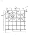
- Fig. 1 is a block diagram schematically illustrating the general layout of a display device.
- a display area 2 is formed in the center of the surface of a transparent substrate 10 serving as a base member of the display device.
- a data line driving circuit 3 (first driving circuit) for outputting an image signal and a test circuit 5 are formed on respective sides at ends of data lines "sig”
- scanning line driving circuits 4 (second driving circuits) for outputting a scanning signal are formed on respective sides at both ends of scanning lines ("gate").
- a shift register, level shifters, and analog switches are formed using complementary TFTs each consisting of an n-type TFT and a p-type TFT.
- mounting pads 6 serving as terminals for inputting an image signal, various voltages, and a pulse signal.
- various elements are formed on the transparent substrate 10. They include a plurality of scanning lines "gate", a plurality of data lines “sig” extending in a direction crossing the direction in which the plurality of scanning lines “gate” extend, and a plurality of pixel regions 7 formed in the shape of a matrix defined by the data lines "sig” and the scanning lines "gate”.
- each pixel region 7 includes a first TFT 20 having a gate electrode 21 (first gate electrode) to which a scanning signal is supplied via a scanning line "gate".
- One of the source/drain regions of the TFT 20 is electrically connected to a data line "sig” and the other one is electrically connected to a potential sustaining electrode “st".
- capacitor lines "cline” are formed in a direction parallel to the scanning lines "gate” such that holding capacitors "cap” are formed between the respective capacitor lines “cline” and potential sustaining electrodes “st”.
- the potential sustaining electrode "st” is electrically connected to the gate electrode 31 (second gate electrode) of a second TFT 30.
- One of the source/drain regions of the second TFT 30 is electrically connected to a common power supply line "com” whereas the other one is electrically connected to one electrode (pixel electrode, which will be described later) of a luminescent element 40.
- the common power supply line "com” is maintained at a constant voltage. Therefore, if the second TFT 30 turns on, an electric current flows from the common power supply line "com” into the luminescent element 40 via the second TFT 30 and thus the luminescent element 40 emits light.
- one common power supply line “com” is disposed every two pixel regions 7 such that the common power supply line “com” is located at the boundary between these two pixel regions 7 each including a luminescent element 40 which receives a driving current from via the common power supply line “com”.
- Each of these two pixel regions 7 has its own data line “sig” disposed on a side opposite to the common power supply line “com”. That is, elements are disposed into a pattern periodically repeated in the direction along the scanning lines "gate” wherein the unit pattern consists of a data line "sig", pixels connected to that data line, a common power supply line "com", pixels connected to that common power supply line, and a data line "sig” supplying an image signal to those pixels.
- one common power supply line "com” is used to supply a driving current to two lines of pixels. Therefore, compared to the case where one common power supply line “com” is formed for each line of pixels, the total area needed for the common power supply lines “com” becomes small. As a result, it becomes possible to increase the light emitting area and thus the displaying performance such as brightness and contrast is improved.
- two columns of pixels are connected to one common power supply line "com” whereas two data lines "sig” extending in parallel are disposed close to each other such that an image signal is supplied from them to pixels in the respective columns.
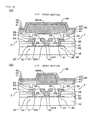
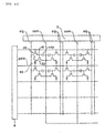
- each pixel region 7 of the display device 1 is described below with reference to Figs. 3 to 6(A).
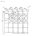
- Fig. 3 is an enlarged plan view illustrating three pixel regions 7 of the plurality of pixels regions 7 formed in the display device 1 according to the present embodiment.
- Figs. 4, 5, and 6(A) are cross-sectional views of Fig. 3, taken along lines A-A', B-B', and C-C', respectively.
- an island-shaped silicon film 200 used to form the first TFT 20 is formed in each pixel region 7 and a gate insulating film 50 is formed on the surface of the silicon film 200, as shown in Fig. 4.
- a gate electrode 21 is formed on the surface of the gate insulating film 50.
- Source/drain regions 22 and 23 are formed by doping a high concentration of impurities in a self-aligned fashion with respect to the gate electrode 21.
- a first insulating film 51 is formed on the upper surface of the gate insulating film 50.
- the source/drain regions 22 and 23 are electrically connected to the data line "sig" and the potential sustaining electrode "st", respectively, via a contact hole 61 or 62 formed in the first insulating film 50.
- a capacitor line “cline” is formed at the same layer where the scanning line “gate” and the gate electrode 21 are formed (that is, at the layer between the gate insulating film 50 and the first interlayer insulating film 51) in each pixel region 7 such that the capacitor line “cline” extends in a direction parallel to the scanning line "gate”.
- An extension “st1" of the potential sustaining electrode “st” is formed such that it overlaps the capacitor line “cline” via the first interlayer insulating film 51.
- a holding capacitor “cap” is formed between the capacitor line “cline” and the extension “st1" of the potential sustaining electrode “st” wherein the first insulating film 51 serves as the dielectric film of the holding capacitor “cap”.
- a second insulating film 52 is formed at a layer above the potential sustaining electrode "st” and the data line "sig”.
- two data lines "sig" used by respective pixel regions 7 are formed close to each other and in parallel to each other, as shown in Fig. 5, at a layer on the first interlayer insulating film 51 formed on the transparent substrate 10 and on the second interlayer insulating film 52.
- an island-shaped silicon film 300 used to form the second TFT 30 is formed, as shown in Fig. 6(A), on the transparent substrate 10 such that the silicon film 300 extends over two pixel regions 7 across a common power supply line "com" located between these two pixel regions 7.
- a gate insulating film 50 is formed on the surface of the silicon film 300.
- Gate electrodes 31 are formed in the respective two pixel regions 7, on the surface of the gate insulating film 50, such that the gate electrodes 31 are located at both sides of the common power supply line "com”.
- Source/drain regions 32 and 33 are formed by doping a high concentration of impurities in a self-aligned fashion with respect to the gate electrodes 31.
- a first interlayer insulating film 51 is formed at a layer on the gate insulating film 50. Interconnecting electrodes 35 are electrically connected to the source/drain regions 32 via contact holes 63 formed in the first interlayer insulating film 51. On the other hand, the part of the silicon film 300 which will be a common source/drain region 33 at the center of two pixel regions 7 is electrically connected to the common power supply line "com" via a contact hole 64 formed in the first interlayer insulating film 51.
- a second interlayer insulating film 52 is formed at a layer over the surface of the common power supply line "com" and also over the surface of the interconnecting electrodes 35. ITO films serving as pixel electrodes 41 are formed on the surface of the second interlayer insulating film 52.
- the pixel electrodes 41 are electrically connected to the respective interconnecting electrodes 35 via contact holes 65 formed in the second interlayer insulating film 52 and further electrically connected to the respective source/drain regions 32 of the second TFTs 30 via the interconnecting electrodes 35.
- Each pixel electrode 41 serves as one of electrodes of a corresponding luminescent element 40. That is, a hole injection layer 42 and an organic semiconductor film 43 are formed in a multilayer fashion on the surface of the pixel electrodes 41, and a metal film of aluminum containing lithium or of calcium serving as an opposite electrode "op" is formed on the surface of the organic semiconductor film 43.
- the opposite electrode "op” is formed at least over the entire areas of all pixel regions 41 or formed in a stripe shape such that it serves as a common electrode maintained at a constant voltage.
- each luminescent element 40 constructed in the above-described fashion, a voltage is applied between the opposite electrode "op" and the pixel electrode 41 serving as positive and negative electrodes, respectively. If the applied voltage becomes greater than a threshold voltage, the current (driving current) flowing through the organic semiconductor film 43 increases abruptly, as shown in Fig. 7. As a result, the luminescent element 40 acts as an electroluminescent element or an LED and emits light. The light emitted from the luminescent element 40 is reflected by the opposite electrode "op” and output to the outside via the transparent pixel electrode 41 and the transparent substrate 10.
- the driving current for emission of light is passed through a current path consisting of the opposite electrode "op", the organic semiconductor film 43, the hole injection layer 42, the pixel electrode 41, the second TFT 30, and the common power supply line "com". Therefore, if the second TFT 30 is turned off, the driving current stops flowing.
- a first TFT 20 is selected and turned on by a scanning signal, an image signal is written into a holding capacitor "cap” from a data line "sig" via the first TFT 20.
- the gate electrode of the second TFT 30 is held by the holding capacitor "cap” at a voltage corresponding to the image signal even after the first TFT 20 is turned off, and thus the second TFT 30 is maintained in the on-state.
- the driving current keeps flowing through the luminescent element 40 and the corresponding pixel keeps emitting light. This state is maintained until the second TFT 30 is turned off after new image data is written into the holding capacitor "cap”.
- the steps from the beginning until the first TFTs 20 and the second TFTs 30 are formed on the transparent substrate 10 are similar to the steps of producing an active matrix substrate for use in a liquid crystal display device 1.
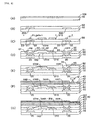
- the outline of the production process is described below with reference to Fig. 8.
- Fig. 8 is a cross-sectional view illustrating the steps of producing various parts of the display device 1.
- a silicon oxide film serving as an underlying protective film (not shown) with a thickness of about 2000 to 5000 A is formed on a transparent substrate 10 by means of a plasma CVD technique using source gases such as TEOS (tetraethoxysilane) and oxygen as required.
- source gases such as TEOS (tetraethoxysilane) and oxygen as required.
- the temperature of the substrate is set to about 350°C, and a semiconductor film 100 of amorphous silicon with a thickness of about 300 to 700 A is formed on the surface of the underlying protective film by means of plasma CVD.
- the semiconductor film 100 of amorphous silicon is then crystallized by means of laser annealing or solid phase growth so as to convert the semiconductor film 100 into a polysilicon film.
- the laser annealing may be performed for example using an excimer laser line beam with a longer side length of 400 mm with an output power of for example 200 mJ/cm 2 .
- the line beams is scanned such that adjacent scanned lines have an overlap at 90% of peak power along the shorter sides of the laser beam.
- the semiconductor film 100 is patterned into islands 200 and 300 of semiconductor film, as shown in Fig. 8(B). Subsequently, a silicon oxide film or a silicon nitride film with a thickness of about 600 to 1500 A serving as a gate insulating film 50 is formed by means of a plasma CVD process using TEOS (tetraethoxysilane) and oxygen as source gases.
- TEOS tetraethoxysilane
- a conductive film is formed by sputtering metal such as aluminum, tantalum, molybdenum, titanium, or tungsten.
- the conductive film is then patterned so as to form gate electrodes 21 and 31 (gate electrode formation step). In this step, scanning lines "gate” and capacitor lines “cline” are also formed.
- reference numeral 310 denotes an extension of the gate electrode 31.
- a first interlayer insulating film 51 is formed and then contact holes 61, 62, 63, 64, and 69 are formed therein. Furthermore, data lines "sig”, capacitor lines “cline”, potential sustaining electrodes “st” including extensions “st1” overlapping extensions 310 of the gate electrodes 31, common power supply lines “com”, and interconnecting electrodes 35 are formed. As a result, the potential sustaining electrodes "st” are electrically connected to the corresponding gate electrodes 31 via corresponding contact holes 69 and extensions 310. Thus, the first TFTs 20 and the second TFTs 30 are obtained. Furthermore, the holding capacitors "cap” are formed between the respective capacitor lines “cline” and the extensions "st1" of the potential sustaining electrodes "st”.
- a second insulating film 52 is formed and then contact holes 65 are formed in this second insulating film 52, at locations corresponding to the interconnecting electrodes 35.
- an ITO film is formed over the entire surface of the second insulating film 52. The ITO film is then patterned so as to form pixel electrodes electrically connected to source/drain regions 32 of the corresponding second TFTs 30 via contact holes 65.
- a black resist layer is formed on the surface of the second interlayer insulating film 52.
- the resist layer is then patterned into the shape of the bank layer "bank” surrounding the light emitting areas where the hole injection layers 42 and the organic semiconductor films 43 of the respective luminescent elements 40 will be formed.
- the organic semiconductor films 43 may be formed in the form of, for example, isolated boxes in the respective pixels or in the form of stripes extending along the data lines "sig". In any case, it is simply required to form the bank layer "bank” into the corresponding shape according to the production method of the present embodiment.
- a liquid material (precursor) for forming the hole injection layers 42 is emitted from an ink-jet head IJ into the inner areas surrounded by the bank layer "bank” thereby forming the hole injection layers 42 in the inner areas surrounded by the bank layer "bank”.
- a liquid material (precursor) for forming the organic semiconductor films 43 is emitted from the ink-jet head IJ into the inner areas surrounded by the bank layer "bank” thereby forming the organic semiconductor films 43 in the inner areas surrounded by the bank layer "bank”. Because the bank layer is formed of the resist, the bank layer is water repellent.
- the precursor of the organic semiconductor films 43 is in the form of a hydrophilic solvent.
- the bank layer "bank” is formed to have partition walls as high as about 1 ⁇ m, the partitions walls of the back layer “bank” can work well even if the bank layer "bank” is not water repellent.
- the bank layer "bank” may also be used to define the areas where the hole injection layers 42 and the organic semiconductor films 43 are formed by means of a coating technique instead of the ink-jet technique.
- the center-to-center pitch P of the areas where the organic semiconductor film 43 is formed is set to an equal value over the all pixel areas 7 arranged in the direction along the scanning lines "gate" as shown in Fig. 3 thereby achieving high productivity.
- high productivity can be achieved. Because the requirement for the ink-jet head IJ is only to move at equal intervals, high emission accuracy can be achieved using a simple mechanism for moving the ink-jet head IJ.
- the opposite electrode "op" is formed on the entire area of the surface of the transparent substrate 10 or into the shape of stripes.
- the bank layer "bank” made of the black resist is left in place so that it serves as a black matrix BM and also as an insulating layer for reducing the parasitic capacitance.
- TFTs are also formed in the data line driving circuit 3 and the scanning line driving circuit 4 shown in Fig. 1 wherein these TFTs may be formed using all or part of the above-described processing steps used to form the TFTs in the pixel areas. Therefore, the TFTs in the driving circuits are formed at the same layer where the TFTs in the pixel regions 7 are formed.
- Both the first TFTs 20 and the second TFTs 30 may be of either the N-type or P-type. Otherwise, either the first TFTs 20 or the second TFTs 30 may be of the N-type and the other may be of the P-type. In any case, the TFTs may be produced using a known technique and thus the production method of the TFTs is not described in further detail herein.
- the hole injection layer 42 may be removed although the luminous efficiency slightly decreases.
- an electron injection layer is formed instead of the hole injection layer 42 on the organic semiconductor film 43 on the side opposite to the hole injection layer 42, both the hole injection layer 42 and the electron injection layer may be formed.
- the above-described bank layer "bank” is formed over the entire peripheral area (diagonally shaded area in Fig. 1) on the transparent substrate 10 shown in Fig. 1.
- the data driving circuit 3 and the scanning line driving circuit 4 are covered with the bank layer "bank”. Therefore, when the opposite electrode "op" is formed such that it extends over the area where the driving circuits are formed, the bank layer "bank” is present between the opposite electrode “op” and the interconnection layers in the driving circuits.
- the driving circuits 3 and 4 are prevented from having parasitic capacitance. This result in a reduction in the load of the driving circuits 3 and 4, and thus a reduction in power consumption and an increase in the speed of displaying operation are achieved.
- the bank layer "bank” is formed such that it extends over the data lines "sig” and thus the bank layer “bank” is also present between the opposite electrode “op” and the data lines "sig".
- the data lines "sig” are prevented from having parasitic capacitance. This results in a reduction in the load of the data line driving circuit 3. Therefore, it is possible to achieve a reduction in power consumption and an increase in the speed of displaying operation.
- the bank layer "bank” is also formed such that the area of each pixel electrode 41 overlapping the interconnecting electrode 31 is covered with the bank layer "bank". If there were no bank layer "bank” in this area overlapping the interconnecting electrode 35 as shown in Fig. 6(B), a driving current would flow in this area between the opposite electrode "op” and the pixel electrode 41 and the organic semiconductor film 43 in this area would emit light. However, the light emitted from such an area would be confined between the interconnecting electrode 35 and the opposite electrode "op” and it would not be emitted to the outside. As a result, the light would not make any contribution to displaying of an image. Thus, such a driving current is useless.
- the bank layer "bank” is formed in the area where a useless current would otherwise flow so that the driving current is prevented from flowing in this area. This also prevents the useless current from flowing through the common power supply lines "com”. Therefore, it is possible to reduce the width of the common power supply line "com” by an amount corresponding to the reduction in the current.
- the power supply lines "com” unlike the data lines "sig", are required to carry a large current for driving the luminescent elements 40. That is, each common power supply line "com” is required to supply a driving current to two lines of pixels.
- the common power supply lines “com” are formed using the same material as that of the data lines “sig” but they have a width greater than the width of the data lines “sig” so that the resistance of the common power supply lines “com” per unit length becomes lower than the resistance of the data lines “sig” per unit length.
- the width of the common power supply lines “com” may be reduced to a minimum required level. This allows the light emitting area of the pixel regions 7 to be increased. Thus, the display performance such as the brightness and the contrast can be improved.
- the bank layer “bank” may serve as a black matrix which results in an improvement in the display performance such as the contrast.
- the opposite electrode “op” is formed on the transparent substrate 10 over the entire pixel regions 7 or into the shape of stripes over a wide area, light reflected by the opposite electrode “op” can degrade the contrast.
- the bank layer is formed of the black resist so that it serves as the black matrix which blocks light reflected from the opposite electrode "op” and thus the contrast is improved, wherein the bank layer also serves to prevent the parasitic capacitance.
- one common power supply line “com” is formed for every two lines of pixel regions 7 such that the common power supply line “com” is located at the center of the two lines of pixel regions and such that pixel regions 7 at both sides of the common power supply line “com” are supplied with the driving current via that common power supply line “com”.
- two data lines “sig” are formed at locations which are close to each other such that they extend over the pixel areas 7 on the side opposite to the common power supply line "com”. In this structure, crosstalk can occur between the two data lines "sig".
- a dummy interconnection layer DA is formed between the two data lines "sig” as shown in Fig. 9 and Figs.
- the dummy interconnection layer DA may be realized using, for example, an ITO film DA1 formed at the same time as the pixel electrodes 41.
- the dummy interconnection layer DA may be realized using an extension DA2 formed by extending the capacitor line "cline” into the area between the two data line "sig". Furthermore, both may be employed as the dummy interconnection layer DA.
- the crosstalk can be prevented simply by maintaining the interconnection layer DA (DA1, DA2) at a constant voltage at least for one horizontal scanning period.
- the first interlayer insulating film 51 and the second interlayer insulating film 52 have a thickness of about 1.0 ⁇ m
- the spacing between the two data lines "sig” is about 2 ⁇ m or greater. Therefore, the capacitance between the two data lines "sig” is negligibly small compared to the capacitance between the dummy interconnection layer DA (DA1, DA2) and either data line "sig".
- DA1, DA2 the capacitance between the two data lines "sig” is negligibly small compared to the capacitance between the dummy interconnection layer DA (DA1, DA2) and either data line "sig".
- the holding capacitors "cap” are formed using the capacitor lines “cline” (capacitor electrodes), the holding capacitors “cap” may also be formed using the polysilicon film used to form the TFTs as described earlier with reference to the conventional technique.
- the holding capacitors "cap” may also be formed between the common power supply lines “com” and the potential sustaining electrodes “st” as shown in Fig. 11.
- the extension 310 of each gate electrode 31 for electrically connecting the gate electrode 31 to the corresponding potential sustaining electrode “st” is extended to a location under the corresponding common power supply line “com” so that the holding capacitor “cap” is formed between the extension 310 and the common power supply line "com” wherein the first interlayer insulating film 51 serves as the dielectric film of the holding capacitor "cap”.
- the display device is characterized in that the insulating bank layer for defining the areas where the organic semiconductor films of the luminescent elements are formed is also formed between the opposite electrode and the data lines or between the opposite electrode and the driving circuits.
- the insulating bank layer for defining the areas where the organic semiconductor films of the luminescent elements are formed is also formed between the opposite electrode and the data lines or between the opposite electrode and the driving circuits.
Description
- 1
- Display device;
- 2
- Display area;
- 3
- Data line driving circuit (First driving circuit);
- 4
- Scanning line driving circuit (Second driving circuit);
- 5
- Test circuit;
- 6
- Mounting pad;
- 7
- Pixel region;
- 10
- Transparent substrate;
- 20
- First TFT;
- 21
- Gate electrode of the first TFT;
- 30
- Second TFT;
- 31
- Gate electrode of the second TFT;
- 40
- Luminescent element;
- 41
- Pixel electrode;
- 42
- Hole injection layer;
- 43
- Organic semiconductor film;
- 50
- Gate insulating film;
- 51
- First interlayer insulating film;
- 52
- Second interlayer insulating film;
- DA
- Dummy interconnection layer;
- bank
- Bank layer;
- cap
- Holding capacitor;
- cline
- Capacitor line;
- com
- Common power supply line;
- gate
- Scanning line;
- op
- Opposite electrode;
- sig
- Data line; and
- st
- Potential sustaining electrode.
Claims (12)
- A display device (1) comprising elements formed on a substrate (10), said elements including: a plurality of scanning lines (gate); a plurality of data lines (sig) extending in a direction crossing the direction in which said scanning lines (gate) extend; a plurality of common power supply lines (com) extending in a direction parallel to said data lines (sig); and pixel regions (7) formed in the shape of a matrix defined by said data lines (sig) and said scanning lines (gate), each said pixel region (7) including: a first thin film transistor (20) having a gate electrode (21) to which a scanning signal is supplied via one of the scanning lines (gate); a holding capacitor (cap) for holding an image signal supplied from a corresponding data line via said first thin film transistor (20); a second thin film transistor (30) having a gate electrode (31) to which said image signal held by said holding capacitor (cap) is supplied; and a luminescent element (40) including an organic semiconductor film (43) formed between a pixel electrode (41) provided in each pixel region (7) and an opposite electrode (op) extending across the data lines (sig) such that said opposite electrode (op) faces the plurality of pixel electrodes (41), said luminescent element (40) being adapted to emit light when said organic semiconductor film(43) is driven by a driving current which flows between said pixel electrode (41) and said opposite electrode (op) when said pixel electrode (41) is electrically connected to a corresponding common power supply line (com) via said second thin film transistor (30); and
characterised in that light emitting areas of said organic semiconductor film (43) are surrounded by a bank layer(bank) made up of an insulating film having a thickness greater than that of said organic semiconductor film (43), said bank layer (bank) being formed such that said data lines (sig) are, at least partly, covered with said bank layer (bank). - A display device (1) according to Claim 1, wherein on said substrate (10), there is also formed, together with said plurality of pixel regions (7), at least either one of or both of a first driving circuit (3) for outputting said image signal over said data lines (sig) and a second driving circuit (4) for outputting said scanning signal over said scanning lines (gate), and wherein said at least either one of or both of driving circuits (3, 4) are covered with said bank layer (bank).
- A display device (1) comprising elements formed on a substrate (10), said elements including: a plurality of scanning lines (gate); a plurality of data lines (sig) extending in a direction perpendicular to the direction in which said scanning lines (gate) extend; a plurality of common power supply lines (com) extending in a direction parallel to said data lines (sig); at least one of or both of a first driving circuit (3) for outputting an image signal over said data lines (sig) and a second driving circuit (4) for outputting a scanning signal over said scanning lines (gate); and pixel regions (7) formed in the shape of a matrix defined by said data lines (sig) and said scanning lines (gate), each said pixel region including: a first thin film transistor (20) having a gate electrode (21) to which the scanning signal is supplied via one of the scanning lines (gate); a holding capacitor (cap) for holding the image signal supplied from a corresponding data line (sig) via said first thin film transistor (20); a second thin film transistor (30) having a gate electrode (31) to which said image signal held by said holding capacitor (cap) is supplied; and a luminescent element (40) including an organic semiconductor film (43) formed between a pixel electrode (41) provided in each pixel region (7) and an opposite electrode (op) extending across the data lines (sig) such that said opposite electrode (op) faces the plurality of pixel electrodes (41), said luminescent element (40) being adapted to emit light when said organic semiconductor film (43) is driven by a driving current which flows between said pixel electrode (41) and said opposite electrode (op) when said pixel electrode (41) is electrically connected to a corresponding common power supply line (com) via said second thin film transistor (30); and
characterised in that light emitting areas of said organic semiconductor film (43) are surrounded by a bank layer (bank) made up of an insulating film having a thickness greater than that of said organic semiconductor film (43), said bank layer (bank) being formed such that said at least one of or both of driving circuits (34) are covered with said bank layer (bank). - A display device (1) according to any of Claims 1 to 3, wherein said organic semiconductor film (43) is a film formed by means of an ink-jet technique in the areas surrounded by said bank layer (bank), and wherein said bank layer (bank) is a water repellent film.
- A display device (1) according to any of Claims 1 to 3, wherein said organic semiconductor film (43) is a film formed by means of an ink-jet technique in the areas surrounded by said bank layer (bank), and wherein said bank layer (bank) has a thickness equal to or greater than 1 µm.
- A display device (1) according to any of Claims 1 to 5, wherein an area of each said pixel electrode (41) overlapping the corresponding first thin film transistor (20) or second thin film transistor (30) is covered with said bank layer (bank).
- A display device ( 1) according to any of Claims 1 to 6, wherein said bank layer (bank) is formed of a black resist film.
- A display device (1) according to any of Claims 1 to 7, wherein the resistance of said common power supply lines (com) per unit length is smaller than the resistance of said data lines (sig) per unit length.
- A display device (1) according to any of Claims 1 to 7, wherein said common power supply lines (com) and said data lines (sig) are made of the same material and have the same thickness whereas the width of said common power supply lines (com) is greater than the width of said data lines (sig).
- A display device (1) according to any of Claims I to 9, wherein pixel regions (7) located at both sides of each said common power supply line (com) are supplied with said driving current via this common power supply line (com), and data lines (sig) extend over said pixel regions (7) on the respective sides opposite to said common power supply line (com).
- A display device (1) according to Claim 10, wherein an interconnection layer is formed between the two data lines (sig) extending, across said pixel regions (7), on the sides opposite to each said common power supply line (com).
- A display device (1) according to any of Claims 1 to 11, wherein the center-to-center pitch of the organic semiconductor film (43) areas is equal in all pixel regions (7) located along a direction parallel to the direction in which said scanning lines (gate) extend.
Priority Applications (1)
| Application Number | Priority Date | Filing Date | Title |
|---|---|---|---|
| EP04078121A EP1505649A3 (en) | 1997-07-02 | 1998-07-01 | Display device |
Applications Claiming Priority (3)
| Application Number | Priority Date | Filing Date | Title |
|---|---|---|---|
| JP17745497A JP3541625B2 (en) | 1997-07-02 | 1997-07-02 | Display device and active matrix substrate |
| JP17745497 | 1997-07-02 | ||
| PCT/JP1998/002983 WO1999001857A1 (en) | 1997-07-02 | 1998-07-01 | Display |
Related Child Applications (1)
| Application Number | Title | Priority Date | Filing Date |
|---|---|---|---|
| EP04078121A Division EP1505649A3 (en) | 1997-07-02 | 1998-07-01 | Display device |
Publications (3)
| Publication Number | Publication Date |
|---|---|
| EP0932137A1 EP0932137A1 (en) | 1999-07-28 |
| EP0932137A4 EP0932137A4 (en) | 2002-08-21 |
| EP0932137B1 true EP0932137B1 (en) | 2005-03-16 |
Family
ID=16031236
Family Applications (2)
| Application Number | Title | Priority Date | Filing Date |
|---|---|---|---|
| EP98929803A Expired - Lifetime EP0932137B1 (en) | 1997-07-02 | 1998-07-01 | Display |
| EP04078121A Withdrawn EP1505649A3 (en) | 1997-07-02 | 1998-07-01 | Display device |
Family Applications After (1)
| Application Number | Title | Priority Date | Filing Date |
|---|---|---|---|
| EP04078121A Withdrawn EP1505649A3 (en) | 1997-07-02 | 1998-07-01 | Display device |
Country Status (8)
| Country | Link |
|---|---|
| US (2) | US6194837B1 (en) |
| EP (2) | EP0932137B1 (en) |
| JP (1) | JP3541625B2 (en) |
| KR (2) | KR100526930B1 (en) |
| CN (1) | CN1169099C (en) |
| DE (1) | DE69829353T2 (en) |
| TW (1) | TW388853B (en) |
| WO (1) | WO1999001857A1 (en) |
Cited By (5)
| Publication number | Priority date | Publication date | Assignee | Title |
|---|---|---|---|---|
| US8405594B2 (en) | 1999-06-21 | 2013-03-26 | Semiconductor Energy Laboratory Co., Ltd. | EL display device, driving method thereof, and electronic equipment provided with the EL display device |
| US9087476B2 (en) | 2000-01-17 | 2015-07-21 | Semiconductor Energy Laboratory Co., Ltd. | Display system and electrical appliance |
| US9263469B2 (en) | 2000-02-01 | 2016-02-16 | Semiconductor Energy Laboratory Co., Ltd. | Semiconductor device and manufacturing method thereof |
| US9419026B2 (en) | 2000-04-27 | 2016-08-16 | Semiconductor Energy Laboratory Co., Ltd. | Semiconductor device and method of fabricating the same |
| US9431431B2 (en) | 1999-02-23 | 2016-08-30 | Semiconductor Energy Laboratory Co., Ltd. | Semiconductor device and fabrication method thereof |
Families Citing this family (214)
| Publication number | Priority date | Publication date | Assignee | Title |
|---|---|---|---|---|
| US4736683A (en) * | 1986-08-05 | 1988-04-12 | Exxon Chemical Patents Inc. | Dry ammonium nitrate blasting agents |
| JP3541625B2 (en) * | 1997-07-02 | 2004-07-14 | セイコーエプソン株式会社 | Display device and active matrix substrate |
| JP3520396B2 (en) | 1997-07-02 | 2004-04-19 | セイコーエプソン株式会社 | Active matrix substrate and display device |
| WO1999010862A1 (en) | 1997-08-21 | 1999-03-04 | Seiko Epson Corporation | Active matrix display |
| JP3729195B2 (en) * | 1997-08-21 | 2005-12-21 | セイコーエプソン株式会社 | Organic electroluminescence device and manufacturing method thereof |
| JP3803355B2 (en) * | 1997-08-21 | 2006-08-02 | セイコーエプソン株式会社 | Method for manufacturing organic electroluminescence device |
| JP3580092B2 (en) * | 1997-08-21 | 2004-10-20 | セイコーエプソン株式会社 | Active matrix display |
| JP3729196B2 (en) * | 1997-08-21 | 2005-12-21 | セイコーエプソン株式会社 | Organic electroluminescence device |
| JP3803342B2 (en) * | 1997-08-21 | 2006-08-02 | セイコーエプソン株式会社 | Method for forming organic semiconductor film and method for manufacturing active matrix substrate |
| JP3690406B2 (en) * | 1997-08-21 | 2005-08-31 | セイコーエプソン株式会社 | Organic electroluminescence device |
| JP3830238B2 (en) * | 1997-08-29 | 2006-10-04 | セイコーエプソン株式会社 | Active matrix type device |
| JP3838669B2 (en) * | 1997-10-20 | 2006-10-25 | シチズン時計株式会社 | Integrated circuit for liquid crystal drive |
| JP2000163014A (en) * | 1998-11-27 | 2000-06-16 | Sanyo Electric Co Ltd | Electroluminescence display device |
| JP3850005B2 (en) * | 1999-03-03 | 2006-11-29 | パイオニア株式会社 | Switching element and organic electroluminescence element display device |
| TW444257B (en) * | 1999-04-12 | 2001-07-01 | Semiconductor Energy Lab | Semiconductor device and method for fabricating the same |
| US6512504B1 (en) * | 1999-04-27 | 2003-01-28 | Semiconductor Energy Laborayory Co., Ltd. | Electronic device and electronic apparatus |
| JP4298131B2 (en) * | 1999-05-14 | 2009-07-15 | 株式会社半導体エネルギー研究所 | Method for manufacturing liquid crystal display device |
| KR100316271B1 (en) * | 1999-05-27 | 2001-12-12 | 구본준, 론 위라하디락사 | An eld and fabricating method thereof |
| EP1058310A3 (en) * | 1999-06-02 | 2009-11-18 | Sel Semiconductor Energy Laboratory Co., Ltd. | Semiconductor device and manufacturing method thereof |
| US7288420B1 (en) * | 1999-06-04 | 2007-10-30 | Semiconductor Energy Laboratory Co., Ltd. | Method for manufacturing an electro-optical device |
| US8853696B1 (en) * | 1999-06-04 | 2014-10-07 | Semiconductor Energy Laboratory Co., Ltd. | Electro-optical device and electronic device |
| JP4265818B2 (en) * | 1999-06-04 | 2009-05-20 | 株式会社半導体エネルギー研究所 | Electro-optic device |
| TW527735B (en) * | 1999-06-04 | 2003-04-11 | Semiconductor Energy Lab | Electro-optical device |
| JP4627822B2 (en) | 1999-06-23 | 2011-02-09 | 株式会社半導体エネルギー研究所 | Display device |
| TW556357B (en) | 1999-06-28 | 2003-10-01 | Semiconductor Energy Lab | Method of manufacturing an electro-optical device |
| JP4472073B2 (en) * | 1999-09-03 | 2010-06-02 | 株式会社半導体エネルギー研究所 | Display device and manufacturing method thereof |
| JP2001100656A (en) | 1999-09-29 | 2001-04-13 | Sanyo Electric Co Ltd | Active matrix type el display device |
| JP2001109404A (en) * | 1999-10-01 | 2001-04-20 | Sanyo Electric Co Ltd | El display device |
| TW480722B (en) | 1999-10-12 | 2002-03-21 | Semiconductor Energy Lab | Manufacturing method of electro-optical device |
| TW535454B (en) * | 1999-10-21 | 2003-06-01 | Semiconductor Energy Lab | Electro-optical device |
| US6587086B1 (en) | 1999-10-26 | 2003-07-01 | Semiconductor Energy Laboratory Co., Ltd. | Electro-optical device |
| US6384427B1 (en) * | 1999-10-29 | 2002-05-07 | Semiconductor Energy Laboratory Co., Ltd. | Electronic device |
| US6580094B1 (en) * | 1999-10-29 | 2003-06-17 | Semiconductor Energy Laboratory Co., Ltd. | Electro luminescence display device |
| TW484117B (en) * | 1999-11-08 | 2002-04-21 | Semiconductor Energy Lab | Electronic device |
| JP2001148291A (en) * | 1999-11-19 | 2001-05-29 | Sony Corp | Display device and its manufacturing method |
| JP4727029B2 (en) * | 1999-11-29 | 2011-07-20 | 株式会社半導体エネルギー研究所 | EL display device, electric appliance, and semiconductor element substrate for EL display device |
| CN1293642C (en) * | 1999-11-29 | 2007-01-03 | 皇家菲利浦电子有限公司 | Organic electroluminescent device and method of manufacturing thereof |
| JP4906145B2 (en) * | 1999-11-29 | 2012-03-28 | 株式会社半導体エネルギー研究所 | EL display device |
| JP4759719B2 (en) * | 2000-02-01 | 2011-08-31 | モトローラ ソリューションズ インコーポレイテッド | Light emitting device and manufacturing method |
| EP1122793A2 (en) * | 2000-02-01 | 2001-08-08 | Canon Kabushiki Kaisha | Production of organic luminescence device |
| TW521303B (en) * | 2000-02-28 | 2003-02-21 | Semiconductor Energy Lab | Electronic device |
| TW507258B (en) | 2000-02-29 | 2002-10-21 | Semiconductor Systems Corp | Display device and method for fabricating the same |
| TW495812B (en) | 2000-03-06 | 2002-07-21 | Semiconductor Energy Lab | Thin film forming device, method of forming a thin film, and self-light-emitting device |
| JP2001267578A (en) * | 2000-03-17 | 2001-09-28 | Sony Corp | Thin-film semiconductor device, and method for manufacturing the same |
| TW521226B (en) * | 2000-03-27 | 2003-02-21 | Semiconductor Energy Lab | Electro-optical device |
| TW493282B (en) * | 2000-04-17 | 2002-07-01 | Semiconductor Energy Lab | Self-luminous device and electric machine using the same |
| JP4889872B2 (en) * | 2000-04-17 | 2012-03-07 | 株式会社半導体エネルギー研究所 | Light emitting device and electric appliance using the same |
| KR100649722B1 (en) * | 2000-04-21 | 2006-11-24 | 엘지.필립스 엘시디 주식회사 | Apparatus for Patterning Electro-luminescence Display Device and Method of Patterning Electro-luminescence Display Device using the same |
| US7579203B2 (en) | 2000-04-25 | 2009-08-25 | Semiconductor Energy Laboratory Co., Ltd. | Light emitting device |
| JP2002014628A (en) * | 2000-04-27 | 2002-01-18 | Semiconductor Energy Lab Co Ltd | Semiconductor device and its manufacturing method |
| US7633471B2 (en) | 2000-05-12 | 2009-12-15 | Semiconductor Energy Laboratory Co., Ltd. | Light-emitting device and electric appliance |
| TW554638B (en) * | 2000-05-12 | 2003-09-21 | Semiconductor Energy Lab | Light emitting device |
| US8610645B2 (en) | 2000-05-12 | 2013-12-17 | Semiconductor Energy Laboratory Co., Ltd. | Display device |
| US6762735B2 (en) * | 2000-05-12 | 2004-07-13 | Semiconductor Energy Laboratory Co., Ltd. | Electro luminescence display device and method of testing the same |
| US7339317B2 (en) * | 2000-06-05 | 2008-03-04 | Semiconductor Energy Laboratory Co., Ltd. | Light-emitting device having triplet and singlet compound in light-emitting layers |
| GB0014962D0 (en) * | 2000-06-20 | 2000-08-09 | Koninkl Philips Electronics Nv | Matrix array display devices with light sensing elements and associated storage capacitors |
| TW466466B (en) * | 2000-06-21 | 2001-12-01 | Chi Mei Optoelectronics Corp | Driving circuit of thin film transistor light emitting display and the usage method thereof |
| JP3815269B2 (en) * | 2000-07-07 | 2006-08-30 | セイコーエプソン株式会社 | Organic EL display and manufacturing method thereof, perforated substrate, electro-optical device and manufacturing method thereof, and electronic apparatus |
| US7019718B2 (en) | 2000-07-25 | 2006-03-28 | Semiconductor Energy Laboratory Co., Ltd. | Display device |
| KR100344810B1 (en) * | 2000-07-26 | 2002-07-20 | 엘지전자주식회사 | current drive circuit using high voltage element |
| US6864628B2 (en) * | 2000-08-28 | 2005-03-08 | Semiconductor Energy Laboratory Co., Ltd. | Light emitting device comprising light-emitting layer having triplet compound and light-emitting layer having singlet compound |
| JP2002083691A (en) * | 2000-09-06 | 2002-03-22 | Sharp Corp | Active matrix driven organic led display unit and its manufacturing method |
| US6739931B2 (en) * | 2000-09-18 | 2004-05-25 | Semiconductor Energy Laboratory Co., Ltd. | Display device and method of fabricating the display device |
| US6924594B2 (en) * | 2000-10-03 | 2005-08-02 | Semiconductor Energy Laboratory Co., Ltd. | Light emitting device |
| JP4127608B2 (en) * | 2000-10-20 | 2008-07-30 | 東芝松下ディスプレイテクノロジー株式会社 | Self-luminous display panel |
| TW522752B (en) | 2000-10-20 | 2003-03-01 | Toshiba Corp | Self-luminous display panel and method of manufacturing the same |
| US7009203B2 (en) | 2000-12-14 | 2006-03-07 | Samsung Soi Co., Ltd. | Organic EL device and method for manufacturing the same |
| KR100365519B1 (en) * | 2000-12-14 | 2002-12-18 | 삼성에스디아이 주식회사 | Electroluminescence device and method for fabricating thereof |
| JP2002208484A (en) * | 2001-01-12 | 2002-07-26 | Tohoku Pioneer Corp | Organic el display, and manufacturing method of the same |
| JP4011292B2 (en) * | 2001-01-15 | 2007-11-21 | 株式会社日立製作所 | LIGHT EMITTING ELEMENT AND DISPLAY DEVICE |
| TW525402B (en) | 2001-01-18 | 2003-03-21 | Semiconductor Energy Lab | Process for producing a light emitting device |
| SG118110A1 (en) | 2001-02-01 | 2006-01-27 | Semiconductor Energy Lab | Organic light emitting element and display device using the element |
| JP3797877B2 (en) * | 2001-02-05 | 2006-07-19 | シャープ株式会社 | Active matrix drive organic LED display |
| SG143945A1 (en) | 2001-02-19 | 2008-07-29 | Semiconductor Energy Lab | Light emitting device and method of manufacturing the same |
| US6720198B2 (en) * | 2001-02-19 | 2004-04-13 | Semiconductor Energy Laboratory Co., Ltd. | Light emitting device and manufacturing method thereof |
| US7301279B2 (en) * | 2001-03-19 | 2007-11-27 | Semiconductor Energy Laboratory Co., Ltd. | Light-emitting apparatus and method of manufacturing the same |
| JP2002289357A (en) * | 2001-03-28 | 2002-10-04 | Pioneer Electronic Corp | Organic electroluminescence display panel |
| JP2003017264A (en) * | 2001-04-27 | 2003-01-17 | Canon Inc | Electroluminescent element and image display device |
| JP4831885B2 (en) | 2001-04-27 | 2011-12-07 | 株式会社半導体エネルギー研究所 | Method for manufacturing semiconductor device |
| TW588570B (en) * | 2001-06-18 | 2004-05-21 | Semiconductor Energy Lab | Light emitting device and method of fabricating the same |
| JP4982014B2 (en) * | 2001-06-21 | 2012-07-25 | 株式会社日立製作所 | Image display device |
| KR20040029385A (en) * | 2001-08-01 | 2004-04-06 | 남 영 김 | Display system |
| US7209101B2 (en) * | 2001-08-29 | 2007-04-24 | Nec Corporation | Current load device and method for driving the same |
| JP4380954B2 (en) * | 2001-09-28 | 2009-12-09 | 三洋電機株式会社 | Active matrix display device |
| JP3899886B2 (en) * | 2001-10-10 | 2007-03-28 | 株式会社日立製作所 | Image display device |
| DE10152919A1 (en) * | 2001-10-26 | 2003-05-22 | Osram Opto Semiconductors Gmbh | Organic electroluminescent display |
| JP4103373B2 (en) * | 2001-11-08 | 2008-06-18 | 松下電器産業株式会社 | Electroluminescence display device and method of manufacturing electroluminescence display device |
| US7042024B2 (en) | 2001-11-09 | 2006-05-09 | Semiconductor Energy Laboratory Co., Ltd. | Light emitting apparatus and method for manufacturing the same |
| JP4149168B2 (en) | 2001-11-09 | 2008-09-10 | 株式会社半導体エネルギー研究所 | Light emitting device |
| KR100814339B1 (en) * | 2001-11-16 | 2008-03-18 | 엘지.필립스 엘시디 주식회사 | Reflective Liquid Crystal Display Device having a Cholesteric Liquid Crystal Color Filter |
| US7483001B2 (en) * | 2001-11-21 | 2009-01-27 | Seiko Epson Corporation | Active matrix substrate, electro-optical device, and electronic device |
| JP3983037B2 (en) | 2001-11-22 | 2007-09-26 | 株式会社半導体エネルギー研究所 | Light emitting device and manufacturing method thereof |
| JP2003159786A (en) * | 2001-11-28 | 2003-06-03 | Seiko Epson Corp | Ejection method and its apparatus, electro-optic device, method and apparatus for manufacturing the device, color filter, method and apparatus for manufacturing the filter, device with substrate, and method and apparatus for manufacturing the device |
| US6949883B2 (en) | 2001-12-06 | 2005-09-27 | Seiko Epson Corporation | Electro-optical device and an electronic apparatus |
| CN1245703C (en) * | 2001-12-11 | 2006-03-15 | 精工爱普生株式会社 | Display device and electronic machine |
| CN1209662C (en) * | 2001-12-17 | 2005-07-06 | 精工爱普生株式会社 | Display device and electronic apparatus |
| JP4265210B2 (en) * | 2001-12-17 | 2009-05-20 | セイコーエプソン株式会社 | Organic EL device and electronic device |
| JP2003186420A (en) * | 2001-12-21 | 2003-07-04 | Seiko Epson Corp | Active matrix substrate, electrooptic device, manufacturing method for electrooptic device, and electronic equipment |
| KR100453634B1 (en) * | 2001-12-29 | 2004-10-20 | 엘지.필립스 엘시디 주식회사 | an active matrix organic electroluminescence display |
| US7109653B2 (en) * | 2002-01-15 | 2006-09-19 | Seiko Epson Corporation | Sealing structure with barrier membrane for electronic element, display device, electronic apparatus, and fabrication method for electronic element |
| US7038377B2 (en) * | 2002-01-16 | 2006-05-02 | Seiko Epson Corporation | Display device with a narrow frame |
| JP3818261B2 (en) * | 2002-01-24 | 2006-09-06 | セイコーエプソン株式会社 | LIGHT EMITTING DEVICE AND ELECTRONIC DEVICE |
| KR100845557B1 (en) * | 2002-02-20 | 2008-07-10 | 삼성전자주식회사 | Active matrix organic light emitting device and method of manufacturing the same |
| JP2003330387A (en) * | 2002-03-05 | 2003-11-19 | Sanyo Electric Co Ltd | Display apparatus |
| JP3783637B2 (en) | 2002-03-08 | 2006-06-07 | セイコーエプソン株式会社 | Material removal method, substrate recycling method, display device manufacturing method, and electronic apparatus including a display device manufactured by the manufacturing method |
| KR100461467B1 (en) * | 2002-03-13 | 2004-12-13 | 엘지.필립스 엘시디 주식회사 | an active matrix organic electroluminescence display device |
| JP4015044B2 (en) * | 2002-03-20 | 2007-11-28 | セイコーエプソン株式会社 | WIRING BOARD, ELECTRONIC DEVICE, AND ELECTRONIC DEVICE |
| US7148508B2 (en) | 2002-03-20 | 2006-12-12 | Seiko Epson Corporation | Wiring substrate, electronic device, electro-optical device, and electronic apparatus |
| GB0216053D0 (en) * | 2002-03-20 | 2002-08-21 | Koninkl Philips Electronics Nv | Active matrix electroluminescent display devices and their manufacture |
| GB0216055D0 (en) | 2002-03-20 | 2002-08-21 | Koninkl Philips Electronics Nv | Active matrix electroluminescent display devices and their manufacture |
| US7106282B2 (en) * | 2002-03-22 | 2006-09-12 | Dai Nippon Printing Co., Ltd. | Image display |
| KR101037118B1 (en) * | 2002-04-03 | 2011-05-26 | 가부시키가이샤 한도오따이 에네루기 켄큐쇼 | Light emitting device |
| KR100461634B1 (en) * | 2002-04-15 | 2004-12-14 | 엘지.필립스 엘시디 주식회사 | The organic electro-luminescence device and method for fabricating of the same |
| JP3787839B2 (en) * | 2002-04-22 | 2006-06-21 | セイコーエプソン株式会社 | Device manufacturing method, device and electronic apparatus |
| JP3965562B2 (en) * | 2002-04-22 | 2007-08-29 | セイコーエプソン株式会社 | Device manufacturing method, device, electro-optical device, and electronic apparatus |
| US7579771B2 (en) | 2002-04-23 | 2009-08-25 | Semiconductor Energy Laboratory Co., Ltd. | Light emitting device and method of manufacturing the same |
| US7786496B2 (en) | 2002-04-24 | 2010-08-31 | Semiconductor Energy Laboratory Co., Ltd. | Semiconductor device and method of manufacturing same |
| JP2003317971A (en) | 2002-04-26 | 2003-11-07 | Semiconductor Energy Lab Co Ltd | Light emitting device and its producing method |
| JP3986051B2 (en) * | 2002-04-30 | 2007-10-03 | 株式会社半導体エネルギー研究所 | Light emitting device, electronic equipment |
| US7242140B2 (en) * | 2002-05-10 | 2007-07-10 | Seiko Epson Corporation | Light emitting apparatus including resin banks and electronic device having same |
| US7897979B2 (en) | 2002-06-07 | 2011-03-01 | Semiconductor Energy Laboratory Co., Ltd. | Light emitting device and manufacturing method thereof |
| US6738113B2 (en) * | 2002-06-10 | 2004-05-18 | Allied Material Corp. | Structure of organic light-emitting material TFT LCD and the method for making the same |
| US6734930B2 (en) * | 2002-06-10 | 2004-05-11 | Allied Material Corp. | Structure of organic light-emitting TFT LCD and method of making the same |
| JP4216008B2 (en) * | 2002-06-27 | 2009-01-28 | 株式会社半導体エネルギー研究所 | LIGHT EMITTING DEVICE AND ITS MANUFACTURING METHOD, AND VIDEO CAMERA, DIGITAL CAMERA, GOGGLE TYPE DISPLAY, CAR NAVIGATION, PERSONAL COMPUTER, DVD PLAYER, ELECTRONIC GAME EQUIPMENT, OR PORTABLE INFORMATION TERMINAL HAVING THE LIGHT EMITTING DEVICE |
| JP4640690B2 (en) * | 2002-07-24 | 2011-03-02 | 日本電気株式会社 | Manufacturing method of active matrix organic EL display device |
| KR100473590B1 (en) * | 2002-07-25 | 2005-03-10 | 엘지.필립스 엘시디 주식회사 | The organic electro-luminescence device and method for fabricating of the same |
| SG130013A1 (en) * | 2002-07-25 | 2007-03-20 | Semiconductor Energy Lab | Method of fabricating light emitting device |
| JP4345267B2 (en) * | 2002-07-25 | 2009-10-14 | セイコーエプソン株式会社 | ELECTRO-OPTICAL DEVICE, MANUFACTURING METHOD THEREOF, AND ELECTRONIC DEVICE |
| JP4226867B2 (en) * | 2002-09-25 | 2009-02-18 | 株式会社 日立ディスプレイズ | Display device |
| JP4000515B2 (en) * | 2002-10-07 | 2007-10-31 | セイコーエプソン株式会社 | Electro-optical device, matrix substrate, and electronic apparatus |
| JP2004145011A (en) | 2002-10-24 | 2004-05-20 | Seiko Epson Corp | Wiring board, circuit board, electro-optic device and method for manufacturing the same, electronic equipment |
| KR100489591B1 (en) * | 2002-11-13 | 2005-05-16 | 엘지.필립스 엘시디 주식회사 | The organic electro-luminescence device and method for fabricating of the same |
| US7219978B2 (en) * | 2002-11-18 | 2007-05-22 | Osram Opto Semiconductors Gmbh | Ink jet bank substrates with channels |
| JP4306231B2 (en) * | 2002-11-19 | 2009-07-29 | カシオ計算機株式会社 | Display device, display device manufacturing method, and manufacturing device |
| JP4373086B2 (en) | 2002-12-27 | 2009-11-25 | 株式会社半導体エネルギー研究所 | Light emitting device |
| EP1596637A4 (en) | 2003-02-20 | 2007-09-05 | Fujifilm Corp | Organic el element and production method therefor |
| JP4502585B2 (en) * | 2003-03-03 | 2010-07-14 | 三洋電機株式会社 | Electroluminescence display device |
| JP2006523003A (en) * | 2003-04-08 | 2006-10-05 | コーニンクレッカ フィリップス エレクトロニクス エヌ ヴィ | Invention relating to double-sided light emitting device |
| US7297621B2 (en) * | 2003-04-15 | 2007-11-20 | California Institute Of Technology | Flexible carbon-based ohmic contacts for organic transistors |
| JP2005019955A (en) * | 2003-05-30 | 2005-01-20 | Seiko Epson Corp | Method for forming thin film pattern and method for manufacturing corresponding devices, electro-optic device and electronic instrument |
| US20040263072A1 (en) * | 2003-06-24 | 2004-12-30 | Joon-Young Park | Flat panel display |
| KR20050005085A (en) * | 2003-07-01 | 2005-01-13 | 엘지전자 주식회사 | Organic electroluminescence device and fabricating method thereof |
| US7317455B2 (en) * | 2003-09-10 | 2008-01-08 | Xerox Corporation | Bias voltage offset circuit |
| JP4488709B2 (en) * | 2003-09-29 | 2010-06-23 | 三洋電機株式会社 | Organic EL panel |
| JP4443179B2 (en) * | 2003-09-29 | 2010-03-31 | 三洋電機株式会社 | Organic EL panel |
| TWI253870B (en) | 2003-10-30 | 2006-04-21 | Au Optronics Corp | Active organic electroluminescence display and fabricating method thereof |
| CN100369290C (en) * | 2003-11-05 | 2008-02-13 | 友达光电股份有限公司 | Active mode electroluminescence display and manufacturing method thereof |
| US7286120B2 (en) * | 2003-11-12 | 2007-10-23 | Hewlett-Packard Development Company, L.P. | Large area display and method of manufacturing same |
| CN100369270C (en) * | 2003-12-24 | 2008-02-13 | 三洋电机株式会社 | Optical sensor and display |
| JP3951055B2 (en) | 2004-02-18 | 2007-08-01 | セイコーエプソン株式会社 | Organic electroluminescence device and electronic device |
| KR101087567B1 (en) | 2004-03-23 | 2011-11-28 | 엘지디스플레이 주식회사 | Electroluminescent Device and Method for Fabricating the same |
| US20050253803A1 (en) * | 2004-05-13 | 2005-11-17 | Xerox Corporation | Electric paper display with a thin film transistor active matrix and integrated addressing logic |
| KR100698695B1 (en) * | 2004-06-25 | 2007-03-23 | 삼성에스디아이 주식회사 | Light emitting device and making method thereof |
| KR100637164B1 (en) * | 2004-06-26 | 2006-10-20 | 삼성에스디아이 주식회사 | Active matrix type electroluminescence display device |
| TWI382264B (en) | 2004-07-27 | 2013-01-11 | Samsung Display Co Ltd | Thin film transistor array panel and display device including the same |
| US7105375B2 (en) * | 2004-07-30 | 2006-09-12 | Xerox Corporation | Reverse printing |
| US7105855B2 (en) * | 2004-09-20 | 2006-09-12 | Eastman Kodak Company | Providing driving current arrangement for OLED device |
| US20060103295A1 (en) * | 2004-11-12 | 2006-05-18 | Hubert Matthew D | Non-pixellated display |
| TWI256228B (en) * | 2004-11-26 | 2006-06-01 | Inst Information Industry | Wireless connection method and system controlled by the receiving terminal apparatus |
| US7288469B2 (en) * | 2004-12-03 | 2007-10-30 | Eastman Kodak Company | Methods and apparatuses for forming an article |
| DE102005031252B4 (en) * | 2005-01-28 | 2015-02-05 | Johnson Controls Metals and Mechanisms GmbH & Co. KG | Backrest unit of a motor vehicle seat |
| KR101133767B1 (en) | 2005-03-09 | 2012-04-09 | 삼성전자주식회사 | Organic thin film transistor array panel and method for manufacturing the same |
| JP5084111B2 (en) * | 2005-03-31 | 2012-11-28 | 三洋電機株式会社 | Display device and driving method of display device |
| US7485023B2 (en) | 2005-03-31 | 2009-02-03 | Toppan Printing Co., Ltd. | Organic electroluminescent device having partition wall and a manufacturing method of the same by relief printing method |
| KR101169053B1 (en) | 2005-06-30 | 2012-07-26 | 엘지디스플레이 주식회사 | Organic Light Emitting Diode Display |
| JP2007012504A (en) | 2005-07-01 | 2007-01-18 | Toppan Printing Co Ltd | Method for manufacturing organic el device, and organic el device |
| KR101152140B1 (en) * | 2005-08-11 | 2012-06-15 | 삼성전자주식회사 | Display device and method of making display device |
| JP4872288B2 (en) | 2005-09-22 | 2012-02-08 | 凸版印刷株式会社 | Organic EL device and manufacturing method thereof |
| JP4640085B2 (en) | 2005-09-30 | 2011-03-02 | カシオ計算機株式会社 | Display panel |
| JP2007128049A (en) * | 2005-10-03 | 2007-05-24 | Sanyo Electric Co Ltd | Display panel |
| JP2007101900A (en) * | 2005-10-04 | 2007-04-19 | Sanyo Electric Co Ltd | Display device |
| US7601567B2 (en) * | 2005-12-13 | 2009-10-13 | Samsung Mobile Display Co., Ltd. | Method of preparing organic thin film transistor, organic thin film transistor, and organic light-emitting display device including the organic thin film transistor |
| US7696683B2 (en) | 2006-01-19 | 2010-04-13 | Toppan Printing Co., Ltd. | Organic electroluminescent element and the manufacturing method |
| US7546803B2 (en) | 2006-01-30 | 2009-06-16 | Toppan Printing Co., Ltd. | Letterpress printing machine |
| JP4706845B2 (en) | 2006-02-15 | 2011-06-22 | 凸版印刷株式会社 | Manufacturing method of organic EL element |
| US7880382B2 (en) | 2006-03-08 | 2011-02-01 | Toppan Printing Co., Ltd. | Organic electroluminescence panel and manufacturing method of the same |
| US7687390B2 (en) | 2006-03-28 | 2010-03-30 | Toppan Printing Co., Ltd. | Manufacturing method of a transparent conductive film, a manufacturing method of a transparent electrode of an organic electroluminescence device, an organic electroluminescence device and the manufacturing method |
| JP2007273094A (en) | 2006-03-30 | 2007-10-18 | Toppan Printing Co Ltd | Organic electroluminescence element and manufacturing method therefor |
| KR101244898B1 (en) * | 2006-06-28 | 2013-03-19 | 삼성디스플레이 주식회사 | Organic Thin Film Transistor Substrate And Fabricating Method Thereof |
| JP5194494B2 (en) * | 2007-03-12 | 2013-05-08 | コニカミノルタホールディングス株式会社 | Pixel array |
| US8017940B2 (en) * | 2007-05-25 | 2011-09-13 | Panasonic Corporation | Organic transistor, method of forming organic transistor and organic EL display with organic transistor |
| JP4678400B2 (en) * | 2007-11-16 | 2011-04-27 | セイコーエプソン株式会社 | Active matrix substrate, electro-optical device, method of manufacturing electro-optical device, and electronic apparatus |
| WO2009122660A1 (en) | 2008-03-31 | 2009-10-08 | パナソニック株式会社 | Method of selectively arranging two types of materials on a substrate |
| JP4656204B2 (en) * | 2008-07-28 | 2011-03-23 | セイコーエプソン株式会社 | Display device |
| JP2010121036A (en) * | 2008-11-19 | 2010-06-03 | Canon Inc | Light-emitting element, imaging display and new organic compound |
| EP2440015B1 (en) * | 2009-06-05 | 2017-11-15 | Beijing Visionox Technology Co., Ltd. | Organic electroluminescence device and testing method thereof |
| JP5312294B2 (en) * | 2009-10-30 | 2013-10-09 | キヤノン株式会社 | Light emitting apparatus and exposure apparatus |
| WO2011057461A1 (en) | 2009-11-13 | 2011-05-19 | 北京维信诺科技有限公司 | Organic materials and organic electroluminescent apparatuses using the same |
| KR101295464B1 (en) * | 2010-07-14 | 2013-08-09 | 주식회사 엘지화학 | Positive type photosensitive resin composition and organic light emitting device black bank comprising the same |
| KR101223725B1 (en) * | 2011-01-10 | 2013-01-17 | 삼성디스플레이 주식회사 | Organic light emitting display device and manufacturing method thereof |
| CN103890990A (en) | 2011-09-28 | 2014-06-25 | 凸版印刷株式会社 | Organic el element and method of manufacturing organic el element |
| WO2013172220A1 (en) | 2012-05-18 | 2013-11-21 | Semiconductor Energy Laboratory Co., Ltd. | Pixel circuit, display device, and electronic device |
| KR101964151B1 (en) * | 2012-07-10 | 2019-04-02 | 삼성디스플레이 주식회사 | Flat display device and method for preparing the same |
| JP5482851B2 (en) * | 2012-09-07 | 2014-05-07 | コニカミノルタ株式会社 | Pixel array |
| KR101844284B1 (en) | 2013-10-07 | 2018-04-02 | 엘지디스플레이 주식회사 | Display device and method of fabricating the same |
| KR20160076034A (en) * | 2014-12-22 | 2016-06-30 | 삼성디스플레이 주식회사 | Organic light emitting display device and method of manufacturing an organic light emitting display device |
| KR102300026B1 (en) * | 2015-01-08 | 2021-09-09 | 삼성디스플레이 주식회사 | Display device |
| JP5947963B2 (en) * | 2015-07-24 | 2016-07-06 | 株式会社半導体エネルギー研究所 | Display device and method for manufacturing display device |
| KR102467420B1 (en) * | 2015-08-31 | 2022-11-16 | 삼성디스플레이 주식회사 | Display apparatus and method of manufacturing the same |
| WO2017138469A1 (en) | 2016-02-10 | 2017-08-17 | シャープ株式会社 | Active-matrix substrate and display panel |
| CN105742308B (en) * | 2016-02-29 | 2019-09-13 | 深圳市华星光电技术有限公司 | Complementary thin-film transistor and its manufacturing method |
| CN107204352B (en) * | 2016-03-16 | 2020-06-16 | 昆山工研院新型平板显示技术中心有限公司 | OLED display panel and manufacturing method thereof |
| CN106098742A (en) * | 2016-08-18 | 2016-11-09 | 信利(惠州)智能显示有限公司 | Organic light-emitting display device and manufacture method |
| JP2016213202A (en) * | 2016-08-24 | 2016-12-15 | 株式会社半導体エネルギー研究所 | Light-emitting device |
| KR20180076832A (en) * | 2016-12-28 | 2018-07-06 | 엘지디스플레이 주식회사 | Electroluminescent Display Device and Method of manufacturing the same |
| KR20180077439A (en) | 2016-12-29 | 2018-07-09 | 엘지디스플레이 주식회사 | Electroluminescent display device and method of manufacturing the same |
| CN110178170B (en) * | 2017-01-16 | 2021-12-07 | 株式会社半导体能源研究所 | Display device |
| KR102497283B1 (en) | 2017-08-17 | 2023-02-08 | 삼성디스플레이 주식회사 | Display apparatus |
| JP6597869B2 (en) * | 2018-11-09 | 2019-10-30 | セイコーエプソン株式会社 | Display device and electronic device |
| KR20200119946A (en) | 2019-04-10 | 2020-10-21 | 삼성디스플레이 주식회사 | Display device |
| KR20210012386A (en) * | 2019-07-25 | 2021-02-03 | 엘지디스플레이 주식회사 | Stretchable display device |
| CN111081740A (en) * | 2019-12-06 | 2020-04-28 | 深圳市华星光电半导体显示技术有限公司 | Display panel |
| KR20210086334A (en) * | 2019-12-31 | 2021-07-08 | 엘지디스플레이 주식회사 | Organic light emitting display apparatus |
| CN113675352A (en) * | 2021-08-16 | 2021-11-19 | 合肥视涯技术有限公司 | Display panel and display device |
Family Cites Families (11)
| Publication number | Priority date | Publication date | Assignee | Title |
|---|---|---|---|---|
| JPH06325869A (en) * | 1993-05-18 | 1994-11-25 | Mitsubishi Kasei Corp | Organic electroluminescent panel |
| JPH0757871A (en) | 1993-08-19 | 1995-03-03 | Hitachi Ltd | Electroluminescence display device |
| US5684365A (en) * | 1994-12-14 | 1997-11-04 | Eastman Kodak Company | TFT-el display panel using organic electroluminescent media |
| JP3401356B2 (en) * | 1995-02-21 | 2003-04-28 | パイオニア株式会社 | Organic electroluminescent display panel and method of manufacturing the same |
| JP3107743B2 (en) * | 1995-07-31 | 2000-11-13 | カシオ計算機株式会社 | Electron-emitting electrode, method of manufacturing the same, and cold cathode fluorescent tube and plasma display using the same |
| TW329500B (en) * | 1995-11-14 | 1998-04-11 | Handotai Energy Kenkyusho Kk | Electro-optical device |
| JPH09230311A (en) * | 1995-11-14 | 1997-09-05 | Semiconductor Energy Lab Co Ltd | Display device |
| JP3899566B2 (en) * | 1996-11-25 | 2007-03-28 | セイコーエプソン株式会社 | Manufacturing method of organic EL display device |
| EP1255240B1 (en) * | 1997-02-17 | 2005-02-16 | Seiko Epson Corporation | Active matrix electroluminescent display with two TFTs and storage capacitor in each pixel |
| JP3541625B2 (en) * | 1997-07-02 | 2004-07-14 | セイコーエプソン株式会社 | Display device and active matrix substrate |
| JP3543170B2 (en) * | 1998-02-24 | 2004-07-14 | カシオ計算機株式会社 | Electroluminescent device and method of manufacturing the same |
-
1997
- 1997-07-02 JP JP17745497A patent/JP3541625B2/en not_active Expired - Lifetime
-
1998
- 1998-07-01 TW TW087110664A patent/TW388853B/en not_active IP Right Cessation
- 1998-07-01 EP EP98929803A patent/EP0932137B1/en not_active Expired - Lifetime
- 1998-07-01 US US09/242,927 patent/US6194837B1/en not_active Expired - Lifetime
- 1998-07-01 KR KR10-1999-7001640A patent/KR100526930B1/en not_active IP Right Cessation
- 1998-07-01 KR KR1020057011765A patent/KR100572610B1/en not_active IP Right Cessation
- 1998-07-01 CN CNB988012154A patent/CN1169099C/en not_active Expired - Lifetime
- 1998-07-01 EP EP04078121A patent/EP1505649A3/en not_active Withdrawn
- 1998-07-01 WO PCT/JP1998/002983 patent/WO1999001857A1/en active IP Right Grant
- 1998-07-01 DE DE69829353T patent/DE69829353T2/en not_active Expired - Lifetime
-
2000
- 2000-12-26 US US09/745,875 patent/US6545424B2/en not_active Expired - Lifetime
Cited By (9)
| Publication number | Priority date | Publication date | Assignee | Title |
|---|---|---|---|---|
| US9431431B2 (en) | 1999-02-23 | 2016-08-30 | Semiconductor Energy Laboratory Co., Ltd. | Semiconductor device and fabrication method thereof |
| US8405594B2 (en) | 1999-06-21 | 2013-03-26 | Semiconductor Energy Laboratory Co., Ltd. | EL display device, driving method thereof, and electronic equipment provided with the EL display device |
| US8558773B2 (en) | 1999-06-21 | 2013-10-15 | Semiconductor Energy Laboratory Co., Ltd. | EL display device, driving method thereof, and electronic equipment provided with the EL display device |
| US8830146B2 (en) | 1999-06-21 | 2014-09-09 | Semiconductor Energy Laboratory Co., Ltd. | EL display device, driving method thereof, and electronic equipment provided with the EL display device |
| US8941565B2 (en) | 1999-06-21 | 2015-01-27 | Semiconductor Energy Laboratory Co., Ltd. | EL display device, driving method thereof, and electronic equipment provided with the EL display device |
| US9087476B2 (en) | 2000-01-17 | 2015-07-21 | Semiconductor Energy Laboratory Co., Ltd. | Display system and electrical appliance |
| US9368089B2 (en) | 2000-01-17 | 2016-06-14 | Semiconductor Energy Laboratory Co., Ltd. | Display system and electrical appliance |
| US9263469B2 (en) | 2000-02-01 | 2016-02-16 | Semiconductor Energy Laboratory Co., Ltd. | Semiconductor device and manufacturing method thereof |
| US9419026B2 (en) | 2000-04-27 | 2016-08-16 | Semiconductor Energy Laboratory Co., Ltd. | Semiconductor device and method of fabricating the same |
Also Published As
| Publication number | Publication date |
|---|---|
| US6194837B1 (en) | 2001-02-27 |
| CN1237258A (en) | 1999-12-01 |
| EP1505649A2 (en) | 2005-02-09 |
| WO1999001857A1 (en) | 1999-01-14 |
| US6545424B2 (en) | 2003-04-08 |
| KR20000068382A (en) | 2000-11-25 |
| JPH1124604A (en) | 1999-01-29 |
| JP3541625B2 (en) | 2004-07-14 |
| EP0932137A4 (en) | 2002-08-21 |
| TW388853B (en) | 2000-05-01 |
| DE69829353T2 (en) | 2005-08-04 |
| EP1505649A3 (en) | 2005-08-10 |
| US20010015626A1 (en) | 2001-08-23 |
| KR20050084467A (en) | 2005-08-26 |
| DE69829353D1 (en) | 2005-04-21 |
| KR100526930B1 (en) | 2005-11-09 |
| KR100572610B1 (en) | 2006-04-24 |
| EP0932137A1 (en) | 1999-07-28 |
| CN1169099C (en) | 2004-09-29 |
Similar Documents
| Publication | Publication Date | Title |
|---|---|---|
| EP0932137B1 (en) | Display | |
| EP0935229B1 (en) | Display | |
| KR100544821B1 (en) | Organic electroluminescence device | |
| CN1138457C (en) | Active matrix display | |
| KR100689913B1 (en) | Active matrix type display device | |
| JP3873965B2 (en) | Display device and active matrix substrate |
Legal Events
| Date | Code | Title | Description |
|---|---|---|---|
| PUAI | Public reference made under article 153(3) epc to a published international application that has entered the european phase |
Free format text: ORIGINAL CODE: 0009012 |
|
| 17P | Request for examination filed |
Effective date: 19990330 |
|
| AK | Designated contracting states |
Kind code of ref document: A1 Designated state(s): DE FR GB NL |
|
| A4 | Supplementary search report drawn up and despatched |
Effective date: 20020709 |
|
| AK | Designated contracting states |
Kind code of ref document: A4 Designated state(s): DE FR GB NL |
|
| RIC1 | Information provided on ipc code assigned before grant |
Free format text: 7G 09F 9/30 A, 7H 05B 33/22 B, 7H 05B 33/10 B, 7H 01L 33/00 B, 7H 01L 27/00 B |
|
| GRAP | Despatch of communication of intention to grant a patent |
Free format text: ORIGINAL CODE: EPIDOSNIGR1 |
|
| GRAA | (expected) grant |
Free format text: ORIGINAL CODE: 0009210 |
|
| GRAS | Grant fee paid |
Free format text: ORIGINAL CODE: EPIDOSNIGR3 |
|
| AK | Designated contracting states |
Kind code of ref document: B1 Designated state(s): DE FR GB NL |
|
| PG25 | Lapsed in a contracting state [announced via postgrant information from national office to epo] |
Ref country code: NL Free format text: LAPSE BECAUSE OF FAILURE TO SUBMIT A TRANSLATION OF THE DESCRIPTION OR TO PAY THE FEE WITHIN THE PRESCRIBED TIME-LIMIT Effective date: 20050316 |
|
| REG | Reference to a national code |
Ref country code: GB Ref legal event code: FG4D |
|
| REF | Corresponds to: |
Ref document number: 69829353 Country of ref document: DE Date of ref document: 20050421 Kind code of ref document: P |
|
| NLV1 | Nl: lapsed or annulled due to failure to fulfill the requirements of art. 29p and 29m of the patents act | ||
| ET | Fr: translation filed | ||
| PLBE | No opposition filed within time limit |
Free format text: ORIGINAL CODE: 0009261 |
|
| STAA | Information on the status of an ep patent application or granted ep patent |
Free format text: STATUS: NO OPPOSITION FILED WITHIN TIME LIMIT |
|
| 26N | No opposition filed |
Effective date: 20051219 |
|
| REG | Reference to a national code |
Ref country code: DE Ref legal event code: R082 Ref document number: 69829353 Country of ref document: DE Representative=s name: WEICKMANN & WEICKMANN, DE |
|
| REG | Reference to a national code |
Ref country code: DE Ref legal event code: R082 Ref document number: 69829353 Country of ref document: DE Representative=s name: WEICKMANN & WEICKMANN PATENT- UND RECHTSANWAEL, DE Effective date: 20130807 Ref country code: DE Ref legal event code: R082 Ref document number: 69829353 Country of ref document: DE Representative=s name: WEICKMANN & WEICKMANN PATENTANWAELTE - RECHTSA, DE Effective date: 20130807 Ref country code: DE Ref legal event code: R082 Ref document number: 69829353 Country of ref document: DE Representative=s name: PATENTANWAELTE WEICKMANN & WEICKMANN, DE Effective date: 20130807 Ref country code: DE Ref legal event code: R082 Ref document number: 69829353 Country of ref document: DE Representative=s name: WEICKMANN & WEICKMANN, DE Effective date: 20130807 Ref country code: DE Ref legal event code: R081 Ref document number: 69829353 Country of ref document: DE Owner name: INTELLECTUAL KEYSTONE TECHNOLOGY LLC, WILMINGT, US Free format text: FORMER OWNER: SEIKO EPSON CORP., TOKYO, JP Effective date: 20130807 Ref country code: DE Ref legal event code: R081 Ref document number: 69829353 Country of ref document: DE Owner name: INTELLECTUAL KEYSTONE TECHNOLOGY LLC, US Free format text: FORMER OWNER: SEIKO EPSON CORP., TOKYO, JP Effective date: 20130807 |
|
| REG | Reference to a national code |
Ref country code: FR Ref legal event code: TP Owner name: INTELLECTUAL KEYSTONE TECHNOLOGY LLC, US Effective date: 20130827 |
|
| REG | Reference to a national code |
Ref country code: GB Ref legal event code: 732E Free format text: REGISTERED BETWEEN 20130919 AND 20130925 |
|
| REG | Reference to a national code |
Ref country code: FR Ref legal event code: PLFP Year of fee payment: 19 |
|
| REG | Reference to a national code |
Ref country code: FR Ref legal event code: PLFP Year of fee payment: 20 |
|
| PGFP | Annual fee paid to national office [announced via postgrant information from national office to epo] |
Ref country code: GB Payment date: 20170621 Year of fee payment: 20 Ref country code: FR Payment date: 20170623 Year of fee payment: 20 |
|
| PGFP | Annual fee paid to national office [announced via postgrant information from national office to epo] |
Ref country code: DE Payment date: 20170621 Year of fee payment: 20 |
|
| REG | Reference to a national code |
Ref country code: DE Ref legal event code: R071 Ref document number: 69829353 Country of ref document: DE |
|
| REG | Reference to a national code |
Ref country code: GB Ref legal event code: PE20 Expiry date: 20180630 |
|
| PG25 | Lapsed in a contracting state [announced via postgrant information from national office to epo] |
Ref country code: GB Free format text: LAPSE BECAUSE OF EXPIRATION OF PROTECTION Effective date: 20180630 |