JP4265210B2 - Organic EL device and electronic device - Google Patents
Organic EL device and electronic device Download PDFInfo
- Publication number
- JP4265210B2 JP4265210B2 JP2002363872A JP2002363872A JP4265210B2 JP 4265210 B2 JP4265210 B2 JP 4265210B2 JP 2002363872 A JP2002363872 A JP 2002363872A JP 2002363872 A JP2002363872 A JP 2002363872A JP 4265210 B2 JP4265210 B2 JP 4265210B2
- Authority
- JP
- Japan
- Prior art keywords
- layer
- wiring
- electrode
- power supply
- dummy
- Prior art date
- Legal status (The legal status is an assumption and is not a legal conclusion. Google has not performed a legal analysis and makes no representation as to the accuracy of the status listed.)
- Expired - Lifetime
Links
- 239000010410 layer Substances 0.000 claims description 227
- 239000002346 layers by function Substances 0.000 claims description 60
- 239000000758 substrate Substances 0.000 claims description 52
- 229910052751 metal Inorganic materials 0.000 claims description 14
- 239000002184 metal Substances 0.000 claims description 14
- 239000011159 matrix material Substances 0.000 claims description 9
- 238000000059 patterning Methods 0.000 claims description 7
- 239000011229 interlayer Substances 0.000 description 52
- 239000010409 thin film Substances 0.000 description 41
- 239000010408 film Substances 0.000 description 28
- 238000002347 injection Methods 0.000 description 22
- 239000007924 injection Substances 0.000 description 22
- 238000000034 method Methods 0.000 description 22
- 229910052710 silicon Inorganic materials 0.000 description 22
- 239000010703 silicon Substances 0.000 description 22
- XUIMIQQOPSSXEZ-UHFFFAOYSA-N Silicon Chemical compound [Si] XUIMIQQOPSSXEZ-UHFFFAOYSA-N 0.000 description 21
- 239000000463 material Substances 0.000 description 19
- 238000007689 inspection Methods 0.000 description 11
- 239000011241 protective layer Substances 0.000 description 11
- 239000003990 capacitor Substances 0.000 description 9
- 238000009832 plasma treatment Methods 0.000 description 9
- 239000004925 Acrylic resin Substances 0.000 description 8
- 229920000178 Acrylic resin Polymers 0.000 description 8
- VYPSYNLAJGMNEJ-UHFFFAOYSA-N silicon dioxide Inorganic materials O=[Si]=O VYPSYNLAJGMNEJ-UHFFFAOYSA-N 0.000 description 8
- LIVNPJMFVYWSIS-UHFFFAOYSA-N silicon monoxide Chemical compound [Si-]#[O+] LIVNPJMFVYWSIS-UHFFFAOYSA-N 0.000 description 8
- 239000012535 impurity Substances 0.000 description 7
- 108091006146 Channels Proteins 0.000 description 6
- 238000005468 ion implantation Methods 0.000 description 6
- 239000007788 liquid Substances 0.000 description 6
- 238000004519 manufacturing process Methods 0.000 description 6
- 238000007789 sealing Methods 0.000 description 6
- 239000003566 sealing material Substances 0.000 description 6
- 238000010030 laminating Methods 0.000 description 5
- -1 boron ions Chemical class 0.000 description 4
- 229910052681 coesite Inorganic materials 0.000 description 4
- 229910052906 cristobalite Inorganic materials 0.000 description 4
- 230000010365 information processing Effects 0.000 description 4
- 239000011347 resin Substances 0.000 description 4
- 229920005989 resin Polymers 0.000 description 4
- 239000000377 silicon dioxide Substances 0.000 description 4
- 229910052682 stishovite Inorganic materials 0.000 description 4
- 229910052905 tridymite Inorganic materials 0.000 description 4
- 229910052782 aluminium Inorganic materials 0.000 description 3
- 238000001035 drying Methods 0.000 description 3
- 230000000694 effects Effects 0.000 description 3
- 239000000203 mixture Substances 0.000 description 3
- 230000003647 oxidation Effects 0.000 description 3
- 238000007254 oxidation reaction Methods 0.000 description 3
- 230000003071 parasitic effect Effects 0.000 description 3
- 229910021420 polycrystalline silicon Inorganic materials 0.000 description 3
- 229920001721 polyimide Polymers 0.000 description 3
- 229920005591 polysilicon Polymers 0.000 description 3
- 229910052814 silicon oxide Inorganic materials 0.000 description 3
- XLYOFNOQVPJJNP-UHFFFAOYSA-N water Substances O XLYOFNOQVPJJNP-UHFFFAOYSA-N 0.000 description 3
- VYZAMTAEIAYCRO-UHFFFAOYSA-N Chromium Chemical compound [Cr] VYZAMTAEIAYCRO-UHFFFAOYSA-N 0.000 description 2
- 239000004642 Polyimide Substances 0.000 description 2
- 239000003463 adsorbent Substances 0.000 description 2
- XAGFODPZIPBFFR-UHFFFAOYSA-N aluminium Chemical compound [Al] XAGFODPZIPBFFR-UHFFFAOYSA-N 0.000 description 2
- QVGXLLKOCUKJST-UHFFFAOYSA-N atomic oxygen Chemical compound [O] QVGXLLKOCUKJST-UHFFFAOYSA-N 0.000 description 2
- 229910052796 boron Inorganic materials 0.000 description 2
- 239000011651 chromium Substances 0.000 description 2
- 229910052804 chromium Inorganic materials 0.000 description 2
- 238000010586 diagram Methods 0.000 description 2
- 239000003822 epoxy resin Substances 0.000 description 2
- 239000011521 glass Substances 0.000 description 2
- PQXKHYXIUOZZFA-UHFFFAOYSA-M lithium fluoride Chemical compound [Li+].[F-] PQXKHYXIUOZZFA-UHFFFAOYSA-M 0.000 description 2
- 239000001301 oxygen Substances 0.000 description 2
- 229910052760 oxygen Inorganic materials 0.000 description 2
- 230000000149 penetrating effect Effects 0.000 description 2
- 230000002093 peripheral effect Effects 0.000 description 2
- 229910052698 phosphorus Inorganic materials 0.000 description 2
- 239000011574 phosphorus Substances 0.000 description 2
- 238000000206 photolithography Methods 0.000 description 2
- 238000005268 plasma chemical vapour deposition Methods 0.000 description 2
- 229920000647 polyepoxide Polymers 0.000 description 2
- 230000002940 repellent Effects 0.000 description 2
- 239000005871 repellent Substances 0.000 description 2
- 238000003860 storage Methods 0.000 description 2
- 229910052715 tantalum Inorganic materials 0.000 description 2
- GUVRBAGPIYLISA-UHFFFAOYSA-N tantalum atom Chemical compound [Ta] GUVRBAGPIYLISA-UHFFFAOYSA-N 0.000 description 2
- 229920001187 thermosetting polymer Polymers 0.000 description 2
- GWEVSGVZZGPLCZ-UHFFFAOYSA-N titanium dioxide Inorganic materials O=[Ti]=O GWEVSGVZZGPLCZ-UHFFFAOYSA-N 0.000 description 2
- OYPRJOBELJOOCE-UHFFFAOYSA-N Calcium Chemical compound [Ca] OYPRJOBELJOOCE-UHFFFAOYSA-N 0.000 description 1
- PXGOKWXKJXAPGV-UHFFFAOYSA-N Fluorine Chemical compound FF PXGOKWXKJXAPGV-UHFFFAOYSA-N 0.000 description 1
- 108010075750 P-Type Calcium Channels Proteins 0.000 description 1
- BOTDANWDWHJENH-UHFFFAOYSA-N Tetraethyl orthosilicate Chemical compound CCO[Si](OCC)(OCC)OCC BOTDANWDWHJENH-UHFFFAOYSA-N 0.000 description 1
- 230000004913 activation Effects 0.000 description 1
- 229910021417 amorphous silicon Inorganic materials 0.000 description 1
- 238000000137 annealing Methods 0.000 description 1
- 230000003064 anti-oxidating effect Effects 0.000 description 1
- 239000012300 argon atmosphere Substances 0.000 description 1
- 230000015572 biosynthetic process Effects 0.000 description 1
- 229910052791 calcium Inorganic materials 0.000 description 1
- 239000011575 calcium Substances 0.000 description 1
- 239000003795 chemical substances by application Substances 0.000 description 1
- 239000000470 constituent Substances 0.000 description 1
- 239000013078 crystal Substances 0.000 description 1
- 230000007547 defect Effects 0.000 description 1
- 230000007812 deficiency Effects 0.000 description 1
- 239000007772 electrode material Substances 0.000 description 1
- 238000005401 electroluminescence Methods 0.000 description 1
- 238000005530 etching Methods 0.000 description 1
- 229910052731 fluorine Inorganic materials 0.000 description 1
- 239000011737 fluorine Substances 0.000 description 1
- 239000007789 gas Substances 0.000 description 1
- 238000010438 heat treatment Methods 0.000 description 1
- 125000002887 hydroxy group Chemical group [H]O* 0.000 description 1
- 239000011261 inert gas Substances 0.000 description 1
- 229910010272 inorganic material Inorganic materials 0.000 description 1
- 239000011147 inorganic material Substances 0.000 description 1
- 238000009413 insulation Methods 0.000 description 1
- 238000005224 laser annealing Methods 0.000 description 1
- 229910052749 magnesium Inorganic materials 0.000 description 1
- 230000007257 malfunction Effects 0.000 description 1
- 150000002739 metals Chemical class 0.000 description 1
- 239000012299 nitrogen atmosphere Substances 0.000 description 1
- 239000011368 organic material Substances 0.000 description 1
- 238000005192 partition Methods 0.000 description 1
- 239000009719 polyimide resin Substances 0.000 description 1
- 239000012495 reaction gas Substances 0.000 description 1
- 229910021332 silicide Inorganic materials 0.000 description 1
- FVBUAEGBCNSCDD-UHFFFAOYSA-N silicide(4-) Chemical compound [Si-4] FVBUAEGBCNSCDD-UHFFFAOYSA-N 0.000 description 1
- 150000003376 silicon Chemical class 0.000 description 1
- 235000012239 silicon dioxide Nutrition 0.000 description 1
- 229910052709 silver Inorganic materials 0.000 description 1
- 238000000638 solvent extraction Methods 0.000 description 1
- 238000004544 sputter deposition Methods 0.000 description 1
- 230000000087 stabilizing effect Effects 0.000 description 1
- TXEYQDLBPFQVAA-UHFFFAOYSA-N tetrafluoromethane Chemical compound FC(F)(F)F TXEYQDLBPFQVAA-UHFFFAOYSA-N 0.000 description 1
- 238000007740 vapor deposition Methods 0.000 description 1
Images


Landscapes
- Electroluminescent Light Sources (AREA)
- Devices For Indicating Variable Information By Combining Individual Elements (AREA)
Description
【0001】
【発明の属する技術分野】
本発明は、有機エレクトロルミネッセンス材料を具備してなる表示装置並びに電子機器に関するものである。
【0002】
【従来の技術】
近年、画素電極(陽極)及び陰極の間に、有機蛍光材料等の発光材料からなる発光層が挟持された構造のカラー表示装置、特に発光材料として有機エレクトロルミネッセンス(有機EL)材料を用いた有機EL表示装置の開発が行われている。
このような有機EL表示装置の駆動方式としては、行方向に走査線及び列方向にデータ線をマトリクス状に配設するとともに、その交差部分にあるEL素子の画素毎に静電容量素子とトランジスタ等を配置して、書き込み走査時に各画素の静電容量素子に充電した電圧に従って、次に書き換えられるまで発光を持続する、いわゆるアクティブマトリクス駆動方式が知られている(例えば、特許文献1参照)。
【0003】
図13には従来の表示装置の配線構造を示す。従来の表示装置は、複数の走査線901と、走査線901に対して交差する方向に延びる複数の信号線902と、信号線902に並列に延びる複数の発光用電源配線903とがそれぞれ配線された構成を有するとともに、走査線901及び信号線902の各交点毎に、画素領域Aが設けられている。
【0004】
各信号線902・・・は、シフトレジスタ、レベルシフタ、ビデオライン及びアナログスイッチを備えるデータ側駆動回路904に接続されている。また、各走査線901は、シフトレジスタ及びレベルシフタを備える走査側駆動回路905、905に接続されている。
更に、画素領域Aの各々には、走査線901を介して走査信号がゲート電極に供給されるスイッチング薄膜トランジスタ912と、このスイッチング薄膜トランジスタ912を介して信号線902から共有される画素信号を保持する保持容量capと、該保持容量capによって保持された画素信号がゲート電極に供給されるカレント薄膜トランジスタ923と、このカレント薄膜トランジスタ923を介して発光用電源配線903に電気的に接続したときに発光用電源配線903から駆動電流が流れ込む画素電極911と、この画素電極911と陰極913との間に挟み込まれる発光素子910とが設けられている。陰極913は、陰極用電源回路931に接続されている。
【0005】
また、発光素子910には、赤色に発光する発光素子910R、緑色に発光する発光素子910G、青色に発光する発光素子910Bの3種の発光素子が含まれ、各発光素子910R、910G、910Bがストライプ配置されている。
そして、カレント薄膜トランジスタ923を介して各発光素子910R、910G、910Bに接続される発光用電源配線903R、903G、903Bはそれぞれ、発光用電源回路932に接続されている。各色毎に発光用電源配線が配線されているのは、発光素子910の駆動電位が各色毎に異なるためである。
【0006】
係る構成によれば、走査線901が駆動されてスイッチング薄膜トランジスタ912がオンになると、そのときの信号線902の電位が保持容量capに保持され、該保持容量capに状態に応じて、カレント薄膜トランジスタ923のオン・オフ状態が決まる。そして、カレント薄膜トランジスタ923のチャネルを介して、発光用電源配線903R、903G、903Bから画素電極911に電流が流れ、更に発光素子910を介して陰極912に駆動電流が流れる。発光素子910は、これを流れる電流量に応じて発光する。
【特許文献1】
国際公開第WO98/3640号パンフレット。
【0007】
【発明が解決しようとする課題】
ところで、発光素子910を安定して発光させるためには、発光用電源配線903から画素電極911に印加する駆動電流の電位変動をできるだけ少なくすることが要求される。
しかし、従来の表示装置では、発光素子910を発光させるために比較的大きな駆動電流が必要とされるため、表示装置の動作状況によっては、駆動電流の電位変動が大きくなる場合があり、発光素子910の発光動作に不具合が生じて、正常な画像表示を行えない場合があった。
【0008】
本発明は、上記事情に鑑みてなされたものであって、発光用電源配線から画素電極に印加する駆動電流の電位を安定にして画像表示を正常に行うことが可能な表示装置並びにこの表示装置を具備してなる電子機器を提供することを目的とする。
【0009】
【課題を解決するための手段】
上記の目的を達成するために、本発明の一実施形態に係る有機EL装置は、基板上に、スイッチング素子と、該スイッチング素子に接続された第1電極とが、マトリックス状に複数配置されてなる第1電極領域と、前記第1電極の上方に形成された機能層と、
前記第1電極と前記スイッチング素子を介して電気的に接続され、第1の部分と第2の部分とを有する発光用電源配線と、複数の前記第1電極に対して共通に設けられ、かつ、その一部が前記発光用電源配線と重なるように設けられた第2電極と、前記第2電極と電気的に接続された陰極配線と、前記第2の部分を覆うように形成された第1絶縁膜と、前記第1の部分及び前記陰極配線の一部を覆うように形成された第2絶縁膜と、を含み、前記第1の部分と前記陰極配線との間及び前記第1の部分と前記第2の部分との間には前記第2絶縁膜が配置されており、前記第1の部分は、前記陰極配線の一部に沿って前記陰極配線の一部と同一層に形成されており、前記第2の部分は、前記第2絶縁膜に形成されたコンタクトホールを介して前記第1の部分と電気的に接続されており、かつ、前記第2の部分と前記第2電極との間に前記第1絶縁膜を挟んで、前記第2電極の一部と対向して配置されていることを特徴とする。
また、本発明の一実施形態に係る有機EL装置は、前記第1の部分と前記陰極配線の一部とは同一の金属膜をパターニングして形成されていることを特徴とする。
本発明の有機EL装置は、基板上に、スイッチング素子と、該スイッチング素子に接続された第1電極とが、マトリックス状に複数配置されてなる第1電極領域と、前記第1電極の上方に形成された機能層と、発光用電源回路と前記第1電極とを前記スイッチング素子を介して電気的に接続する発光用電源配線と、前記複数の第1電極に対して共通に設けられ、かつ、その一部が前記発光用電源配線と重なるように設けられ第2電極と、を含み、該発光用電源配線は、前記第1電極領域に配置され、前記第1電極に前記スイッチング素子を介して接続される第1の部分と、前記基板の外周と前記第1電極領域との間に配置され、前記第1の部分に接続される第2の部分と、を有し、前記発光用電源配線の前記第2の部分と前記第2電極との間に設けられた絶縁膜は、前記発光用電源配線の前記第1の部分と前記第2電極との間に設けられた絶縁膜と比して薄い部分があることを特徴とする。
また、本発明の有機EL装置は、先に記載の有機EL装置であって、前記発光用電源配線の前記第2の部分と前記第2電極との間に設けられるとともに、前記第1の部分と前記第2電極との間に設けられた第1の絶縁膜と、前記機能層を区画するとともに、前記発光用電源配線の前記第1の部分と前記第2電極との間に設けられた第2の絶縁膜と、を有することを特徴とする。
また、本発明の有機EL装置は、先に記載の有機EL装置であって、前記基板の外周と前記第1電極領域との間に設けられたダミー領域をさらに含み、機能層が、前記第1電極領域において前記第1電極の上方に設けられるとともに、前記ダミー領域において前記発光用電源配線の前記第2の部分と前記第2電極との間に設けられ、絶縁膜が、該機能層を区画するとともに、前記発光用電源配線の前記第1の部分と前記第2電極との間に設けられていることを特徴とする。
また、本発明の有機EL装置は、先に記載の有機EL装置であって、前記ダミー領域において、前記スイッチング素子に接続されていない第3電極が前記機能層の下方に設けられていることを特徴とする。
また、本発明の有機EL装置は、先に記載の有機EL装置であって、前記機能層の膜厚は前記絶縁膜の膜厚より薄く形成されてなることを特徴とする。
本発明の表示装置は、スイッチング素子に接続された第1電極が基板上にマトリックス状に配置されてなる第1電極領域と、前記第1電極領域の周囲に配置され、前記第1電極に接続される発光用電源配線と、前記第1電極の上方に形成された機能層と、を含み、前記機能層の上方に少なくとも第2電極の一部が形成され、前記発光用電源配線と前記第2電極との間に第1の静電容量が設けられてなることを特徴とする。
【0010】
係る表示装置によれば、発光用電源配線と第2電極との間に第1の静電容量が設けられているので、発光用電源配線を流れる駆動電流の電位が変動した場合でも、第1の静電容量に蓄積された電荷が発光用電源配線に供給されるので、駆動電流の電位不足分がこの蓄積電荷により補われて電位変動を抑制することができ、表示装置の画像表示を正常に保つことができる。
【0011】
また本発明の表示装置は、先に記載の表示装置であり、前記第1電極領域の外側において、前記発光用電源配線と前記第2電極とが対向することにより、前記第1の静電容量が形成されることを特徴とする。
【0012】
係る表示装置によれば、発光用電源配線が第1電極領域の外側で第2電極と対向するので、発光用電源配線と第2電極との間隔が小さくなって第1の静電容量に蓄積される蓄積電荷量を増大させることができ、駆動電流の電位変動をより小さくして画像表示を安定に行うことができる。
【0013】
また本発明の表示装置では、前記発光用電源配線と前記第2電極との間に第1層間絶縁層を配置させることが好ましい。
【0014】
また本発明の表示装置は、先に記載の表示装置であり、前記第1電極によって形成される実表示領域と、該実表示領域の周囲に配置され、表示に寄与しないダミー領域とを有してなり、前記第2電極は、少なくとも前記実表示領域と前記ダミー領域を覆うように形成されてなり、前記発光用電源配線が少なくとも前記ダミー領域を挟んで前記第2電極と対向配置されることにより、前記第1の静電容量が形成されることを特徴とする。
【0015】
係る表示装置によれば、実表示領域を囲むダミー領域が設けられ、発光用電源配線がダミー領域を挟んで第2電極と対向するように配置されるため、発光用電源配線がこのダミー領域に位置することになり、発光用電源配線の配置スペースを発光素子部の外側に新たに設ける必要がなく、これにより実表示領域の占有面積を相対的に拡大することができる。
【0016】
また本発明の表示装置では、前記ダミー領域における機能層の膜厚が前記ダミー領域におけるバンクの膜厚より薄く形成されてなることが好ましい。
これにより、ダミー領域の機能層上ある第2電極がダミー領域のバンク上にある第2電極よりも発光用電源配線側に接近するように構成されるので、静電容量に蓄積される蓄積電荷量を増大させることができ、駆動電流の電位変動をより小さくして画像表示を安定に行うことができる。
【0017】
また本発明の表示装置では、前記発光用電源配線と前記ダミー領域における機能層との間に前記第1の層間絶縁層を配置させることが好ましい。
【0018】
また本発明の表示装置は、先に記載の表示装置であり、前記発光用電源配線は、第2の層間絶縁層を挟んで対向する第1配線及び第2配線から構成されるとともに、前記第1配線が、前記第2電極用の配線と同じ階層位置に形成され、前記第1配線と前記第2電極用の配線との間に第2の静電容量が形成されることを特徴とする。
係る表示装置によれば、第1配線と第2電極用の配線の間に第2の静電容量が設けられているので、発光用電源配線を流れる駆動電流の電位が変動した場合に、第2の静電容量に蓄積された電荷が発光用電源配線に供給されて電位変動を抑制することができ、表示装置の画像表示をより正常に保つことができる。
【0019】
また本発明の表示装置は、先に記載の表示装置であり、前記機能層は、正孔注入/輸送層と、該正孔注入/輸送層に隣接して形成される有機エレクトロルミネッセンス材料からなる発光層とからなるものであることを特徴とする。
【0020】
係る表示装置によれば、機能層が正孔注入/輸送層と発光層とからなり、この機能層に対して電位変動の少ない駆動電流を印加することにより、高輝度で正確な色彩の表示を行うことができる。
【0021】
次に本発明の表示装置は、スイッチング素子に接続された第1電極が基板上に配置されてなる第1電極領域と、前記第1電極領域の周囲に配置され、前記第1電極に接続される発光用電源配線とを具備してなり、各前記第1電極の上に機能層及び第2電極が形成されてなり、前記発光用電源配線の上には第1の層間絶縁層が形成されてなることを特徴とする。
【0022】
また本発明の表示装置は、先に記載の表示装置であって、前記第1電極によって形成された表示画素部の外側において、前記発光用電源配線と前記第2電極とが前記第1層間絶縁層を挟んで対向することにより、前記第1の静電容量が形成されることを特徴とする。
また本発明の表示装置は、先に記載の表示装置であって、前記第1電極によって形成される実表示領域と、該実表示領域の周囲に配置され、表示に寄与しないダミー領域とを有してなり、前記第2電極は、少なくとも前記実表示領域と前記ダミー領域を覆うように形成されてなり、前記発光用電源配線が少なくとも前記ダミー領域を挟んで前記第2電極と対向配置され、前記ダミー領域には前記第1層間絶縁層が形成されてなることを特徴とする。
【0023】
また本発明の表示装置は、先に記載の表示装置であって、前記ダミー領域における機能層の膜厚が前記ダミー領域におけるバンクの膜厚より薄く形成されてなることを特徴とする。
また本発明の表示装置は、先に記載の表示装置であって、前記発光用電源配線は、第2の層間絶縁層を挟んで対向する第1配線及び第2配線から構成されるとともに、前記第1配線が、前記第2電極用の配線と同じ階層位置に形成され、前記第1配線と前記第2電極用の配線との間に第2の静電容量が形成されることを特徴とする。
また本発明の表示装置は、先に記載の表示装置であって、前記機能層は、正孔注入/輸送層と、該正孔注入/輸送層に隣接して形成される有機エレクトロルミネッセンス材料からなる発光層とからなるものであることを特徴とする。
次に本発明の電子機器は、先のいずれかに記載の表示装置を具備してなることを特徴とする。係る電子機器によれば、画像表示を安定に行うことができる。
【0024】
【発明の実施の形態】
[第1の実施形態]
以下、本発明の第1の実施形態を図面を参照して説明する。本実施形態は、本発明の一態様を示すものであり、この発明を限定するものではなく、本発明の技術的思想の範囲内で任意に変更可能である。なお、以下に示す各図においては、各層や各部材を図面上で認識可能な程度の大きさとするため、各層や各部材ごとに縮尺を異ならせてある。
【0025】
図1には本実施形態の表示装置の配線構造の平面模式図を示す。
図1に示す表示装置1は、スイッチング素子として薄膜トランジスタ(Thin Film Transistor)を用いたアクティブマトリクス方式の有機EL表示装置である。
図1に示す本実施形態の表示装置1は、複数の走査線101・・・と、走査線101・・・に対して交差する方向に延びる複数の信号線102・・・と、信号線102・・・に並列に延びる複数の発光用電源配線103・・・とがそれぞれ配線された構成を有するとともに、走査線101・・・及び信号線102・・・の各交点付近に、画素領域A・・・が設けられている。
【0026】
各信号線102・・・には、シフトレジスタ、レベルシフタ、ビデオライン及びアナログスイッチを備えるデータ側駆動回路104が接続されている。また、各信号線102・・・には、薄膜トランジスタを備える検査回路106が接続されている。更に各走査線101・・・には、シフトレジスタ及びレベルシフタを備える走査側駆動回路105、105が接続されている。
更に、画素領域Aの各々には、走査線101を介して走査信号がゲート電極に供給されるスイッチング薄膜トランジスタ112と、このスイッチング薄膜トランジスタ112を介して信号線102から供給される画像信号を保持する保持容量capと、該保持容量capによって保持された画像信号がゲート電極に供給されるカレント薄膜トランジスタ123(スイッチング素子)と、このカレント薄膜トランジスタ123を介して発光用電源配線103に電気的に接続したときに発光用電源配線103から駆動電流が流れ込む画素電極(第1電極)111と、この画素電極111と陰極(第2電極)12との間に挟み込まれる機能層110とが設けられている。尚、陰極12は陰極用電源回路131に接続されている。
【0027】
また、機能層110には、正孔注入/輸送層と、該正孔注入/輸送層に隣接して形成される有機エレクトロルミネッセンス材料からなる発光層が含まれ、更に発光層には、赤色に発光する発光層110R、緑色に発光する発光層110G、青色に発光する発光層110Bの3種の発光層が含まれ、各発光層110R、110G、110Bがストライプ配置されている。
そして、カレント薄膜トランジスタ123を介して各発光層110R、110G、110Bに接続される発光用電源配線103R、103G、103Bがそれぞれ、発光用電源回路132に接続されている。各色毎に発光用電源配線103R・・・が配線されているのは、発光層110R・・・の駆動電位が各色毎に異なるためである。
【0028】
また、陰極12と発光用電源配線103R、103G、103Bとの間には、第1の静電容量C1・・・が形成されている。表示装置1が駆動するとこの第1の静電容量C1・・・に電荷が蓄積される。表示装置1の駆動中に各発光用電源配線103を流れる駆動電流の電位が変動した場合には、蓄積された電荷が各発光用電源配線103に放電されて駆動電流の電位変動を抑制する。これにより、表示装置1の画像表示を正常に保つことができる。
【0029】
尚、この表示装置1においては、走査線101が駆動されてスイッチング薄膜トランジスタ112がオンになると、そのときの信号線102の電位が保持容量capに保持され、該保持容量capに状態に応じて、カレント薄膜トランジスタ123(スイッチング素子)のオン・オフ状態が決まる。そして、カレント薄膜トランジスタ123のチャネルを介して、発光用電源配線103R、103G、103Bから画素電極111に駆動電流が流れ、更に発光層110R、110G、110Bを介して陰極(第2電極)12に電流が流れる。各機能層110は、これを流れる電流量に応じて発光する。
【0030】
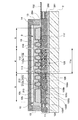
次に、本実施形態の表示装置1の具体的な態様を図2〜図4を参照して説明する。図2に本実施形態の表示装置の平面模式図を示し、図3には図2のA-A'線に沿う断面図を示し、図4には図2のB-B'線に沿う断面図を示す。
図2に示すように、本実施形態の表示装置1は、ガラス等からなる透明な基板2と、図示略のカレント薄膜トランジスタ(スイッチング素子)に接続された画素電極(第1電極)が基板2上にマトリックス状に配置されてなる図示略の画素電極領域(第1電極領域)と、画素電極領域の周囲に配置されるとともに各画素電極に接続される発光用電源配線103(103R、103G、103B)と、少なくとも画素電極領域上に位置する平面視略矩形の表示画素部3(図中一点鎖線の枠内)とを具備して構成されている。また表示画素部3は、中央部分の実表示領域4(図中二点鎖線の枠内)と、実表示領域4の周囲に配置されたダミー領域5(一点鎖線及び二点鎖線の間の領域)とに区画されている。
【0031】
また、実表示領域4の図中両側には、前述の走査線駆動回路105、105が配置されている。この走査線駆動回路105、105はダミー領域5の下側(基板側2)に位置して設けられている。更にダミー領域5の下側には、走査線駆動回路105、105に接続される走査線駆動回路用制御信号配線105aと走査線駆動回路用電源配線105bとが設けられている。
更に実表示領域4の図中上側には、前述の検査回路106が配置されている。この検査回路106はダミー領域5の下側(基板側2)に位置して設けられており、この検査回路106により、製造途中や出荷時の表示装置の品質、欠陥の検査を行うことができる。
【0032】
図2に示すように、発光用電源配線103R、103G、103Bは、ダミー画素領域5の周囲に配設されている。各発光用電源配線103R、103G、103Bは、基板2の図2中下側から走査線駆動回路用制御信号配線105bに沿って図2中上方に延在し、走査線駆動回路用電源配線105bが途切れた位置から折曲してダミー画素領域5の外側に沿って延在し、実表示領域4内にある図示略の画素電極に接続されている。
【0033】
また、基板2には、陰極12に接続される陰極配線12aが形成されている。この陰極配線12aは、発光用電源配線103R、103G、103Bを囲むように平面視略コ字状に形成されている。
【0034】
また基板2の一端には、ポリイミドテープ130が貼り付けられ、このポリイミドテープ130上に制御用IC131が実装されている。この制御用IC131には、図1に示したデータ側駆動回路104、陰極用電源回路131及び発光用電源回路132が内蔵されている。
【0035】
次に図3及び図4に示すように、基板2上には回路部11が形成され、この回路部11上に表示画素部3が形成されている。また基板2には、表示画素部3を環状に囲む封止材13が形成され、更に表示画素部3上に封止基板14が備えられている。封止基板14は、封止材13を介して基板2に接合されており、ガラス、金属若しくは樹脂等からなるものである。また封止基板14の裏側には、吸着剤15が貼り付けられ、表示画素部3と封止基板14の間の空間に混入した水又は酸素を吸収できるようになっている。尚、吸着剤15に代えてゲッター剤を用いても良い。また封止材13は、例えば熱硬化樹脂あるいは紫外線硬化樹脂からなるものであり、特に熱硬化樹脂の一種であるエポキシ樹脂よりなることが好ましい。
【0036】
回路部11の中央部分には、画素電極領域11aが設けられている。この画素電極領域11aには、カレント薄膜トランジスタ123と、このカレント薄膜トランジスタ123(スイッチング素子)に接続された画素電極111が備えられている。カレント薄膜トランジスタ123は、基板2上に積層された下地保護層281、第2層間絶縁層283及び第1層間絶縁層284に埋め込まれて形成され、また画素電極111は、第1層間絶縁層284上に形成されている。
【0037】
尚、回路部11には、前述した保持容量cap及びスイッチング薄膜トランジスタ142も形成されているが、図3及び図4ではこれらの図示を省略している。
【0038】
次に、図3において、画素電極領域11aの図中両側には、前述の走査線駆動回路105が設けられている。また、図4において、画素電極領域11aの図中左側には、前述の検査回路106が設けられている。
走査線駆動回路105には、シフトレジスタに含まれるインバータを構成するNチャネル型又はPチャネル型の薄膜トランジスタ105cが備えられ、この薄膜トランジスタ105cは、画素電極111に接続されていない点を除いて上記のカレント薄膜トランジスタ123と同様の構造とされている。
また検査回路106にも同様に、薄膜トランジスタ106aが備えられ、この薄膜トランジスタ106aも、画素電極111に接続されていない点を除いてカレント薄膜トランジスタ123と同様の構造とされている。
【0039】
また図3に示すように、走査線駆動回路105、105の図中外側の下地保護層281上には、走査線回路用制御信号配線105aが形成されている。更に走査線回路用制御信号配線105aの外側の第2層間絶縁層283上には、走査線回路用電源配線105bが形成されている。
更に図4に示すように、検査回路路106の図中左側の下地保護層281上には、検査回路用制御信号配線106bが形成されている。更に検査回路用制御信号配線106bの左側の第2層間絶縁層283上には、検査回路用電源配線106cが形成されている。
【0040】
また図3に示すように、走査線回路用電源配線105bの外側には、発光用電源配線103が形成されている。この発光用電源配線103は、2つの配線、あるいは異なる層に形成された導電部を利用した二重配線構造を採用しており、前述したように表示画素部3の外側に配置されている。二重配線構造を採用することで配線抵抗を軽減できる。
例えば、図3中左側にある赤色用の発光用電源配線103Rは、下地保護層281上に形成された第1配線103R1と、第2層間絶縁層283を介して第1配線103R1上に形成された第2配線103R2とから構成されている。第1配線103R1及び第2配線103R2は、図2に示すように第2層間絶縁層283を貫通するコンタクトホール103R3により接続されている。
このように、第1配線103R1は、陰極用配線12aと同じ階層位置に形成されており、第1配線103R1と陰極用配線12aとの間は第2層間絶縁層283が配置されている。このような構造をとることで、第1配線103R1と陰極用配線12aとの間に第2の静電容量C2が形成されている。
【0041】
同様に、図3の右側にある青色及び緑色用の発光用電源配線103G、103Bも二重配線構造を採用しており、それぞれ下地下地保護層281上に形成された第1配線103G1、103B1と、第2層間絶縁層283上に形成された第2配線103G2、103B2とから構成され、第1配線103G1、103B1及び第2配線103G2、103B2は、図2及び図3に示すように第2層間絶縁層283を貫通するコンタクトホール103G3、103B3により接続されている。そして、青色の第1配線103B1及び陰極用配線12aの間に第2の静電容量C2が形成されている。
【0042】
第1配線103R1・・・及び第2配線103R2・・・の間隔は、例えば、0.6〜1.0μmの範囲が好ましい。間隔が0.6μm未満だと、データ線と走査線のような異なる電位を有するソースメタルとゲートメタルの間の寄生容量が増える為、例えば画素内においては、数多くのソースメタルとゲートメタルのクロス部が存在することにより、データ信号(画像信号)配線遅延を引き起こす。その結果、定められた期間内にデータ信号(画像信号)を書き込む事が出来ない為、コントラストの低下を引き起こす。第1配線103R1・・・及び第2配線103R2・・・に挟まれる第2層間絶縁層283の材質は、例えばSiO2等が好ましが、1.0μm以上形成するとSiO2の応力により基板が割れる恐れが生じる。
【0043】
また、各発光用電源配線103R・・・の上側には、表示画素部3から延出した陰極12が形成されている。これにより、各発光用電源配線103R・・・の第2配線103R2・・・が、第1層間絶縁層284を挟んで陰極112と対向配置され、これにより第2配線103R2・・・と陰極12との間に前述の第1の静電容量C1が形成される。
【0044】
第2配線103R2・・・と陰極12の間隔は、例えば、0.6〜1.0μmの範囲が好ましい。間隔が0.6μm未満だと、画素電極とソースメタルのような異なる電位を有する画素電極とソースメタルの間の寄生容量が増える為、ソースメタルを用いているデータ線の配線遅延が生じる。その結果、定められた期間内にデータ信号(画像信号)を書き込む事が出来ない為、コントラストの低下を引き起こす。第2配線103R2・・・と陰極12に挟まれる第1層間絶縁層284の材質は、例えばSiO2やアクリル樹脂等が好ましい。しかし、SiO2を1.0μm以上形成すると応力により基板が割れる恐れが生じる。また、アクリル樹脂の場合は、2.0μm程度まで形成することができるが、水を含むを膨張する性質が有る為、その上に形成する画素電極を割る恐れがある。
また第1配線103R1・・・と陰極用配線12aの間隔は、例えば、4〜200μmの範囲が好ましい。間隔が4μm未満だと、現状では露光機の精度により配線同士がショートする可能性がある。第1配線103R2・・・と陰極用配線12aに挟まれる第2層間絶縁層283の材質は、例えばSiO2やアクリル樹脂等が好ましい。
【0045】
このように、本実施形態の表示装置1によれば、発光用電源配線103と陰極12との間に第1の静電容量C1が設けられるので、発光用電源配線103を流れる駆動電流の電位が変動した場合に第1の静電容量C1に蓄積された電荷が発光用電源配線103に供給され、駆動電流の電位不足分がこの電荷により補われて電位変動を抑制することができ、表示装置1の画像表示を正常に保つことができる。
特に、発光用電源配線103と陰極12とが表示画素部3の外側で対向するので、発光用電源配線103と陰極112との間隔を小さくして第1の静電容量C1に蓄積される電荷量を増大させることができ、駆動電流の電位変動をより小さくして画像表示を安定に行うことができる。
更に、本実施形態の表示装置1によれば、発光用電源配線103が第1配線及び第2配線からなる二重配線構造を有し、第1配線と陰極用配線との間に第2の静電容量C2が設けられているので、第2の静電容量C2に蓄積された電荷も発光用電源配線103に供給されるため、電位変動をより抑制することができ、表示装置1の画像表示をより正常に保つことができる。
【0046】
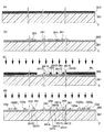
次に、カレント薄膜トランジスタ123を含む回路部11の構造を詳細に説明する。図5に、画素電極領域11aの要部断面図を示す。
図5に示すように、基板2の表面には、SiO2を主体とする下地保護層281が積層され、この下地保護層281上には島状のシリコン層241が形成されている。また、シリコン層241及び下地保護層281は、SiO2及び/又はSiNを主体とするゲート絶縁層282により被覆されている。そして、シリコン層241上には、ゲート絶縁層282を介してゲート電極242が形成されている。なお、このゲート電極242は走査線の一部である。
また、ゲート電極242及びゲート絶縁層282は、SiO2を主体とする第2層間絶縁層283によって被覆されている。なお、本明細書において、「主体」とする成分とは最も含有率の高い成分のことを言うものとする。
【0047】
次に、シリコン層241のうち、ゲート絶縁層282を介してゲート電極242と対向する領域がチャネル領域241aとされている。また、シリコン層241のうち、チャネル領域241aの図中右側には低濃度ソース領域241b及び高濃度ソース領域Sが設けられる一方、チャネル領域241aの図中左側には低濃度ドレイン領域241c及び高濃度ドレイン領域241Dが設けられており、いわゆるLDD(Light Doped Drain)構造が形成されている。カレント薄膜トランジスタ123は、このシリコン層241を主体として構成されている。
【0048】
高濃度ソース領域241Sは、ゲート絶縁層282と第2層間絶縁層283とに亙って開孔するコンタクトホール245を介して、第2層間絶縁層283上に形成されたソース電極243に接続されている。このソース電極243は、上述したデータ線の一部として構成される。一方、高濃度ドレイン領域241Dは、ゲート絶縁層282と第2層間絶縁層283とに亙って開孔するコンタクトホール246を介して、ソース電極243と同一層からなるドレイン電極244に接続されている。
【0049】
ソース電極243及びドレイン電極244が形成された第2層間絶縁層283上に第1層間絶縁層284が形成されている。そして、ITO等からなる透明な画素電極111が、この第1層間絶縁層284上に形成されるとともに、第1層間絶縁層284に設けられたコンタクトホール111aを介してドレイン電極244に接続されている。すなわち、画素電極111は、ドレイン電極244を介して、シリコン層241の高濃度ドレイン電極241Dに接続されている。
尚、図3に示すように、画素電極111は、実表示領域4に対応する位置に形成されているが、実表示領域4の周囲に形成されたダミー領域5には、画素電極111と同じ形態のダミー画素電極111'が設けられる。
このダミー画素電極111'は、高濃度ドレイン電極241Dに接続されない点を除き、画素電極111と同一の形態である。
【0050】
次に、表示画素部3の実画素領域4には、機能層110及びバンク112が形成されている。
機能層110は図3〜図5に示すように、画素電極111・・・上の各々に積層されている。またバンク112は、各画素電極111及び各機能層110の間に備えられており、各機能層110を区画している。
【0051】
バンク112は、基板2側に位置する無機物バンク層112aと基板2から離れて位置する有機物バンク層112bとが積層されて構成されている。尚、無機物バンク層112aと有機物バンク層112bとの間に遮光層を配置してもよい。
【0052】
無機質、有機物バンク層112a、112bは、画素電極111の周縁部上に乗上げて形成されており、また無機物バンク層112aは、有機物バンク層112bよりも画素電極111の中央側まで形成されている。
また、無機物バンク層112aは、例えば、SiO2、TiO2、SiN等の無機材料からなることが好ましい。また無機物バンク層112aの膜厚は、50〜200nmの範囲が好ましく、特に150nmがよい。膜厚が50nm未満では、無機物バンク層112aが後述する正孔注入/輸送層より薄くなり、正孔注入/輸送層の平坦性を確保できなくなるので好ましくない。また膜厚が200nmを越えると、無機物バンク層112aによる段差が大きくなって、正孔注入/輸送層上に積層する後述の発光層の平坦性を確保できなくなるので好ましくない。
【0053】
更に、有機物バンク層112bは、アクリル樹脂、ポリイミド樹脂等の通常のレジストから形成されている。この有機物バンク層112bの厚さは、0.1〜3.5μmの範囲が好ましく、特に2μm程度がよい。厚さが0.1μm未満では、後述する正孔注入/輸送層及び発光層の合計厚より有機物バンク層112bが薄くなり、発光層が上部開口部112dから溢れるおそれがあるので好ましくない。また、厚さが3.5μmを越えると、上部開口部112dによる段差が大きくなり、有機物バンク層112b上に形成する陰極12のステップガバレッジを確保できなくなるので好ましくない。また、有機物バンク層112bの厚さを2μm以上にすれば、陰極12と画素電極111との絶縁を高めることができる点でより好ましい。
このようにして、機能層110は、バンク112より薄く形成されている。
【0054】
また、バンク112の周辺には、親液性を示す領域と、撥液性を示す領域が形成されている。
親液性を示す領域は、無機物バンク層112a及び画素電極111であり、これらの領域には、酸素を反応ガスとするプラズマ処理によって水酸基等の親液基が導入されている。また、撥液性を示す領域は、有機物バンク層112bであり、4フッ化メタンを反応ガスとするプラズマ処理によってフッ素等の撥液基が導入されている。
【0055】
次に図5に示すように、機能層110は、画素電極111上に積層された正孔注入/輸送層110aと、正孔注入/輸送層110a上に隣接して形成された発光層110bとから構成されている。
正孔注入/輸送層110aは、正孔を発光層110bに注入する機能を有するとともに、正孔を正孔注入/輸送層110a内部において輸送する機能を有する。このような正孔注入/輸送層110aを画素電極111と発光層110bの間に設けることにより、発光層110bの発光効率、寿命等の素子特性が向上する。また、発光層110bでは、正孔注入/輸送層110aから注入された正孔と、陰極12からの電子とが結合して蛍光を発生させる。
【0056】
発光層110bは、赤色(R)に発光する赤色発光層、緑色(G)に発光する緑色発光層、及び青色(B)に発光する青色発光層の3種類を有し、図1及び図2に示すように、各発光層がストライプ配置されている。
【0057】
次に、表示画素部3のダミー領域5には、ダミー機能層210及びダミーバンク212が形成されている。
ダミーバンク212は、基板2側に位置するダミー無機物バンク層212aと基板2から離れて位置するダミー有機物バンク層212bとが積層されて構成されている。ダミー無機物バンク層212aは、ダミー画素電極111'の全面に形成されている。またダミー有機物バンク層212bは、有機物バンク層112bと同様に画素電極111の間に形成されている。
そして、ダミー機能層210は、ダミー無機物バンク212aを介してダミー画素電極111'上に形成されている。
【0058】
ダミー無機物バンク層212a及びダミー有機物バンク層121bは、先に説明した無機質、有機物バンク層112a、112bと同様の材質、同様の膜厚を有するものである。
また、ダミー機能層210は、図示略のダミー正孔注入/輸送層と図示略のダミー発光層とが積層されてなり、ダミー正孔注入/輸送層及びダミー発光層の材質や膜厚は、前述の正孔注入/輸送層110a及び発光層110bと同様である。
従って上記の機能層110と同様に、ダミー機能層210はダミーバンク212より薄く形成されている。
【0059】
ダミー領域5を実表示領域4の周囲に配置することにより、実表示領域4の機能層110の厚さを均一にすることができ、表示ムラを抑制することができる。即ち、ダミー領域5を配置することで、表示素子をインクジェット法によって形成する場合における吐出した組成物の乾燥条件を実表示領域4内で一定にすることができ、実表示領域4の周縁部で機能層110の厚さに偏りが生じるおそれがない。
【0060】
次に陰極12は、実表示領域4とダミー領域5の全面に形成されるとともにダミー領域5の外側にある基板2上まで延出され、ダミー領域5の外側、即ち表示画素部3の外側で発光用電源配線103と対向配置されている。
また陰極12の端部が、回路部11に形成された陰極用配線12aに接続されている。
陰極12は、画素電極111の対向電極として機能層110に電流を流す役割を果たす。この陰極12は、例えば、フッ化リチウムとカルシウムの積層体からなる第1陰極層12bと、第2陰極層12cとが積層されて構成されている。陰極12のうち、第2陰極層12cのみが表示画素部3の外側まで延出されている。
第2陰極層12cは、発光層110bから発した光を基板2側に反射させる機能をも有し、例えば、Al、Ag、Mg/Ag積層体等からなることが好ましい。
更に第2陰極層12b上にSiO2、SiN等からなる酸化防止用の保護層を設けても良い。
【0061】
次に本実施形態の表示装置の製造方法を図面を参照して説明する。
まず、図6ないし図8を参照して、基板2上に回路部11を形成する方法について説明する。なお、図6ないし図8に示す各断面図は、図2中のA−A'線のに沿う断面に対応している。なお、以下の説明において、不純物濃度は、いずれも活性化アニール後の不純物として表される。
【0062】
まず、図6(a)に示すように、基板2上に、シリコン酸化膜などからなる下地保護層281を形成する。次に、ICVD法、プラズマCVD法などを用いてアモルファスシリコン層を形成した後、レーザアニール法又は急速加熱法により結晶粒を成長させてポリシリコン層501とする。
【0063】
次に図6(b)に示すように、ポリシリコン層501をフォトリソグラフィ法によりパターニングして島状のシリコン層241,251及び261を形成し、更にシリコン酸化膜からなるゲート絶縁層282を形成する。
シリコン層241は、実表示領域4に対応する位置に形成されて画素電極111に接続されるカレント薄膜トランジスタ123(以下、「画素用TFT」と表記する場合がある)を構成するものであり、シリコン層251,261は、走査線駆動回路105内のPチャネル型及びNチャネル型の薄膜トランジスタ(以下、「駆動回路用TFT」と表記する場合がある)をそれぞれ構成するものである。
ゲート絶縁層282の形成は、プラズマCVD法、熱酸化法などにより、各シリコン層241、251、261及び下地保護層281を覆う厚さ約30nm〜200nmのシリコン酸化膜を形成することにより行う。ここで、熱酸化法を利用してゲート絶縁層282を形成する際には、シリコン層241,251及び261の結晶化も行い、これらのシリコン層をポリシリコン層とすることができる。チャネルドープを行う場合には、例えば、このタイミングで約1×1012cm−2のドーズ量でボロンイオンを打ち込む。その結果、シリコン層241,251及び261は、不純物濃度が約1×1017cm−3の低濃度P型のシリコン層となる。
【0064】
次に図6(c)に示すように、シリコン層241、261の一部にイオン注入選択マスクM1を形成し、この状態でリンイオンを約1×1015cm−2のドーズ量でイオン注入する。その結果、イオン注入選択マスクM1に対してセルフアライン的に高濃度不純物が導入され、シリコン層241及び261中に高濃度ソース領域241S及び261S並びに高濃度ドレイン領域241D及び261Dが形成される。
【0065】
次に図6(d)に示すように、イオン注入選択マスクM1を除去した後に、ゲート絶縁層282上にドープドシリコン、シリサイド膜、或いはアルミニウム膜やクロム膜、タンタル膜といった厚さ約500nm程度の金属膜を形成し、更にこの金属膜をパターニングすることにより、Pチャネル型の駆動回路用TFTのゲート電極252、画素用TFTのゲート電極242、Nチャネル型の駆動回路用TFTのゲート電極262を形成する。また、上記パターニングにより、走査線駆動回路用信号配線105a、発光用電源配線の第1配線103R1、103G1,103B1、陰極用配線12aの一部を同時に形成する。
【0066】
更に、ゲート電極242,252及び262をマスクとし、シリコン層241,251及び261に対してリンイオンを約4×1013cm−2のドープ量でイオン注入する。その結果、ゲート電極242,252及び262に対してセルフアライン的に低濃度不純物が導入され、図6(d)に示すように、シリコン層241及び261中に低濃度ソース領域241b及び261b、並びに低濃度ドレイン領域241c及び261cが形成される。また、シリコン層251中に低濃度不純物領域251S及び251Dが形成される。
【0067】
次に図7(a)に示すように、ゲート電極252の周辺を除く全面にイオン注入選択マスクM2を形成する。このイオン注入選択マスクM2を用いて、シリコン層251に対してボロンイオンを約1.5×1015cm−2のドープ量でイオン注入する。結果として、ゲート電極252もマスクとして機能し、シリコン層252中にセルフアライン的に高濃度不純物がドープされる。これにより251S及び251Dがカウンタードープされ、P型チャネル型の駆動回路用TFTのソース領域及びドレイン領域となる。
次に図7(b)に示すように、イオン注入選択マスクM2を除去した後に、基板2の全面に第2層間絶縁層283を形成し、更にフォトリソグラフィ法により第2層間絶縁層283をパターニングして、各TFTのソース電極及びドレイン電極並びに陰極用配線12aに対応する位置にコンタクトホール形成用の孔H1を設ける。
【0068】
次に図7(c)に示すように、第2層間絶縁層283を覆うように、アルミニウム、クロム、タンタル等の金属からなる厚さ約200nmないし800nm程度の導電層504を形成することにより、先に形成した孔H1にこれらの金属を埋め込んでコンタクトホールを形成する。更に導電層504上にパターニング用マスクM3を形成する。
次に図8(a)に示すように、導電層504をパターニング用マスクM3によってパターニングし、各TFTのソース電極243,253,263、ドレイン電極244及び254、各発光用電源配線の第2配線103R2、103G2、103B2、走査線回路用電源配線105b及び陰極用配線12aを形成する。
上記のように、第1配線103R1及び103B1を陰極用配線12aと同じ階層に離間して形成することで、第2の静電容量C2が形成される。
【0069】
次に図8(b)に示すように、第2層間絶縁層283を覆う第1層間絶縁層284を、例えばアクリル系などの樹脂材料によって形成する。この第1層間絶縁層284は、約1〜2μm程度の厚さに形成されることが望ましい。
次に図8(c)に示すように、第1層間絶縁層284のうち、画素用TFTのドレイン電極244に対応する部分をエッチングによって除去してコンタクトホール形成用の孔H2を形成する。このとき、同時に陰極用配線12a上の第1層間絶縁層284も除去する。このようにして、基板2上に回路部11が形成される。
【0070】
次に、図9を参照して、回路部11上に表示画素部3を形成することにより表示装置1を得る手順について説明する。図9に示す断面図は、図2中のA−A'線に沿う断面に対応している。
まず図9(a)に示すように、基板2の全面を覆うようにITO等の透明電極材料からなる薄膜を形成し、当該薄膜をパターニングすることにより、第1層間絶縁層284に設けた孔H2を埋めてコンタクトホール111aを形成するとともに画素電極111及びダミー画素電極111'を形成する。画素電極111は、カレント薄膜トランジスタ123の形成部分のみに形成され、コンタクトホール111aを介してカレント薄膜トランジスタ123(スイッチング素子)に接続される。尚、ダミー電極111'は島状に配置される。
【0071】
次に、図9(b)に示すように、第1層間絶縁層284及び画素電極111及びダミー画素電極111'上に無機物バンク層112a及びダミー無機物バンク層212aを形成する。無機物バンク層112aは、画素電極111の一部が開口する態様にて形成し、ダミー無機物バンク層212aはダミー画素電極111'を完全に覆うように形成する。
無機物バンク層112a及びダミー無機物バンク層212aは、例えばCVD法、TEOS法、スパッタ法、蒸着法等によって第1層間絶縁層284及び画素電極111の全面にSiO2、TiO2、SiN等の無機質膜を形成した後に、当該無機質膜をパターニングすることにより形成する。
【0072】
更に図9(b)に示すように、無機物バンク層112a及びダミー無機物バンク層212a上に、有機物バンク層112b及びダミー有機物バンク層212bを形成する。有機物バンク層は112bは、無機物バンク層112aを介して画素電極111の一部が開口する態様にて形成し、ダミー有機物バンク層212bはダミー無機物バンク層212aの一部が開口する態様にて形成する。このようにして、第1層間絶縁層284上にバンク112を形成する。
【0073】
続いて、バンク112の表面に、親液性を示す領域と、撥液性を示す領域を形成する。本実施例においてはプラズマ処理工程により、各領域を形成するものとしている。具体的に該プラズマ処理工程は、画素電極111、無機物バンク層112a及びダミー無機物バンク層212aを親液性にする親液化工程と、有機物バンク層112b及びダミー有機物バンク層212bを撥液性にする撥液化工程とを少なくとも具備している。
【0074】
すなわち、バンク112を所定温度(例えば70〜80℃程度)に加熱し、次いで親液化工程として大気雰囲気中で酸素を反応ガスとするプラズマ処理(O2プラズマ処理)を行う。続いて、撥液化工程として大気雰囲気中で4フッ化メタンを反応ガスとするプラズマ処理(CF4プラズマ処理)を行い、プラズマ処理のために加熱されたバンク112を室温まで冷却することで、親液性及び撥液性が所定箇所に付与されることとなる。
【0075】
更に、画素電極111上及びダミー無機物バンク層212a上にそれぞれ、機能層110並びにダミー機能層210をインクジェット法により形成する。機能層110並びにダミー機能層210は、正孔注入/輸送層材料を含む組成物インクを吐出・乾燥した後に、発光層材料を含む組成物インクを吐出・乾燥することにより形成される。なお、この機能層110及びダミー機能層210の形成工程以降は、正孔注入/輸送層及び発光層の酸化を防止すべく、窒素雰囲気、アルゴン雰囲気等の不活性ガス雰囲気で行うことが好ましい。
【0076】
次に、図9(c)に示すように、バンク112及び機能層110並びにダミー機能層210を覆う陰極12を形成する。陰極12は、バンク112及び機能層110並びにダミー機能層210上に第1陰極層12bを形成した後に、第1陰極層12bを覆って基板2上の陰極用配線12aに接続される第2陰極層12cを形成することにより得られる。
このように、第2陰極層12cを陰極用配線12aに接続させるべく第2陰極層12cを表示画素部3から基板2上に延出させることにより、第2陰極層12cが第1層間絶縁層284を介して発光用電源線103に対向配置され、第2陰極層12c(陰極)と発光用電源線103との間に第1の静電容量C1が形成される。
【0077】
最後に、基板2にエポキシ樹脂等の封止材13を塗布し、この封止材13を介して基板2に封止基板14を接合する。このようにして、図1〜図4に示すような表示装置1が得られる。
【0078】
[第2の実施形態]
以下、本発明の第2の実施形態を図面を参照して説明する。本実施形態は、本発明の一態様を示すものであり、この発明を限定するものではなく、本発明の技術的思想の範囲内で任意に変更可能である。なお、以下に示す各図においては、各層や各部材を図面上で認識可能な程度の大きさとするため、各層や各部材ごとに縮尺を異ならせてある。
【0079】
図10及び図11に、本実施形態の表示装置101の具体的な態様を示す。図10には本実施形態の表示装置の平面模式図を示し、図11には図10のA-A'線に沿う断面図を示す。なお、図10及び図11に示す構成要素のうち、前述の図2及び図3に示した構成要素と同一の構成要素には同一符号を付してその説明を省略あるいは簡単に説明する。
【0080】
図10に示すように、本実施形態の表示装置101は、基板2と、基板2上に複数の画素電極(第1電極)がマトリックス状に配置されてなる図示略の画素電極領域(第1電極領域)と、画素電極領域の周囲に配置される発光用電源配線213(213R、213G、213B)と、少なくとも画素電極領域上に位置する平面視略矩形の表示画素部203(図中一点鎖線の枠内)とを具備して構成されている。また表示画素部203は、中央部分の実表示領域204(図中二点鎖線の枠内)と、実表示領域204の周囲に配置されたダミー領域205(一点鎖線及び二点鎖線の間の領域)とに区画されている。
【0081】
また、実表示領域204の図中両側であってダミー領域205の下側(基板側2)には、走査線駆動回路105、105が配置されている。更にダミー領域205の下側には、走査線駆動回路105、105に接続される走査線駆動回路用制御信号配線105aと、走査線駆動回路用電源配線105bとが設けられている。
更に実表示領域204の図中上側であってダミー領域205の下側(基板側2)には、検査回路106が配置されている。
【0082】
また、発光用電源配線213R、213G、213Bについても、ダミー画素領域205の下側に配設されている。各発光用電源配線213R、213G、213Bは、基板2の図中下側から走査線駆動回路用電源配線105bに沿って図中上方に延在し、走査線駆動回路用電源配線105bが途切れた位置から折曲して、実表示領域204内にある図示略の画素電極に接続されている。
このように、本実施形態では、第1の実施形態と異なり、ダミー領域205が、発光用電源配線213上まで形成されている。
【0083】
次に図11に示すように、基板2上には回路部11が形成され、この回路部11上に表示画素部203が形成されている。また基板2には封止材13が形成され、更に表示画素部203上に封止基板14が備えられている。
【0084】
回路部11の中央部分には、画素電極領域11aが設けられている。画素電極領域11aには、カレント薄膜トランジスタ123(スイッチング素子)と、このカレント薄膜トランジスタ123に接続された画素電極111が備えられている。
また、画素電極領域11aの周囲には、ダミー画素電極111'が形成されている。
【0085】
次に、図11において、画素電極領域11aの図中両側には、前述の走査線駆動回路105が設けられている。
走査線駆動回路105には、シフトレジスタに含まれるインバータを構成するNチャネル型又はPチャネル型の薄膜トランジスタ105cが備えられている。
また、走査線駆動回路105、105の図中外側の下地保護層281上には、走査線回路信号配線105aが形成され、第2層間絶縁層283上には、走査線回路電源配線105bが形成されている。
【0086】
次に陰極222(第2電極)は、実表示領域204とダミー領域205の全面に形成されるとともにその端部がダミー領域205の外側にある基板2上まで延出され、この陰極222の端部が、回路部11に形成された陰極用配線222a(第2電極用配線)に接続されている。
陰極222は、画素電極111の対向電極として機能層110に電流を流す役割を果たす。この陰極222は、例えば、第1陰極層222bと第2陰極層222cとが積層されて構成されている。陰極222のうち、第2陰極層222cのみが表示画素部3の外側まで延出されている。
第1、第2陰極層222b、222cの構成材料及び膜厚は、先に説明した第1、第2陰極層12b、12cと同様である。
【0087】
次に、走査線回路電源配線105bの外側には、発光用電源配線213が設けられている。この発光用電源配線213は、前述したようにダミー領域205の下側に配置されている。
ダミー領域205には、ダミー無機物バンク層212aを介してダミー画素電極111'上に形成されたダミー機能層210と、ダミー機能層210・・・の間に形成されたダミーバンク212とが備えられている。ダミー機能層210はダミーバンク212より薄く形成されている。そして、各発光用電源配線103は、ダミー機能層210を挟んで陰極222と対向する位置に配置されている。即ち各発光用電源配線103は、ダミーバンク212の間に対応する位置に配置されている。
またダミーバンク212の間には、画素電極111及びダミー機能層210に加えて陰極222の一部が配置されており、これにより陰極222と各発光用電源配線103とが第1層間絶縁層284、画素電極111、ダミー無機物バンク層212a及びダミー機能層210を介して対向している。
ダミー機能層210がダミーバンク212より薄く形成されているので、ダミー機能層210上にある陰極222がダミーバンク212上にある陰極222よりも発光用電源配線213側に接近して配置されている。
このように、陰極222と各発光用電源配線103とが、ダミー機能層210を介して対向することにより、第1の静電容量C1が形成される。
尚、各発光用電源配線103が、ダミーバンク212と対向する位置に配置されると、陰極222と各発光用電源配線103がダミーバンク212を介して対向することになり、陰極222と各発光用電源配線103との間隔が大きくなり、静電容量が形成されなくなるので好ましくない。
【0088】
また発光用電源配線213は、2つの配線からなる二重配線構造を採用している。
即ち、例えば図11の左側にある赤色用の発光用電源配線213Rは、下地下地保護層281上に形成された第1配線213R1と、第2層間絶縁層283上に形成された第2配線213R2とから構成されている。第1配線213R1及び第2配線213R2は、図10に示すように第2層間絶縁層283を貫通するコンタクトホール213R3により接続されている。
このように、第1配線203R1は、陰極用配線222aと同じ階層位置に形成されており、第1配線203R1と陰極用配線222aとの間は第2層間絶縁層283が配置されている。このような構造をとることで、第1配線203R1と陰極用配線222aとの間に第2の静電容量C2が形成されている。
【0089】
同様に、図11の右側にある青色及び緑色用の発光用電源配線213G、213B、213Rも二重配線構造を採用しており、それぞれ下地下地保護層281上に形成された第1配線213G1、213B1と、第2層間絶縁層283上に形成された第2配線213G2、213B2とから構成され、第1配線213G1、213B1及び第2配線213G2、213B2は、図2及び図3に示すように第2層間絶縁層283を貫通するコンタクトホール213G3、213B3により接続されている。
そして、青色の第1配線213B1と陰極配線222aとの間に第2の静電容量C2が形成されている。
【0090】
第2配線203R2・・・と陰極222の間隔は、例えば、0.6〜1.0μmの範囲が好ましい。間隔が0.6μm未満だと、画素電極とソースメタルのような異なる電位を有する画素電極とソースメタルの間の寄生容量が増える為、ソースメタルを用いているデータ線の配線遅延が生じる。その結果、定められた期間内にデータ信号(画像信号)を書き込む事が出来ない為、コントラストの低下を引き起こす。第2配線203R2・・・と陰極222に挟まれる第1層間絶縁層284の材質は、例えばSiO2やアクリル樹脂等が好ましい。しかし、SiO2を1.0μm以上形成すると応力により基板が割れる恐れが生じる。また、アクリル樹脂の場合は、2.0μm程度まで形成することができるが、水を含むを膨張する性質が有る為、その上に形成する画素電極を割る恐れがある。
また第1配線103R1・・・と陰極用配線12aの間隔は、例えば、4〜200μmの範囲が好ましい。間隔が4μm未満だと、現状では露光機の精度により配線同士がショートする可能性がある。第1配線103R2・・・と陰極用配線12aに挟まれる第2層間絶縁層283の材質は、例えばSiO2やアクリル樹脂等が好ましい。
【0091】
このように、本実施形態の表示装置101によれば、第1の実施形態の表示装置1と同じ効果が得られる他に、以下の効果が得られる。
即ち、本実施形態の表示装置101によれば、実表示領域204を囲むダミー領域205が設けられ、発光用電源配線213がダミー機能層210を挟んで陰極222と対向するように配置されるため、発光用電源配線213がこのダミー領域205の下側に位置することになり、発光用電源配線213の配置スペースを発光素子部210の外側に新たに設ける必要がなく、これにより実表示領域204の占有面積を相対的に拡大することができる。
【0092】
[第3の実施形態]
次に、前記の第1または第2の実施形態の表示装置のいずれかを備えた電子機器の具体例について説明する。
図12(a)は、携帯電話の一例を示した斜視図である。図12(a)において、符号600は携帯電話本体を示し、符号601は前記の表示装置1,101のいずれかを用いた表示部を示している。
図12(b)は、ワープロ、パソコンなどの携帯型情報処理装置の一例を示した斜視図である。図12(b)において、符号700は情報処理装置、符号701はキーボードなどの入力部、符号703は情報処理装置本体、符号702は前記の表示装置1、101のいずれかを用いた表示部を示している。
図12(c)は、腕時計型電子機器の一例を示した斜視図である。図12(c)において、符号800は時計本体を示し、符号801は前記の表示装置1,101のいずれかを用いた表示部を示している。
図12(a)〜(c)に示すそれぞれの電子機器は、前記の第1または第2の実施形態の表示装置1、101のいずれかを用いた表示部を備えたものであり、先の第1または第2実施形態の表示装置の特徴を有するので、いずれの表示装置を用いても、表示品質に優れ、画像表示を安定に行うことができる電子機器となる。
【0093】
【発明の効果】
以上、詳細に説明したように、本発明の表示装置によれば、発光用電源配線と第2電極との間に第1の静電容量が設けられているので、発光用電源配線を流れる駆動電流の電位が変動した場合でも、第1の静電容量に蓄積された電荷が発光用電源配線に供給されるので、駆動電流の電位不足分がこの蓄積電荷により補われて電位変動を抑制することができ、表示装置の画像表示を正常に保つことができる。
【0094】
更に本発明の表示装置によれば、前記発光用電源配線が第1配線及び第2配線から構成され、これら第1配線と第2電極用配線との間に第2の静電容量が設けられるので、発光用電源配線を流れる駆動電流の電位が変動した場合に、第2の静電容量に蓄積された電荷が発光用電源配線に供給されて電位変動を抑制することができ、表示装置の画像表示をより正常に保つことができる。
【図面の簡単な説明】
【図1】 本発明の第1の実施形態の表示装置の配線構造を示す平面模式図。
【図2】 本発明の第1の実施形態の表示装置を示す平面模式図。
【図3】 図2のA-A'線に沿う断面図。
【図4】 図2のB-B'線に沿う断面図。
【図5】 本発明の第1の実施形態の表示装置の要部を示す断面図。
【図6】 本発明の第1の実施形態の表示装置の製造方法を説明する工程図。
【図7】 本発明の第1の実施形態の表示装置の製造方法を説明する工程図。
【図8】 本発明の第1の実施形態の表示装置の製造方法を説明する工程図。
【図9】 本発明の第1の実施形態の表示装置の製造方法を説明する工程図。
【図10】 本発明の第2の実施形態の表示装置を示す平面模式図。
【図11】 図10のA-A'線に沿う断面図。
【図12】 本発明の第3の実施形態である電子機器を示す斜視図。
【図13】 従来の表示装置の配線構造を示す平面模式図。
【符号の説明】
1 表示装置
2 基板
3 表示画素部
4、204 実表示領域
5、205 ダミー領域
11 回路部
11a 画素電極領域(第1電極領域)
12、222 陰極(第2電極)
12a、222a 陰極用配線(第2電極用配線)
103 発光用電源配線
103R1、103G1、103B1 第1配線
103R2、103G2、103B2 第2配線
110 機能層
110a 正孔注入/輸送層
110b 発光層
111 画素電極(第1電極)
112 バンク
123 カレント薄膜トランジスタ(スイッチング素子)
210 ダミー機能層(ダミー領域における機能層)
212 ダミーバンク(ダミー領域におけるバンク)
283 第2層間絶縁層(絶縁層)
284 第1層間絶縁層(絶縁層)
600 携帯電話本体(電子機器)
700 情報処理装置(電子機器)
800 時計本体(電子機器)
C1 第1の静電容量
C2 第2の静電容量[0001]
BACKGROUND OF THE INVENTION
The present invention relates to a display device and an electronic device each including an organic electroluminescent material.
[0002]
[Prior art]
In recent years, a color display device having a structure in which a light emitting layer made of a light emitting material such as an organic fluorescent material is sandwiched between a pixel electrode (anode) and a cathode, particularly an organic material using an organic electroluminescence (organic EL) material as the light emitting material. An EL display device has been developed.
As a driving method of such an organic EL display device, a scanning line in the row direction and a data line in the column direction are arranged in a matrix, and a capacitance element and a transistor are provided for each pixel of the EL element at the intersection. And so on, and so-called active matrix driving method is known in which light emission is continued until the next rewriting according to the voltage charged in the capacitance element of each pixel during writing scanning (see, for example, Patent Document 1). .
[0003]
FIG. 13 shows a wiring structure of a conventional display device. In the conventional display device, a plurality of
[0004]
Each
Further, each of the pixel regions A has a switching
[0005]
The light-emitting
The light emission
[0006]
According to such a configuration, when the
[Patent Document 1]
International Publication No. WO 98/3640 pamphlet.
[0007]
[Problems to be solved by the invention]
Incidentally, in order to cause the
However, in the conventional display device, since a relatively large driving current is required to cause the
[0008]
The present invention has been made in view of the above circumstances, and a display device that can stably perform image display by stabilizing the potential of a driving current applied from a light-emitting power supply wiring to a pixel electrode, and the display device It is an object of the present invention to provide an electronic device comprising:
[0009]
[Means for Solving the Problems]
To achieve the above objective,An organic EL device according to an embodiment of the present invention includes: a first electrode region in which a plurality of switching elements and a plurality of first electrodes connected to the switching elements are arranged in a matrix on the substrate; A functional layer formed above one electrode;
A light-emitting power supply line electrically connected to the first electrode through the switching element and having a first portion and a second portion; and provided in common to the plurality of first electrodes; and , A second electrode provided so as to partially overlap the power supply wiring for light emission, a cathode wiring electrically connected to the second electrode, and a second electrode formed so as to cover the second part A first insulating film; and a second insulating film formed to cover the first portion and a part of the cathode wiring; and between the first portion and the cathode wiring and the first The second insulating film is disposed between the portion and the second portion, and the first portion is formed in the same layer as a part of the cathode wiring along a part of the cathode wiring. And the second portion is formed through the contact hole formed in the second insulating film. 1 is electrically connected to the first portion, and is disposed to face a part of the second electrode with the first insulating film interposed between the second portion and the second electrode. It is characterized by.
The organic EL device according to an embodiment of the present invention is characterized in that the first portion and a part of the cathode wiring are formed by patterning the same metal film.
The organic EL device of the present invention includes a switching element and a first electrode region in which a plurality of first electrodes connected to the switching element are arranged in a matrix on a substrate, and above the first electrode. A light emitting power supply wiring for electrically connecting the formed functional layer, a light emitting power supply circuit and the first electrode via the switching element, and a common to the plurality of first electrodes, and A second electrode provided so as to partially overlap the power supply wiring for light emission, the power supply wiring for light emission is disposed in the first electrode region, and the first electrode is interposed via the switching element. And a first portion connected between the outer periphery of the substrate and the first electrode region, and a second portion connected to the first portion. Between the second part of the wiring and the second electrode Provided insulating film is characterized in that there is a first portion and a thin portion as compared with the provided insulating film between the second electrode of the light-emitting power source wiring.
The organic EL device according to the present invention is the organic EL device described above, and is provided between the second portion and the second electrode of the light-emitting power supply wiring, and the first portion. And the first insulating film provided between the first electrode and the second electrode, and the functional layer, and provided between the first portion of the light-emitting power supply wiring and the second electrode And a second insulating film.
The organic EL device of the present invention is the organic EL device described above, further including a dummy region provided between an outer periphery of the substrate and the first electrode region, wherein the functional layer includes the first layer. The first electrode region is provided above the first electrode, and the dummy region is provided between the second portion of the light-emitting power supply wiring and the second electrode, and an insulating film includes the functional layer. In addition to partitioning, the light-emitting power supply wiring is provided between the first portion and the second electrode.
The organic EL device of the present invention is the organic EL device described above, wherein a third electrode that is not connected to the switching element is provided below the functional layer in the dummy region. Features.
Moreover, the organic EL device of the present invention is the organic EL device described above, wherein the functional layer is formed thinner than the insulating film.
In the display device of the present invention, the first electrode connected to the switching element is arranged in a matrix on the substrate, the first electrode region is arranged around the first electrode region, and is connected to the first electrode. A light emitting power supply wiring and a functional layer formed above the first electrode, wherein at least a part of the second electrode is formed above the functional layer, the light emitting power supply wiring and the first electrode A first capacitance is provided between the two electrodes.
[0010]
According to such a display device, since the first capacitance is provided between the light emitting power supply wiring and the second electrode, even if the potential of the driving current flowing through the light emitting power supply wiring fluctuates, the first capacitance is provided. The electric charge accumulated in the electrostatic capacity is supplied to the light-emitting power supply wiring, so that the insufficient electric potential of the drive current is compensated by the accumulated charge, and the potential fluctuation can be suppressed, so that the image display of the display device is normal. Can be kept in.
[0011]
The display device according to the present invention is the display device described above, wherein the light emitting power supply wiring and the second electrode are opposed to each other outside the first electrode region, whereby the first electrostatic capacitance is provided. Is formed.
[0012]
According to such a display device, since the light-emitting power supply wiring faces the second electrode outside the first electrode region, the distance between the light-emitting power supply wiring and the second electrode is reduced and stored in the first capacitance. The amount of stored charge that is generated can be increased, and the potential variation of the drive current can be further reduced to stably display an image.
[0013]
In the display device of the present invention, it is preferable that a first interlayer insulating layer is disposed between the light-emitting power supply wiring and the second electrode.
[0014]
The display device of the present invention is the display device described above, and includes an actual display region formed by the first electrode, and a dummy region that is arranged around the actual display region and does not contribute to display. The second electrode is formed so as to cover at least the actual display region and the dummy region, and the light-emitting power supply wiring is disposed opposite to the second electrode with at least the dummy region interposed therebetween. Thus, the first capacitance is formed.
[0015]
According to such a display device, the dummy area surrounding the actual display area is provided, and the light emitting power supply wiring is disposed so as to face the second electrode across the dummy area. Therefore, it is not necessary to newly provide an arrangement space for the light-emitting power supply wiring outside the light-emitting element portion, and the occupied area of the actual display region can be relatively enlarged.
[0016]
In the display device of the present invention, it is preferable that the thickness of the functional layer in the dummy region is smaller than the thickness of the bank in the dummy region.
As a result, the second electrode on the functional layer in the dummy area is configured to be closer to the light-emitting power supply wiring side than the second electrode on the bank in the dummy area. The amount can be increased, and the potential fluctuation of the drive current can be further reduced to stably display an image.
[0017]
In the display device of the present invention, it is preferable that the first interlayer insulating layer is disposed between the light emitting power supply wiring and the functional layer in the dummy region.
[0018]
The display device of the present invention is the display device described above, wherein the light-emitting power supply wiring includes a first wiring and a second wiring facing each other with a second interlayer insulating layer interposed therebetween, and One wiring is formed at the same hierarchical position as the second electrode wiring, and a second capacitance is formed between the first wiring and the second electrode wiring. .
According to such a display device, since the second capacitance is provided between the first wiring and the second electrode wiring, when the potential of the driving current flowing through the light-emitting power supply wiring fluctuates, The electric charge accumulated in the capacitance of 2 is supplied to the light-emitting power supply wiring, so that the potential fluctuation can be suppressed, and the image display of the display device can be kept more normal.
[0019]
The display device of the present invention is the display device described above, wherein the functional layer is composed of a hole injection / transport layer and an organic electroluminescent material formed adjacent to the hole injection / transport layer. It is characterized by comprising a light emitting layer.
[0020]
According to such a display device, the functional layer includes a hole injection / transport layer and a light emitting layer. By applying a drive current with little potential fluctuation to the functional layer, high brightness and accurate color display can be achieved. It can be carried out.
[0021]
Next, in the display device of the present invention, the first electrode connected to the switching element is disposed on the substrate, the first electrode region is disposed around the first electrode region, and is connected to the first electrode. A light emitting power supply wiring, a functional layer and a second electrode are formed on each of the first electrodes, and a first interlayer insulating layer is formed on the light emitting power supply wiring. It is characterized by.
[0022]
The display device according to the present invention is the display device described above, wherein the light-emitting power supply wiring and the second electrode are outside the display pixel portion formed by the first electrode. The first capacitance is formed by facing each other across the layers.
The display device of the present invention is the display device described above, and has an actual display region formed by the first electrode and a dummy region that is arranged around the actual display region and does not contribute to display. The second electrode is formed so as to cover at least the actual display region and the dummy region, and the light-emitting power supply wiring is disposed opposite to the second electrode with at least the dummy region interposed therebetween, The first interlayer insulating layer is formed in the dummy region.
[0023]
The display device according to the present invention is the display device described above, wherein the thickness of the functional layer in the dummy region is smaller than the thickness of the bank in the dummy region.
The display device of the present invention is the display device described above, wherein the light-emitting power supply wiring includes a first wiring and a second wiring facing each other with a second interlayer insulating layer interposed therebetween, and The first wiring is formed at the same hierarchical position as the second electrode wiring, and a second capacitance is formed between the first wiring and the second electrode wiring. To do.
The display device of the present invention is the display device described above, wherein the functional layer is formed of a hole injection / transport layer and an organic electroluminescent material formed adjacent to the hole injection / transport layer. And a light emitting layer.
Next, an electronic apparatus according to the present invention includes any one of the display devices described above. According to such an electronic device, image display can be performed stably.
[0024]
DETAILED DESCRIPTION OF THE INVENTION
[First Embodiment]
A first embodiment of the present invention will be described below with reference to the drawings. This embodiment shows one aspect of the present invention, and does not limit the present invention, and can be arbitrarily changed within the scope of the technical idea of the present invention. In each of the drawings shown below, the scale of each layer and each member is different in order to make each layer and each member recognizable on the drawing.
[0025]
FIG. 1 is a schematic plan view of the wiring structure of the display device of this embodiment.
A
1 includes a plurality of
[0026]
A data
Further, each pixel region A has a switching
[0027]
The
The light emitting
[0028]
In addition, first capacitances C1,... Are formed between the
[0029]
In the
[0030]
Next, specific modes of the
As shown in FIG. 2, the
[0031]
Further, the scanning
Further, the above-described
[0032]
As shown in FIG. 2, the light-emitting
[0033]
Further, a
[0034]
A
[0035]
Next, as shown in FIGS. 3 and 4, the
[0036]
A
[0037]
The
[0038]
Next, in FIG. 3, the above-described scanning
The scanning
Similarly, the
[0039]
As shown in FIG. 3, a scanning line circuit
Further, as shown in FIG. 4, an inspection circuit
[0040]
Further, as shown in FIG. 3, a light emission
For example, the red light-emitting
Thus, the first wiring 103R1 is formed at the same hierarchical position as the
[0041]
Similarly, the light-emitting
[0042]
The distance between the first wiring 103R1... And the second wiring 103R2... Is preferably in the range of 0.6 to 1.0 μm, for example. If the distance is less than 0.6 μm, the parasitic capacitance between the source metal and the gate metal having different potentials such as the data line and the scanning line increases. The presence of the portion causes a data signal (image signal) wiring delay. As a result, a data signal (image signal) cannot be written within a predetermined period, which causes a decrease in contrast. The material of the second
[0043]
Further, a
[0044]
The distance between the second wiring 103R2... And the
The distance between the first wiring 103R1... And the
[0045]
As described above, according to the
In particular, since the light-emitting
Furthermore, according to the
[0046]
Next, the structure of the
As shown in FIG. 5, the surface of the
The
[0047]
Next, in the
[0048]
The high-
[0049]
A first
As shown in FIG. 3, the
The
[0050]
Next, a
As shown in FIGS. 3 to 5, the
[0051]
The
[0052]
The inorganic and
The
[0053]
Furthermore, the
In this way, the
[0054]
In addition, a region showing lyophilicity and a region showing liquid repellency are formed around the
The lyophilic regions are the
[0055]
Next, as shown in FIG. 5, the
The hole injection /
[0056]
The
[0057]
Next, a dummy
The
The dummy
[0058]
The dummy
The dummy
Therefore, similar to the
[0059]
By disposing the
[0060]
Next, the
The end of the
The
The
Furthermore, SiO2 is formed on the second cathode layer 12b.2An anti-oxidation protective layer made of SiN or the like may be provided.
[0061]
Next, a method for manufacturing the display device of this embodiment will be described with reference to the drawings.
First, a method for forming the
[0062]
First, as shown in FIG. 6A, a base
[0063]
Next, as shown in FIG. 6B, the
The
The
[0064]
Next, as shown in FIG. 6C, an ion implantation selection mask M1 is formed on a part of the silicon layers 241 and 261, and in this state, phosphorus ions are implanted at a dose of about 1 × 10 15 cm −2. As a result, high-concentration impurities are introduced in a self-aligned manner with respect to the ion implantation selection mask M1, and high-
[0065]
Next, as shown in FIG. 6D, after removing the ion implantation selection mask M1, a thickness of about 500 nm such as doped silicon, silicide film, aluminum film, chromium film, or tantalum film is formed on the
[0066]
Further, using the
[0067]
Next, as shown in FIG. 7A, an ion implantation
Next, as shown in FIG. 7B, after removing the ion implantation selection mask M2, a second
[0068]
Next, as shown in FIG. 7C, a
Next, as shown in FIG. 8A, the
As described above, the second capacitance C2 is formed by forming the first wirings 103R1 and 103B1 apart from each other in the same layer as the
[0069]
Next, as shown in FIG. 8B, a first
Next, as shown in FIG. 8C, a portion corresponding to the
[0070]
Next, a procedure for obtaining the
First, as shown in FIG. 9A, a thin film made of a transparent electrode material such as ITO is formed so as to cover the entire surface of the
[0071]
Next, as shown in FIG. 9B, the
The
[0072]
Further, as shown in FIG. 9B, the
[0073]
Subsequently, a region showing lyophilicity and a region showing liquid repellency are formed on the surface of the
[0074]
That is, the
[0075]
Furthermore, the
[0076]
Next, as shown in FIG. 9C, the
In this way, the
[0077]
Finally, a sealing
[0078]
[Second Embodiment]
Hereinafter, a second embodiment of the present invention will be described with reference to the drawings. This embodiment shows one aspect of the present invention, and does not limit the present invention, and can be arbitrarily changed within the scope of the technical idea of the present invention. In each of the drawings shown below, the scale of each layer and each member is different in order to make each layer and each member recognizable on the drawing.
[0079]
10 and 11 show specific modes of the
[0080]
As shown in FIG. 10, the
[0081]
Further, scanning
Further, an
[0082]
Further, the light-emitting
As described above, in the present embodiment, unlike the first embodiment, the
[0083]
Next, as shown in FIG. 11, the
[0084]
A
Further, a
[0085]
Next, in FIG. 11, the scanning
The scan
Further, the scanning line
[0086]
Next, the cathode 222 (second electrode) is formed on the entire surface of the
The
The constituent materials and film thicknesses of the first and second cathode layers 222b and 222c are the same as those of the first and second cathode layers 12b and 12c described above.
[0087]
Next, a light emitting
The
In addition to the
Since the dummy
As described above, the
When each light-emitting
[0088]
The light-emitting
That is, for example, the red light-emitting
Thus, the first wiring 203R1 is formed at the same level as the
[0089]
Similarly, the blue and green light-emitting
A second capacitance C2 is formed between the blue first wiring 213B1 and the
[0090]
The distance between the second wiring 203R2... And the
The distance between the first wiring 103R1... And the
[0091]
Thus, according to the
That is, according to the
[0092]
[Third Embodiment]
Next, a specific example of an electronic device including any of the display devices of the first or second embodiment will be described.
FIG. 12A is a perspective view showing an example of a mobile phone. In FIG. 12A,
FIG. 12B is a perspective view showing an example of a portable information processing apparatus such as a word processor or a personal computer. In FIG. 12B,
FIG. 12C is a perspective view illustrating an example of a wristwatch type electronic device. In FIG. 12C,
Each of the electronic devices shown in FIGS. 12A to 12C includes a display unit using any one of the
[0093]
【The invention's effect】
As described above in detail, according to the display device of the present invention, since the first capacitance is provided between the light-emitting power supply wiring and the second electrode, the driving that flows through the light-emitting power supply wiring is performed. Even when the potential of the current fluctuates, the charge accumulated in the first capacitance is supplied to the light-emitting power supply wiring, so that the shortage of the potential of the drive current is compensated by this accumulated charge to suppress the potential fluctuation. The image display on the display device can be kept normal.
[0094]
Furthermore, according to the display device of the present invention, the light-emitting power supply wiring is composed of the first wiring and the second wiring, and the second capacitance is provided between the first wiring and the second electrode wiring. Therefore, when the potential of the drive current flowing through the light emitting power supply line fluctuates, the charge accumulated in the second capacitance can be supplied to the light emitting power supply line and the potential fluctuation can be suppressed. The image display can be kept more normal.
[Brief description of the drawings]
FIG. 1 is a schematic plan view showing a wiring structure of a display device according to a first embodiment of the present invention.
FIG. 2 is a schematic plan view showing the display device according to the first embodiment of the present invention.
3 is a cross-sectional view taken along line AA ′ of FIG.
4 is a cross-sectional view taken along line BB ′ of FIG.
FIG. 5 is a cross-sectional view showing a main part of the display device according to the first embodiment of the present invention.
6A to 6D are process diagrams illustrating a method for manufacturing a display device according to the first embodiment of the present invention.
FIG. 7 is a process chart for explaining the manufacturing method of the display device according to the first embodiment of the present invention.
FIG. 8 is a process diagram illustrating a method for manufacturing a display device according to the first embodiment of the present invention.
FIG. 9 is a process chart for explaining the manufacturing method of the display device according to the first embodiment of the present invention.
FIG. 10 is a schematic plan view showing a display device according to a second embodiment of the present invention.
11 is a cross-sectional view taken along the line AA ′ in FIG.
FIG. 12 is a perspective view showing an electronic apparatus according to a third embodiment of the invention.
FIG. 13 is a schematic plan view showing a wiring structure of a conventional display device.
[Explanation of symbols]
1 Display device
2 Substrate
3 Display pixel section
4,204 Actual display area
5, 205 Dummy area
11 Circuit part
11a Pixel electrode region (first electrode region)
12, 222 Cathode (second electrode)
12a, 222a Cathode wiring (second electrode wiring)
103 Power supply wiring for light emission
103R1, 103G1, 103B1 first wiring
103R2, 103G2, 103B2 Second wiring
110 Functional layer
110a Hole injection / transport layer
110b Light emitting layer
111 Pixel electrode (first electrode)
112 banks
123 Current thin film transistor (switching element)
210 Dummy functional layer (functional layer in the dummy area)
212 Dummy bank (bank in dummy area)
283 Second interlayer insulating layer (insulating layer)
284 First interlayer insulating layer (insulating layer)
600 Mobile phone body (electronic equipment)
700 Information processing equipment (electronic equipment)
800 Watch body (electronic equipment)
C1 first capacitance
C2 Second capacitance
Claims (3)
前記第1電極の上方に形成された機能層と、
前記第1電極と前記スイッチング素子を介して電気的に接続され、第1の部分と第2の部分とを有する発光用電源配線と、
複数の前記第1電極に対して共通に設けられ、かつ、その一部が前記発光用電源配線と重なるように設けられた第2電極と、
前記第2電極と電気的に接続された陰極配線と、
前記第2の部分を覆うように形成された第1絶縁膜と、
前記第1の部分及び前記陰極配線の一部を覆うように形成された第2絶縁膜と、
を含み、
前記第1の部分と前記陰極配線との間及び前記第1の部分と前記第2の部分との間には前記第2絶縁膜が配置されており、
前記第1の部分は、前記陰極配線の一部に沿って前記陰極配線の一部と同一層に形成されており、
前記第2の部分は、前記第2絶縁膜に形成されたコンタクトホールを介して前記第1の部分と電気的に接続されており、かつ、前記第2の部分と前記第2電極との間に前記第1絶縁膜を挟んで、前記第2電極の一部と対向して配置されていることを特徴とする有機EL装置。A first electrode region in which a plurality of switching elements and a plurality of first electrodes connected to the switching elements are arranged in a matrix on the substrate;
A functional layer formed above the first electrode;
A light-emitting power supply wiring electrically connected to the first electrode through the switching element and having a first portion and a second portion ;
Provided in common to a plurality of the first electrode and a second electrode part is provided so as to overlap with the light-emitting power source wiring,
A cathode wiring electrically connected to the second electrode;
A first insulating film formed to cover the second portion;
A second insulating film formed to cover the first portion and a part of the cathode wiring;
Including
The second insulating film is disposed between the first portion and the cathode wiring and between the first portion and the second portion,
The first part is formed in the same layer as a part of the cathode wiring along a part of the cathode wiring,
The second portion is electrically connected to the first portion via a contact hole formed in the second insulating film, and between the second portion and the second electrode. The organic EL device is disposed so as to face a part of the second electrode with the first insulating film interposed therebetween .
Priority Applications (1)
| Application Number | Priority Date | Filing Date | Title |
|---|---|---|---|
| JP2002363872A JP4265210B2 (en) | 2001-12-17 | 2002-12-16 | Organic EL device and electronic device |
Applications Claiming Priority (3)
| Application Number | Priority Date | Filing Date | Title |
|---|---|---|---|
| JP2001-383022 | 2001-12-17 | ||
| JP2001383022 | 2001-12-17 | ||
| JP2002363872A JP4265210B2 (en) | 2001-12-17 | 2002-12-16 | Organic EL device and electronic device |
Related Child Applications (1)
| Application Number | Title | Priority Date | Filing Date |
|---|---|---|---|
| JP2008290706A Division JP5169754B2 (en) | 2001-12-17 | 2008-11-13 | Display device and electronic device |
Publications (3)
| Publication Number | Publication Date |
|---|---|
| JP2003248443A JP2003248443A (en) | 2003-09-05 |
| JP2003248443A5 JP2003248443A5 (en) | 2006-01-12 |
| JP4265210B2 true JP4265210B2 (en) | 2009-05-20 |
Family
ID=28676775
Family Applications (1)
| Application Number | Title | Priority Date | Filing Date |
|---|---|---|---|
| JP2002363872A Expired - Lifetime JP4265210B2 (en) | 2001-12-17 | 2002-12-16 | Organic EL device and electronic device |
Country Status (1)
| Country | Link |
|---|---|
| JP (1) | JP4265210B2 (en) |
Families Citing this family (2)
| Publication number | Priority date | Publication date | Assignee | Title |
|---|---|---|---|---|
| JP3985788B2 (en) | 2004-01-22 | 2007-10-03 | セイコーエプソン株式会社 | Electro-optical device and electronic apparatus |
| JP6114670B2 (en) * | 2013-09-19 | 2017-04-12 | 株式会社ジャパンディスプレイ | ORGANIC ELECTROLUMINESCENT DISPLAY DEVICE AND METHOD FOR PRODUCING ORGANIC ELECTROLUMINESCENT DISPLAY DEVICE |
Family Cites Families (6)
| Publication number | Priority date | Publication date | Assignee | Title |
|---|---|---|---|---|
| JP3541625B2 (en) * | 1997-07-02 | 2004-07-14 | セイコーエプソン株式会社 | Display device and active matrix substrate |
| JP3580092B2 (en) * | 1997-08-21 | 2004-10-20 | セイコーエプソン株式会社 | Active matrix display |
| JP4334045B2 (en) * | 1999-02-09 | 2009-09-16 | 三洋電機株式会社 | Electroluminescence display device |
| JP4727029B2 (en) * | 1999-11-29 | 2011-07-20 | 株式会社半導体エネルギー研究所 | EL display device, electric appliance, and semiconductor element substrate for EL display device |
| JP3988067B2 (en) * | 1999-12-27 | 2007-10-10 | セイコーエプソン株式会社 | Electro-optical device component manufacturing method |
| JP4836339B2 (en) * | 2000-03-06 | 2011-12-14 | 株式会社半導体エネルギー研究所 | Semiconductor display device and manufacturing method thereof |
-
2002
- 2002-12-16 JP JP2002363872A patent/JP4265210B2/en not_active Expired - Lifetime
Also Published As
| Publication number | Publication date |
|---|---|
| JP2003248443A (en) | 2003-09-05 |
Similar Documents
| Publication | Publication Date | Title |
|---|---|---|
| JP5218604B2 (en) | Display device and electronic device | |
| JP3818261B2 (en) | LIGHT EMITTING DEVICE AND ELECTRONIC DEVICE | |
| JP4001066B2 (en) | Electro-optical device, wiring board, and electronic equipment | |
| JP2009163272A (en) | Light emitting device and electronic apparatus | |
| JP3726803B2 (en) | Organic EL display device and electronic device | |
| JP4678124B2 (en) | Electro-optical device, method of manufacturing electro-optical device, and electronic apparatus | |
| JP5999218B2 (en) | Electro-optical device and electronic apparatus | |
| JP4325595B2 (en) | LIGHT EMITTING DEVICE AND ELECTRONIC DEVICE | |
| JP4265210B2 (en) | Organic EL device and electronic device | |
| JP2004102246A (en) | Electro-optical device, wiring board, and electronic apparatus | |
| JP2003288987A (en) | Light emitting device and electronic device | |
| JP5003808B2 (en) | Electro-optical device and electronic apparatus | |
| JP2004062164A (en) | Electro-optical device and electronic device | |
| JP2006031020A (en) | Electro-optical apparatus and electronic apparatus | |
| JP2005352504A (en) | Electro-optical device and electronic apparatus |
Legal Events
| Date | Code | Title | Description |
|---|---|---|---|
| A521 | Request for written amendment filed |
Free format text: JAPANESE INTERMEDIATE CODE: A523 Effective date: 20051122 |
|
| A621 | Written request for application examination |
Free format text: JAPANESE INTERMEDIATE CODE: A621 Effective date: 20051122 |
|
| A977 | Report on retrieval |
Free format text: JAPANESE INTERMEDIATE CODE: A971007 Effective date: 20080910 |
|
| A131 | Notification of reasons for refusal |
Free format text: JAPANESE INTERMEDIATE CODE: A131 Effective date: 20080916 |
|
| A521 | Request for written amendment filed |
Free format text: JAPANESE INTERMEDIATE CODE: A523 Effective date: 20081113 |
|
| TRDD | Decision of grant or rejection written | ||
| A01 | Written decision to grant a patent or to grant a registration (utility model) |
Free format text: JAPANESE INTERMEDIATE CODE: A01 Effective date: 20090127 |
|
| A01 | Written decision to grant a patent or to grant a registration (utility model) |
Free format text: JAPANESE INTERMEDIATE CODE: A01 |
|
| A61 | First payment of annual fees (during grant procedure) |
Free format text: JAPANESE INTERMEDIATE CODE: A61 Effective date: 20090209 |
|
| R150 | Certificate of patent or registration of utility model |
Ref document number: 4265210 Country of ref document: JP Free format text: JAPANESE INTERMEDIATE CODE: R150 Free format text: JAPANESE INTERMEDIATE CODE: R150 |
|
| FPAY | Renewal fee payment (event date is renewal date of database) |
Free format text: PAYMENT UNTIL: 20120227 Year of fee payment: 3 |
|
| FPAY | Renewal fee payment (event date is renewal date of database) |
Free format text: PAYMENT UNTIL: 20130227 Year of fee payment: 4 |
|
| FPAY | Renewal fee payment (event date is renewal date of database) |
Free format text: PAYMENT UNTIL: 20130227 Year of fee payment: 4 |
|
| R250 | Receipt of annual fees |
Free format text: JAPANESE INTERMEDIATE CODE: R250 |
|
| S111 | Request for change of ownership or part of ownership |
Free format text: JAPANESE INTERMEDIATE CODE: R313113 |
|
| S111 | Request for change of ownership or part of ownership |
Free format text: JAPANESE INTERMEDIATE CODE: R313113 |
|
| R371 | Transfer withdrawn |
Free format text: JAPANESE INTERMEDIATE CODE: R371 |
|
| S111 | Request for change of ownership or part of ownership |
Free format text: JAPANESE INTERMEDIATE CODE: R313113 |
|
| R350 | Written notification of registration of transfer |
Free format text: JAPANESE INTERMEDIATE CODE: R350 |
|
| R250 | Receipt of annual fees |
Free format text: JAPANESE INTERMEDIATE CODE: R250 |
|
| R250 | Receipt of annual fees |
Free format text: JAPANESE INTERMEDIATE CODE: R250 |
|
| R250 | Receipt of annual fees |
Free format text: JAPANESE INTERMEDIATE CODE: R250 |
|
| R250 | Receipt of annual fees |
Free format text: JAPANESE INTERMEDIATE CODE: R250 |
|
| R250 | Receipt of annual fees |
Free format text: JAPANESE INTERMEDIATE CODE: R250 |
|
| R250 | Receipt of annual fees |
Free format text: JAPANESE INTERMEDIATE CODE: R250 |
|
| EXPY | Cancellation because of completion of term |