EP0932110B1 - Verfahren zur Leistungsbewertung von VLSI-Schaltungen - Google Patents
Verfahren zur Leistungsbewertung von VLSI-Schaltungen Download PDFInfo
- Publication number
- EP0932110B1 EP0932110B1 EP98400134A EP98400134A EP0932110B1 EP 0932110 B1 EP0932110 B1 EP 0932110B1 EP 98400134 A EP98400134 A EP 98400134A EP 98400134 A EP98400134 A EP 98400134A EP 0932110 B1 EP0932110 B1 EP 0932110B1
- Authority
- EP
- European Patent Office
- Prior art keywords
- conductor
- value
- time period
- switching time
- coupling
- Prior art date
- Legal status (The legal status is an assumption and is not a legal conclusion. Google has not performed a legal analysis and makes no representation as to the accuracy of the status listed.)
- Expired - Lifetime
Links
Images




Classifications
-
- G—PHYSICS
- G06—COMPUTING OR CALCULATING; COUNTING
- G06F—ELECTRIC DIGITAL DATA PROCESSING
- G06F30/00—Computer-aided design [CAD]
- G06F30/30—Circuit design
- G06F30/32—Circuit design at the digital level
- G06F30/33—Design verification, e.g. functional simulation or model checking
-
- G—PHYSICS
- G06—COMPUTING OR CALCULATING; COUNTING
- G06F—ELECTRIC DIGITAL DATA PROCESSING
- G06F30/00—Computer-aided design [CAD]
- G06F30/30—Circuit design
- G06F30/36—Circuit design at the analogue level
- G06F30/367—Design verification, e.g. using simulation, simulation program with integrated circuit emphasis [SPICE], direct methods or relaxation methods
Definitions
- the field of the invention is that of circuit performance analysis electric.
- the components of the performance analysis considered in the scope of the invention are more particularly the determination of the speed at which a circuit, or circuit element, can generate output signals to from input signals.
- a digital processing circuit usually consists of flip-flops memorizing a stable state of signals and logic gates connecting these flip-flops by means of electrical conductors, so as to make combinations logic of these signals.
- Clock faces cause the emission of these signals at the output of flip-flops and their reception at the input of other flip-flops.
- the switching time on the input of another rocker depends on the speed at which the signals propagate to through the logic gates and on the conductors which connect them to each other and to flip-flops.
- the resistance, inductance and capacitance values of the elements of a circuit are obtained in a connection list (netlist in English) from topological elements contained in the masks of realization of the circuit.
- connection list netlist in English
- the inductance of a conductor is generally negligible within an integrated circuit.
- the capacitive effects require special precautions because for each conductor, they depend on the surfaces of this conductor opposite surfaces other conductors, distances between these surfaces and variations electric charges on these other conductors. Gold combined with resistance of the conductor, the capacitive effects constitute a determining factor of the time constant of this conductor.
- Crosstalk is the physical phenomenon which, in an electrical conductor considered, causes a charge variation linked to a charge variation in another conductor having a coupling capacity with the conductor considered and which, conversely causes in said other conductor, a load variation linked to a load variation in the conductor considered.
- the approximations known from the state of the art could lead to a overestimation or underestimation of the time constants specific to each driver. Overestimation could lead to the conclusion that a circuit able to function does not work. An underestimation may not detect the inability of a circuit to operate.
- Document US-A-5687088 presents a circuit simulation method logic, which consists in adding to a netlist additional information providing a switching delay on a individual driver. This delay takes into account the coupling capacities with other conductors and is controlled by a switching state of the others conductors when switching the particular conductor. This process applies a combination of signals to the logic circuit, including the evolution of resulting signals in the circuit is followed from door to door. It is exhaustive when all possible combinations of the signals at the input of the circuit are considered.
- US-A-5481695 describes a method for estimating crosstalk between signal conductors of a circuit. The process is similar to the previous one, because it analyzes the interference between signals by considering a moment emission on each conductor. This instant is provided by a simulator logic, decoupled from the crosstalk analyzer.
- the subject of the invention is a very high integration circuit performance evaluation method, as defined by claim 1.
- a first advantage of the invention is to be reduced to a simple solution by introduction of weighting coefficients, advantageously configurable for take into account the structure of the circuit.
- the time constants are then conventionally produced.
- the weights could have constant values, predetermined using statistical considerations or various preliminary calculations.
- the subject of the invention is also a device particularly suitable for setting up implementation of the performance evaluation method, as defined by claim 5, and the use of the method of performance evaluation to realize fast circuits with very high integration, as defined by claim 9, as well as a program computer as defined by claim 10.
- Figure 1a shows schematically a high intensity circuit cut integration as we usually encountered until now.
- microelements 28 are produced such as diodes, resistors or transistors, in an oxide layer 21.
- Layer 21 is surmounted by a metallic layer 20 where conductors of section 23, 24.
- Layer 20 is surmounted by a layer 19 of oxide, covered by a metal layer 18, set to a fixed potential Vss or Vdd. Layers previously described can be repeated by superimposition so as to obtain multilayer circuits.
- the conductor of section 23 presents a coupling capacity 30 with the metal layer 18 and a capacity of coupling 32 with the substrate 22.
- the section conductor 24 has a coupling capacity 31 with the metal layer 18 and a capacity of coupling 33 with the substrate 22.
- the height of the sections 23, 24 is sufficiently weak and the section conductors 23, 24 are sufficiently distant, compared to the thinness of layers 19 and 21, for neglect any coupling capacity between the conductors of section 23, 24, in front of the coupling capacities 30, 31, 32, 33.
- the layers 18 and 22 being each to a fixed potential, for example Vss and Vdd, we usually reduce the sum of the capacities 30, 32, to an equivalent capacity Cs with respect to the substrate.
- Figure 1b shows schematically a high intensity circuit cut integration such as current multilayer deposition technologies in allow realization. These technologies offer the possibility of increasing the thickness of layers 18 to 21. By reducing the width of sections of conductors 25, 26, 27, it is possible to increase the integration density of electrical conductors per unit area. This integration density is further increased by the possibility of reducing the distances between conductors. By increasing the height of the conductor sections 25, 26, 27, it is possible reduce the electrical resistance to circulate current densities at least equal to those circulating in sections 23, 24, exposed in figure 1a.
- the increase in thickness of the oxide layers 19 and 21 has the effect of reduce the values of coupling capacities 34, 35, 36 of the conductors with the metal layer 18 and the coupling capacity values 39, 40 of conductors with the substrate 22.
- the coupling capacitance values 37, 38, between conductors of section 25 and 27, respectively of section 25 and 26, do not are more negligible and may even have a preponderant effect on coupling capacities 34, 35, 36, 39, 40.
- a conductor 1 is intended to transmit logic signals from a transmitter 5 to a receiver 4.
- conductors 2 and 3 are intended to transmit logic signals respectively from transmitters 6 and 7 to receivers not represented.
- the conductor 1 has a coupling capacity C 1s with the fixed reference potentials Vss and Vdd of the circuit.
- the conductor 1 of resistance R 1 has a capacitance C 12 and a capacitance C 13 of coupling with respectively the conductor 2 and the conductor 3.
- Figure 3 highlights different changes in potential of driver 1 depending on the electrical state of the diagram in Figure 2.
- FIG. 3a represents the case where, from the instant t0 at which the transmitter 5 switches to the new potential value until an instant ta when the reaching of a threshold voltage causes switching of the receiver 4, the potential values of conductors 2 and 3 are constant.
- the conductor has a capacitance C T equal to the sum of the capacitances C 12 , C 13 and C 1S arranged in parallel.
- Resistor R 1 defines a time constant such that its potential value reaches the switching threshold of receiver 4 at time ta.
- FIG. 3b represents the case where, from the instant t0 at which the transmitter 5 switches to the new potential value until an instant tb where the reaching of a threshold voltage causes switching of the receiver 4, the potential values of conductors 2 and 3 evolve in the same way as that of conductor 1. This extreme case occurs for example when conductors 2 and 3 have the same initial potential value, and when the emitters 6 and 7 switch at the same time t0 than the transmitter 5. The potential difference across the terminals of the capacitors C 12 , C 13 remains zero at all times and these therefore do not modify their charge. Everything happens as if these capacities did not exist. The conductor then has a capacity C T equal to the capacity C 1S .
- Resistor R 1 defines a time constant such that the potential value of conductor 1 reaches the switching threshold of receiver 4 at time tb.
- FIG. 3b) represents the case in which the receiver 4 switches with a minimum delay tb-t0 after the switching of the transmitter 5 because only the capacitance C 1S acts on the time constant.
- FIG. 3c represents the case where, from the instant t0 at which the transmitter 5 switches to the new potential value until an instant tc when reaching a threshold voltage causes switching of the receiver 4, the potential values of conductors 2 and 3 change inversely to that of conductor 1.
- This extreme case occurs, for example, when conductors 2 and 3 have an initial value of reverse potential, and when the emitters 6 and 7 switch at the same time t0 as the transmitter 5.
- the conductor then has a capacity C T equal to the capacity C 1S to which is added twice the sum of the capacities C 12 , C 13 .
- Resistor R 1 defines a time constant such that the potential value of conductor 1 reaches the switching threshold of receiver 4 at time tc.
- the instant tc follows the instant ta of the first case because the apparent capacitance C T of the conductor 1 is higher.
- FIG. 3c) represents the case in which the receiver 4 switches with a maximum delay tc-t0 after the switching of the transmitter 5 since only the capacitors between conductors act substantially for twice their values on the time constant.
- a coupling capacity intervenes for a value null between the cases where a coupling capacity intervenes for a value null and the one for which it intervenes for a double value, it is especially suitable to remember that a coupling capacity intervenes for its real value if the other conductor is at a stable voltage value.
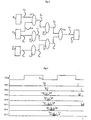
- Figure 4 shows an example of an elementary circuit inside a circuit integrated, to make a logical combination of signals from registers input 8, 9, 10, the result of which is available in a register 17.
- Nodes 11 to 16 are composed of transistors to obtain at the output of each node a binary signal resulting from input signals on this node.
- the node 11 receives as input a signal from the register 10.
- the node 12 receives an input signal from register 9.
- the node 13 receives as input a signal from register 8 and a signal from register 9.
- the node 14 receives as input a signal from the output of node 13.
- Node 15 receives as input a signal from the output of node 11 and a signal from the output of node 12.
- Node 16 receives as input a signal from the output of node 14 and a signal from the output of node 15.
- the output signal of node 16 is received at the entry of register 17.
- FIG. 5 is a chronogram plotting the time on the abscissa so as to represent for each element 11 to 17 of figure 4, the instants of crossing the switching threshold, as defined previously in reference to FIG. 3, at the input of one of these elements.
- the first line CLK represents the logic state of a clock whose, for example, the falling edge at an instant t f determines the emission of a binary signal at the output of the registers 8 to 10.
- the signal sent from register 10 is likely to cause switching at the input of node 11 at an instant t 11 .
- the delay t 11 - t f results from the coupling capacities of the conductor connecting the output of the register 10 to the input of the node 11 as explained previously with reference to FIGS. 2 and 3.
- the signal transmitted from register 9 is capable of causing switching at the input of node 12 at an instant t 12 .
- the delay t 12 - t f results from the coupling capacities of the conductor connecting the output of the register 9 to the input of the node 12 as explained previously with reference to FIGS. 2 and 3.
- the signal sent from register 8 is likely to cause switching at the input of node 13 at an instant t 13d .
- the delay t 13d - t f results from the coupling capacitances of the conductor connecting the output of the register 8 to the input of the node 13 as explained previously with reference to FIGS. 2 and 3.
- the signal emitted from the register 9 is likely to cause switching at the input of node 13 at an instant t 13f .
- the delay t 13f - t f results from the coupling capacities of the conductor connecting the output of the register 9 to the input of the node 13. Between the times t 13d and t 13f , the switching of the node 13 is indeterminate. This indeterminacy is symbolized by the small vertical hatching.
- the switching indeterminacy of node 13 refers to the input of node 14 from t 14d to t 14f .
- the delay t 14d - t 13d results from the coupling capacities of the conductor connecting the output of node 13 to the input of node 14 and from the intrinsic switching time of node 13.
- the signal transmitted from node 11 is likely to cause switching at the input of node 15 at an instant t 15d .
- the delay t 15d - t 11 results from the coupling capacities of the conductor connecting the output of node 11 to the input of node 15 and of the intrinsic switching time of node 11.
- the signal emitted from node 12 is likely to cause switching in entry of node 15 at time t 15f .
- the delay t 15f - t 12 results from the coupling capacities of the conductor connecting the output of node 12 to the input of node 15 and of the intrinsic switching time of node 12. Between times t 15d and t 15f , the switching of node 15 is undetermined. This indeterminacy is symbolized by the small vertical hatching.
- the switching indeterminacy of node 14 and the switching indeterminacy of node 15 refer to the input of node 16 from t 16d to t 16f .
- the delay t 16d - t 14d results from the coupling capacities of the conductor connecting the output of node 14 to the input of node 16 and from the intrinsic switching time of node 14.
- the delay t 16f - t 15f results from coupling capacities of the conductor connecting the output of node 15 to the input of node 16 and the intrinsic switching time of node 15.
- the switching indeterminacy of node 16 refers to the input of register 17 from t 17d to t 17f .
- the delay t 17d - t 17d results from the coupling capacities of the conductor connecting the output of node 16 to the input of register 17 and the intrinsic switching time of node 16.
- FIG. 6 presents a method for obtaining the switching instants of the elements of an electrical circuit.
- step E0 the physical parameters of the circuit are extracted, for example from the production masks which constitute a faithful image of the circuit produced from these masks. These physical parameters are inventoried in a connection list (netlist in English). Extraction from the masks is not necessary if we already have a list of connectors comprising for each electrical conductor L i of the circuit, the values of its resistance R i and of the actual existing capacities C ij of coupling with the other conductors. L j of which the mass at fixed potential Vss and the supply conductors at fixed potential Vdd are part.
- step E1 is generated for each conductor L i of the circuit, an equivalent capacitance value C Ti for coupling with respect to a mass of fixed potential.
- a device such as for example a computer, calculates a sum of the values of actual capacitances C ij existing for coupling of conductors L j of the circuit with the conductor L i .
- Each capacity C ij is assigned a weighting coefficient K ij .
- a step E2 follows on from step E1.
- a device such as for example the computer used in step E1, generates a switching time interval [t id , t if ] on each conductor L i .
- the generated switching time interval [t id , t if ] is stored in a data structure for further processing such as, for example, simply an output of results.
- the device calculates a time constant ⁇ i specific to the conductor L i , a function of the equivalent capacity C Ti generated in step E1.
- the switching instant t id is calculated as a function of the time constant ⁇ i and the instant of the first transmission at the output of the transmitter located upstream of the conductor.
- the switching instant t if is calculated as a function of the time constant ⁇ i and the instant of the last transmission at the output of the transmitter located upstream of the conductor. If these first and last transmission times are not already in the above-mentioned data structure, the device begins by generating them as a function of the switching times of the conductors located upstream of the transmitter considered, and so on, if necessary, until going back to the scales at the origin of the signal variations. Each original transmission is made at a time t f of the clock front.
- a step E3 precedes step E1 to generate these weighting coefficients.
- a device provided with digital processing means scans each conductor L i in the data structure at its disposal. The device then scans the data structure, each conductor L j having a real existing capacity C ij of coupling with the conductor L i considered. For each pair of conductors L i , L j , the device searches whether there is a switching time interval [t id , t if ] on the conductor L i and a switching time interval [t jd , t jf ] on the conductor L j with a common part.
- the device does not detect any information on the existence of a common part, it assigns a unit value to the weighting coefficient K ij . Indeed, no information then exists according to which the conductor L j behaves other than as a conductor with fixed potential during a switching on the conductor L i . This is always the case for conductors with fixed potential Vss or Vdd.
- the device If the device detects information on the existence of a common part, it searches whether the switching takes place on an identical value for the conductors L i and L j in this common part. It is for example possible that this second level of information is available when the conductors L i and L j convey the same signal.
- the device assigns to the coefficient K ij a value greater than the unit value. Indeed, no information then exists according to which a change in load of the conductor L j is not opposed to a change in load of the conductor L i . However, in a performance evaluation, it is preferable to consider the most unfavorable case. Taking into account the teaching given with reference to FIG. 3, a simple choice for the value of the coefficient K ij is a double value.
- the device assigns to the coefficient K ij a value lower than the unit value. Indeed, information then exists according to which a change in load of the conductor L j is not opposed to, or even contributes to a change in load of the conductor L i . However, in a performance evaluation, it is preferable to take into account a favorable case so as not to under-evaluate this performance. Taking into account the teaching given with reference to FIG. 3, a simple choice for the value of the coefficient K ij is a zero value.
- Step E3 is all the more efficient as the amount of information it has on the switching intervals, is consistent.
- Step E2 generates switching intervals which it is advantageous to use in step E3.
- a improvement of the process described consists in looping the output of step E2 back to the entry of step E3.
- a step E4 is interspersed between steps E2 and E3, of so as to be able to leave the loop thus constituted by steps E1 to E3.
- Step E4 constitutes an end test, which in the event of a break in the loop, leads to a step E5 for editing the switching intervals generated in step E2.
- Different tests can be considered in step E4.
- each of the conductors L i , L j , the indices i and j varying from 1 to the total number of conductors of the circuit, ten in the case described in FIG. 4, is listed in a data structure with its physical characteristics.
- step E3 When passing from step E0 to step E3, no switching interval is known a priori. In step E3, the weighting coefficients are therefore all initialized to a unit value.
- step E1 the coupling capacity of each conductor is then calculated by a first approximation which consists in supposing that, when a conductor considered L i commutes, no other neighboring conductor L j commutes.
- the total coupling capacity C Ti reduced to the substrate is equal to the sum of the real coupling capacity to the substrate C Si and the coupling capacities C ij of the conductor L i to the n conductors L j neighbors.
- VS Ti C Yes + ⁇ C ij (j ⁇ i, j ranging from 1 to n, n ⁇ 10)
- step E2 the instants and the switching intervals following a determined instant t f of the clock front, are calculated for each node of the analyzed circuit, on a model conforming to the explanations of FIG. 3, from the capacitance C Ti calculated in step E1. We thus obtain results similar to those of FIG. 5.
- Step E4 reconnects the process to step E3 where the coefficients of weightings are recalculated.
- steps E3 and E1 again generates a capacitance C Ti for each conductor joining two nodes using the results preceding from step E2. Take for example the case of Figure 5.
- FIG. 7 shows a use of the invention in a production method high integration fast circuits.
- An integrated circuit is commonly engraved in a semiconductor material from masks 55.
- Masks 55 therefore represent a true picture of the physical structure of the circuit.
- a phase extraction 56 allows to obtain from the masks, a list of connectors 57 which contains, in the form of a computer data structure, a list of all the conductors of the circuit and of the nodes which these conductors connect between them.
- the list also contains the physical characteristics of these drivers and of these nodes. These physical characteristics make it possible to determine by example, the resistance RL and the coupling capacities of each conductor, the switching threshold, immunity and transmit power of each node.
- a phase 58 of performance evaluation advantageously uses steps E1 to E5. If no time interval of switching edited in step E5 does not exceed one clock cycle, it is ensured that the circuit meets the performance objectives in terms of speed that we set our. In the case on the contrary, we use the results of step E5 to resize the circuit in phase 60.
- a phase 59 of immunity assessment consists of determine the node (s) of the circuits whose immunity is too low to resist crosstalk noises. Each of these nodes is associated with conductor brought upstream on his entry. If no knot does not contain knots unable to withstand crosstalk noises, we are assured that the circuit does not propagate crosstalk noises. Otherwise, we resize the circuit in one phase 60. Phase 58 can precede phase 59, so as to benefit from the instants of switching generated in step E2.
- a dimensioning phase 60 provides for the following corrective actions. For each offending component, conductor or node, one or more of the following actions are proposed.
- a first action consists in dimensioning the conductor so as to decrease its resistance. This has two advantages. The first advantage is that of decreasing its time constant. The second advantage is that of increasing its ability to supply a current to cancel parasitic charges caused by possible crosstalk noises.
- a second action consists in modifying the layout of the circuit so as to decrease the coupling capacities with other conductors of the circuit. This has two advantages. The first advantage is that of decreasing its time constant.
- a third action consists in dimensioning the receiver node connected downstream of the conductor so as to increase its immunity Im.
- a fourth action consists in dimensioning the transmitter node connected upstream of the conductor so as to increase its power.
- phase 60 a production phase 61 generates new masks 55 which incorporate any dimensioning carried out in phase 60. It is possible to repeat all or part of phases 56 to 61 on the new masks as well generated until phase 60 becomes unnecessary. The latest masks generated in phase 61 make it possible to create fast circuits with very high integration.
Landscapes
- Engineering & Computer Science (AREA)
- Computer Hardware Design (AREA)
- Physics & Mathematics (AREA)
- Theoretical Computer Science (AREA)
- Evolutionary Computation (AREA)
- Geometry (AREA)
- General Engineering & Computer Science (AREA)
- General Physics & Mathematics (AREA)
- Microelectronics & Electronic Packaging (AREA)
- Design And Manufacture Of Integrated Circuits (AREA)
- Testing Or Measuring Of Semiconductors Or The Like (AREA)
Claims (10)
- Verfahren zum Bewerten der Leistungsfähigkeit einer Schaltung mit sehr hoher Integration, mit einem ersten Schritt (E1), bei dem für jeden Leiter (L;) der Schaltung ein äquivalenter Kopplungskapazitätswert (CTi) in bezug auf eine Masse mit festem Potential als Summe von vorhandenen wirklichen Kopplungskapazitäten (Cij) von Leitern (Lj) der Schaltung mit diesem Leiter (Li) erzeugt wird, dadurch gekennzeichnet, daß die vorhandenen wirklichen Kapazitätswerte jeweils mit einem Gewichtungskoeffizienten (Kij) versehen werden und daß dem ersten Schritt ein zweiter Schritt (E2) folgt, bei dem ein Zeitintervall ([tid, tif]) der Aufschaltung auf jeden Leiter (Li) erzeugt wird, das zu einem ersten Zeitpunkt (tid) mit einer Verzögerung bezüglich eines Zeitpunkts des ersten Sendens beginnt und zu einem zweiten Zeitpunkt (tif) mit dieser Verzögerung bezüglich eines Zeitpunkts des zweiten Sendens auf dem Leiter (Li) endet, wobei die Verzögerung von der äquivalenten Kapazität (CTi) abhängt.
- Verfahren nach Anspruch 1, dadurch gekennzeichnet, daß es einen dritten Schritt (E3) umfaßt, der dem ersten Schritt (E1) vorhergeht und bei dem jeder der Koeffizienten (Kij) erzeugt wird als:ein Einheitswert bei Abwesenheit von Informationen, gemäß denen ein Zeitintervall ([tjd, tjf]) der Aufschaltung auf den Leiter (Lj), der eine vorhandene wirkliche Kopplungskapazität (Cij) mit dem Leiter (Li) hat, einen gemeinsamen Abschnitt mit dem Zeitintervall ([tid, tif]) der Aufschaltung auf den Leiter (Li) besitzt;ein Wert, der größer als der Einheitswert ist, wenn Informationen vorhanden sind, gemäß denen ein Zeitintervall ([tjd, tjf]) der Aufschaltung auf den Leiter (Lj), der eine vorhandene wirkliche Kopplungskapazität (Cij) mit dem Leiter (L;) hat, einen gemeinsamen Abschnitt mit dem Zeitintervall ([tid, tif]) der Aufschaltung auf den Leiter (Li) hat und wenn Informationen, gemäß denen das Schalten in dem gemeinsamen Abschnitt für die Leiter (Li) und (Lj) mit dem gleichen Wert erfolgt, nicht vorhanden sind;ein Wert, der kleiner als der Einheitswert ist, wenn Informationen vorhanden sind, gemäß denen ein Zeitintervall ([tjd, tjf]) der Aufschaltung auf den Leiter (Lj), der eine wirklich vorhandene Kopplungskapazität (Cij) mit dem Leiter (Li) besitzt, einen gemeinsamen Abschnitt mit dem Zeitintervall ([tid, tif]) der Aufschaltung auf den Leiter (Li) besitzt, und wenn Informationen vorhanden sind, gemäß denen das Schalten in dem gemeinsamen Abschnitt für die Leiter (Li) und (Lj) mit dem gleichen Wert erfolgt.
- Verfahren nach Anspruch 2, dadurch gekennzeichnet, daß der größere Wert gleich zwei ist und der kleinere Wert gleich null ist.
- Verfahren nach Anspruch 2 oder 3, dadurch gekennzeichnet, daß es einen vierten Schritt (E4) umfaßt, bei dem geprüft wird, ob das Verfahren beendet ist, und bei dem, wenn dies nicht der Fall ist, der Ausgang des zweiten Schrittes (E2) zum Eingang des dritten Schrittes (E3) zurückgeschleift wird.
- Vorrichtung zum Bewerten der Leistungsfähigkeit einer Schaltung mit sehr hoher Integration, mit ersten Mitteln, die für jeden Leiter (Li) der Schaltung einen äquivalenten Kopplungskapazitätswert (CTi) in bezug auf eine Masse mit festem Potential als eine Summe von vorhandenen wirklichen Kopplungskapazitätswerten von Leitern (Lj) der Schaltung mit diesem Leiter (Li) berechnen, dadurch gekennzeichnet, daß die vorhandenen wirklichen Kapazitätswerte jeweils mit einem Gewichtungskoeffizienten (Kij) versehen sind und daß die Vorrichtung außerdem zweite Mittel umfaßt, die ein Zeitintervall ([tid, tif]) der Aufschaltung auf den Leiter (Li) berechnen, das zu einem ersten Zeitpunkt (tid) mit einer Verzögerung bezüglich eines Zeitpunkts des ersten Sendens beginnt und zu einem zweiten Zeitpunkt (tif) mit dieser Verzögerung bezüglich eines Zeitpunkts des zweiten Sendens auf dem Leiter (L;) endet, wobei die Verzögerung von der äquivalenten Kapazität (CTi) abhängt.
- Vorrichtung nach Anspruch 5, dadurch gekennzeichnet, daß sie dritte Mittel umfaßt, die jeden der Koeffizienten (Kij) berechnen alseinen Einheitswert, falls die Vorrichtung keine Informationen liefert, gemäß denen ein Zeitintervall ([tjd, tjf]) der Aufschaltung auf den Leiter (Lj), der eine vorhandene wirkliche Kopplungskapazität (Cij) mit dem Leiter (L;) hat, einen gemeinsamen Abschnitt mit dem Zeitintervall ([tid, tif]) der Aufschaltung auf den Leiter (L;) besitzt;einen Wert, der größer als der Einheitswert ist, falls die Vorrichtung Informationen liefert, gemäß denen ein Zeitintervall ([tjd, tjf]) der Aufschaltung auf den Leiter (Lj), der eine vorhandene wirkliche Kopplungskapazität (Cij) mit dem Leiter (L;) hat, einen gemeinsamen Abschnitt mit dem Zeitintervall ([tid, tif]) der Aufschaltung auf den Leiter (L;) besitzt, und falls die Vorrichtung keine Informationen liefert, gemäß denen das Schalten in dem gemeinsamen Abschnitt für die Leiter (Li) und (Lj) mit demselben Wert erfolgt;einen Wert, der kleiner als der Einheitswert ist, falls die Vorrichtung Informationen bereitstellt, gemäß denen ein Zeitintervall ([tjd, tjf]) der Aufschaltung auf den Leiter (Lj), der eine vorhandene wirkliche Kopplungskapazität (Cij) mit dem Leiter (L;) hat, einen gemeinsamen Abschnitt mit dem Zeitintervall ([tid, tif]) der Aufschaltung auf den Leiter (L;) besitzt, und falls die Vorrichtung Informationen bereitstellt, gemäß denen das Schalten in dem gemeinsamen Abschnitt für die Leiter (L;) und Lj) mit demselben Wert erfolgt.
- Vorrichtung nach Anspruch 6, dadurch gekennzeichnet, daß der größere Wert gleich zwei ist und der kleinere Wert gleich null ist.
- Vorrichtung nach Anspruch 6 oder 7, dadurch gekennzeichnet, daß sie vierte Mittel umfaßt, die prüfen, ob die von den zweiten Mitteln erzeugten Informationen zu den ersten Mitteln zurückgeschleift werden sollen oder nicht.
- Verfahren für die Verwirklichung einer elektrischen Schaltung, das eine Phase (61) für die Produktion von Masken (55) enthält und dadurch gekennzeichnet ist, daß es umfaßt:eine Phase (58) der Bewertung von Maskenbestandteilen, in der das Verfahren nach einem der Ansprüche 1 bis 4 ausgeführt wird;eine Dimensionierungsphase (60), in der alle oder einige der Bestandteile, die in der Bewertungsphase (58) beanstandet wurden, dimensioniert werden; undeine Wiederholung der Phase (61) mit den in der Phase (60) dimensionierten Bestandteilen.
- Computerprogramm, das Programmcode-Abschnitte/-Mittel/-Befehle für die Ausführung der Schritte des Verfahrens nach einem der Ansprüche 1 bis 4 und 9, wenn das Programm auf einem Computer ausgeführt wird, umfaßt.
Priority Applications (5)
| Application Number | Priority Date | Filing Date | Title |
|---|---|---|---|
| DE69811469T DE69811469T2 (de) | 1998-01-22 | 1998-01-22 | Verfahren zur Leistungsbewertung von VLSI-Schaltungen |
| EP01109830A EP1128292A1 (de) | 1998-01-22 | 1998-01-22 | Verfahren zur Abschätzung der Eignung einer Vlsi-Schaltung zum Widerstehen von Übersprechraushen |
| EP98400134A EP0932110B1 (de) | 1998-01-22 | 1998-01-22 | Verfahren zur Leistungsbewertung von VLSI-Schaltungen |
| US09/233,939 US6370674B1 (en) | 1998-01-22 | 1999-01-20 | Process for evaluating the performance of very high scale integrated circuits |
| JP01286699A JP3244226B2 (ja) | 1998-01-22 | 1999-01-21 | 超大規模集積回路の性能を評価する方法 |
Applications Claiming Priority (1)
| Application Number | Priority Date | Filing Date | Title |
|---|---|---|---|
| EP98400134A EP0932110B1 (de) | 1998-01-22 | 1998-01-22 | Verfahren zur Leistungsbewertung von VLSI-Schaltungen |
Related Child Applications (1)
| Application Number | Title | Priority Date | Filing Date |
|---|---|---|---|
| EP01109830A Division EP1128292A1 (de) | 1998-01-22 | 1998-01-22 | Verfahren zur Abschätzung der Eignung einer Vlsi-Schaltung zum Widerstehen von Übersprechraushen |
Publications (2)
| Publication Number | Publication Date |
|---|---|
| EP0932110A1 EP0932110A1 (de) | 1999-07-28 |
| EP0932110B1 true EP0932110B1 (de) | 2003-02-19 |
Family
ID=8235246
Family Applications (2)
| Application Number | Title | Priority Date | Filing Date |
|---|---|---|---|
| EP98400134A Expired - Lifetime EP0932110B1 (de) | 1998-01-22 | 1998-01-22 | Verfahren zur Leistungsbewertung von VLSI-Schaltungen |
| EP01109830A Withdrawn EP1128292A1 (de) | 1998-01-22 | 1998-01-22 | Verfahren zur Abschätzung der Eignung einer Vlsi-Schaltung zum Widerstehen von Übersprechraushen |
Family Applications After (1)
| Application Number | Title | Priority Date | Filing Date |
|---|---|---|---|
| EP01109830A Withdrawn EP1128292A1 (de) | 1998-01-22 | 1998-01-22 | Verfahren zur Abschätzung der Eignung einer Vlsi-Schaltung zum Widerstehen von Übersprechraushen |
Country Status (4)
| Country | Link |
|---|---|
| US (1) | US6370674B1 (de) |
| EP (2) | EP0932110B1 (de) |
| JP (1) | JP3244226B2 (de) |
| DE (1) | DE69811469T2 (de) |
Families Citing this family (7)
| Publication number | Priority date | Publication date | Assignee | Title |
|---|---|---|---|---|
| US6536022B1 (en) * | 2000-02-25 | 2003-03-18 | Sun Microsystems, Inc. | Two pole coupling noise analysis model for submicron integrated circuit design verification |
| US6507935B1 (en) * | 2000-02-25 | 2003-01-14 | Sun Microsystems, Inc. | Method of analyzing crosstalk in a digital logic integrated circuit |
| JP4232477B2 (ja) * | 2003-02-13 | 2009-03-04 | パナソニック株式会社 | 半導体集積回路の検証方法 |
| US7093211B1 (en) * | 2003-11-03 | 2006-08-15 | General Electric Company | Techniques for modeling current spreading uniformity in light emitting diodes |
| US8095903B2 (en) * | 2004-06-01 | 2012-01-10 | Pulsic Limited | Automatically routing nets with variable spacing |
| EP1662410A1 (de) * | 2004-11-30 | 2006-05-31 | Infineon Technologies AG | Verfahren und Vorrichtung zum Analysieren der Nebensprecheffekten in einem elektronischen Gerät |
| US7549136B2 (en) * | 2006-01-11 | 2009-06-16 | Virage Logic Corp. | System and method for approximating intrinsic capacitance of an IC block |
Family Cites Families (10)
| Publication number | Priority date | Publication date | Assignee | Title |
|---|---|---|---|---|
| US4587620A (en) * | 1981-05-09 | 1986-05-06 | Nippon Gakki Seizo Kabushiki Kaisha | Noise elimination device |
| US5127021A (en) * | 1991-07-12 | 1992-06-30 | Schreiber William F | Spread spectrum television transmission |
| US5687088A (en) * | 1993-05-19 | 1997-11-11 | Matsushita Electric Industrial Co., Ltd. | Net list for use in logic simulation and back annotation method of feedbacking delay information obtained through layout design to logic simulation |
| US5481695A (en) * | 1993-10-26 | 1996-01-02 | Cadence Design Systems, Inc. | System and method for estimating crosstalk between signal lines in a circuit |
| US5502644A (en) * | 1994-04-07 | 1996-03-26 | At&T Corp. | Process and apparatus for auditing crosstalk and characteristic impedances of printed wiring boards |
| US5568395A (en) * | 1994-06-29 | 1996-10-22 | Lsi Logic Corporation | Modeling and estimating crosstalk noise and detecting false logic |
| US5555506A (en) * | 1995-02-09 | 1996-09-10 | Unisys Corporation | Method of fabricating IC chips with equation estimated statistical crosstalk voltages being less than noise margin |
| US5910730A (en) * | 1996-12-13 | 1999-06-08 | International Business Machines Corporation | Digital circuit noise margin improvement |
| FR2767982B1 (fr) * | 1997-09-04 | 2001-11-23 | Sgs Thomson Microelectronics | Circuit a retard variable |
| JP3005578B1 (ja) | 1999-03-01 | 2000-01-31 | 日本電気アイシーマイコンシステム株式会社 | クロスト―ク検証装置およびクロスト―ク検証方法 |
-
1998
- 1998-01-22 EP EP98400134A patent/EP0932110B1/de not_active Expired - Lifetime
- 1998-01-22 EP EP01109830A patent/EP1128292A1/de not_active Withdrawn
- 1998-01-22 DE DE69811469T patent/DE69811469T2/de not_active Expired - Lifetime
-
1999
- 1999-01-20 US US09/233,939 patent/US6370674B1/en not_active Expired - Lifetime
- 1999-01-21 JP JP01286699A patent/JP3244226B2/ja not_active Expired - Fee Related
Also Published As
| Publication number | Publication date |
|---|---|
| JP2000068384A (ja) | 2000-03-03 |
| JP3244226B2 (ja) | 2002-01-07 |
| EP0932110A1 (de) | 1999-07-28 |
| DE69811469T2 (de) | 2003-11-27 |
| DE69811469D1 (de) | 2003-03-27 |
| US6370674B1 (en) | 2002-04-09 |
| EP1128292A1 (de) | 2001-08-29 |
Similar Documents
| Publication | Publication Date | Title |
|---|---|---|
| EP0198729B1 (de) | System zur Simulation einer elektronischen Schaltung | |
| FR2786961A1 (fr) | Dispositif electronique pour systeme de cablage de bus | |
| FR2822263A1 (fr) | Systeme et procede de determination de la sensibilite au bruit d'un circuit integre | |
| FR2682521A1 (fr) | Dispositif integre a memoire a semiconducteurs. | |
| FR2544143A1 (fr) | Reseau logique programme comportant des moyens auxiliaires de connexion au potentiel positif pour augmenter la vitesse de precharge | |
| FR2466906A1 (fr) | Circuit detecteur de transitions d'un niveau de signal a un autre | |
| EP0020999B1 (de) | Prüfer und Verfahren zur Messung der Speicheradressenzugriffszeit mittels einer Datenwiederumlauftechnik | |
| FR2619939A1 (fr) | Circuit de detection de transitions d'adresses | |
| EP1128292A1 (de) | Verfahren zur Abschätzung der Eignung einer Vlsi-Schaltung zum Widerstehen von Übersprechraushen | |
| EP0971297A1 (de) | Verfahren zur Anordnung der Leitungsführung einer zentralen Taktgeberschaltung auf einem integrierten Schaltkreis sowie zugehörigen Vorrichtungen | |
| EP0206892A1 (de) | Verarbeitungsverfahren für ein ursprüngliches Bild darstellende digitale Signale | |
| WO2008007026A2 (fr) | Procédé de modélisation de l'activité de commutation d'un circuit numérique | |
| EP0463964B2 (de) | Anlage zur Erzeugung und zum Empfang von Ultraschall | |
| FR2679672A1 (fr) | Circuit de transmission de donnees avec des lignes d'entree/sortie segmentees. | |
| BE898544R (fr) | Calculateur associatif permettant une multiplication rapide. | |
| FR2499788A1 (fr) | Circuit generateur d'impulsions utilisant une source de courant et ensemble de memorisation utilisant un tel circuit | |
| WO2008001010A2 (fr) | Procédé de modélisation du bruit injecté dans un système électronique | |
| EP0229433B1 (de) | Vorrichtung zum Prüfen eines kombinatorischen logischen Schaltkreises | |
| FR2690026A1 (fr) | Dispositif de mémoire destiné à supprimer le bruit produit entre des lignes de signaux. | |
| EP0140413B1 (de) | Dekodierschaltung für statischen RAM-Speicher | |
| EP0899921B1 (de) | Symmetrischer Leitungstreiber | |
| FR2604577A1 (fr) | Circuit generateur de code a bruit pseudo-aleatoire | |
| EP1292840B1 (de) | Verfahren zum nachweisen der abhängigkeit eines signals von einem anderen signal | |
| FR2682801A1 (fr) | Circuit pour produire une tension d'alimentation en courant interne dans un dispositif de memoire a semiconducteurs. | |
| FR2805686A1 (fr) | Dispositif pour eliminer les effets des reflexions entre un circuit de commande et plusieurs recepteurs |
Legal Events
| Date | Code | Title | Description |
|---|---|---|---|
| PUAI | Public reference made under article 153(3) epc to a published international application that has entered the european phase |
Free format text: ORIGINAL CODE: 0009012 |
|
| AK | Designated contracting states |
Kind code of ref document: A1 Designated state(s): DE FR GB IT |
|
| AX | Request for extension of the european patent |
Free format text: AL;LT;LV;MK;RO;SI |
|
| 17P | Request for examination filed |
Effective date: 20000128 |
|
| AKX | Designation fees paid |
Free format text: DE FR GB IT |
|
| 17Q | First examination report despatched |
Effective date: 20000529 |
|
| GRAH | Despatch of communication of intention to grant a patent |
Free format text: ORIGINAL CODE: EPIDOS IGRA |
|
| RTI1 | Title (correction) |
Free format text: METHOD FOR EVALUATING THE PERFORMANCE OF VLSI CIRCUITS |
|
| RTI1 | Title (correction) |
Free format text: METHOD FOR EVALUATING THE PERFORMANCE OF VLSI CIRCUITS |
|
| GRAH | Despatch of communication of intention to grant a patent |
Free format text: ORIGINAL CODE: EPIDOS IGRA |
|
| GRAA | (expected) grant |
Free format text: ORIGINAL CODE: 0009210 |
|
| AK | Designated contracting states |
Designated state(s): DE FR GB IT |
|
| REG | Reference to a national code |
Ref country code: GB Ref legal event code: FG4D Free format text: NOT ENGLISH |
|
| GBT | Gb: translation of ep patent filed (gb section 77(6)(a)/1977) |
Effective date: 20030219 |
|
| REF | Corresponds to: |
Ref document number: 69811469 Country of ref document: DE Date of ref document: 20030327 Kind code of ref document: P |
|
| PLBE | No opposition filed within time limit |
Free format text: ORIGINAL CODE: 0009261 |
|
| STAA | Information on the status of an ep patent application or granted ep patent |
Free format text: STATUS: NO OPPOSITION FILED WITHIN TIME LIMIT |
|
| 26N | No opposition filed |
Effective date: 20031120 |
|
| REG | Reference to a national code |
Ref country code: FR Ref legal event code: PLFP Year of fee payment: 19 |
|
| PGFP | Annual fee paid to national office [announced via postgrant information from national office to epo] |
Ref country code: GB Payment date: 20151224 Year of fee payment: 19 |
|
| PGFP | Annual fee paid to national office [announced via postgrant information from national office to epo] |
Ref country code: FR Payment date: 20151222 Year of fee payment: 19 |
|
| PGFP | Annual fee paid to national office [announced via postgrant information from national office to epo] |
Ref country code: DE Payment date: 20151217 Year of fee payment: 19 Ref country code: IT Payment date: 20160111 Year of fee payment: 19 |
|
| REG | Reference to a national code |
Ref country code: DE Ref legal event code: R119 Ref document number: 69811469 Country of ref document: DE |
|
| GBPC | Gb: european patent ceased through non-payment of renewal fee |
Effective date: 20170122 |
|
| REG | Reference to a national code |
Ref country code: FR Ref legal event code: ST Effective date: 20170929 |
|
| PG25 | Lapsed in a contracting state [announced via postgrant information from national office to epo] |
Ref country code: FR Free format text: LAPSE BECAUSE OF NON-PAYMENT OF DUE FEES Effective date: 20170131 |
|
| PG25 | Lapsed in a contracting state [announced via postgrant information from national office to epo] |
Ref country code: GB Free format text: LAPSE BECAUSE OF NON-PAYMENT OF DUE FEES Effective date: 20170122 Ref country code: DE Free format text: LAPSE BECAUSE OF NON-PAYMENT OF DUE FEES Effective date: 20170801 |
|
| PG25 | Lapsed in a contracting state [announced via postgrant information from national office to epo] |
Ref country code: IT Free format text: LAPSE BECAUSE OF NON-PAYMENT OF DUE FEES Effective date: 20170122 |