EP0921626B1 - Switching-type DC power source apparatus - Google Patents
Switching-type DC power source apparatus Download PDFInfo
- Publication number
- EP0921626B1 EP0921626B1 EP98122937A EP98122937A EP0921626B1 EP 0921626 B1 EP0921626 B1 EP 0921626B1 EP 98122937 A EP98122937 A EP 98122937A EP 98122937 A EP98122937 A EP 98122937A EP 0921626 B1 EP0921626 B1 EP 0921626B1
- Authority
- EP
- European Patent Office
- Prior art keywords
- current
- voltage
- circuit
- output
- power source
- Prior art date
- Legal status (The legal status is an assumption and is not a legal conclusion. Google has not performed a legal analysis and makes no representation as to the accuracy of the status listed.)
- Expired - Lifetime
Links
- 238000001514 detection method Methods 0.000 claims description 25
- 239000003990 capacitor Substances 0.000 description 9
- 238000009499 grossing Methods 0.000 description 9
- 230000007423 decrease Effects 0.000 description 4
- 238000010586 diagram Methods 0.000 description 4
- 238000003079 width control Methods 0.000 description 4
- 230000000694 effects Effects 0.000 description 2
- 238000000034 method Methods 0.000 description 2
- 241000826860 Trapezium Species 0.000 description 1
- 230000001419 dependent effect Effects 0.000 description 1
- 238000011161 development Methods 0.000 description 1
- 230000018109 developmental process Effects 0.000 description 1
- 238000007599 discharging Methods 0.000 description 1
- 230000005669 field effect Effects 0.000 description 1
- 238000012986 modification Methods 0.000 description 1
- 230000004048 modification Effects 0.000 description 1
Images

Classifications
-
- H—ELECTRICITY
- H02—GENERATION; CONVERSION OR DISTRIBUTION OF ELECTRIC POWER
- H02M—APPARATUS FOR CONVERSION BETWEEN AC AND AC, BETWEEN AC AND DC, OR BETWEEN DC AND DC, AND FOR USE WITH MAINS OR SIMILAR POWER SUPPLY SYSTEMS; CONVERSION OF DC OR AC INPUT POWER INTO SURGE OUTPUT POWER; CONTROL OR REGULATION THEREOF
- H02M1/00—Details of apparatus for conversion
- H02M1/42—Circuits or arrangements for compensating for or adjusting power factor in converters or inverters
- H02M1/4208—Arrangements for improving power factor of AC input
- H02M1/4225—Arrangements for improving power factor of AC input using a non-isolated boost converter
-
- Y—GENERAL TAGGING OF NEW TECHNOLOGICAL DEVELOPMENTS; GENERAL TAGGING OF CROSS-SECTIONAL TECHNOLOGIES SPANNING OVER SEVERAL SECTIONS OF THE IPC; TECHNICAL SUBJECTS COVERED BY FORMER USPC CROSS-REFERENCE ART COLLECTIONS [XRACs] AND DIGESTS
- Y02—TECHNOLOGIES OR APPLICATIONS FOR MITIGATION OR ADAPTATION AGAINST CLIMATE CHANGE
- Y02B—CLIMATE CHANGE MITIGATION TECHNOLOGIES RELATED TO BUILDINGS, e.g. HOUSING, HOUSE APPLIANCES OR RELATED END-USER APPLICATIONS
- Y02B70/00—Technologies for an efficient end-user side electric power management and consumption
- Y02B70/10—Technologies improving the efficiency by using switched-mode power supplies [SMPS], i.e. efficient power electronics conversion e.g. power factor correction or reduction of losses in power supplies or efficient standby modes
Definitions
- the present invention relates to a switching-type DC (direct current) power source in which an active filter is used.
- a capacitor-input rectifier circuit has been widely applied as a rectifier smoothing circuit to a switching-type DC power source apparatus.
- an input current flows only in a discharging period, i.e., an "ON" period of a smoothing capacitor. Therefore, in a practical state, a pulse-like input current having a peak value several times as much as an effective value of the input current tends to flow in this circuit, and also a power factor is restrained to 0.6 or so. For this reason, a harmonic noise occurred due to such the low power factor has become problem.
- a pulse-like current waveform includes a number of harmonic components
- plural equipments each of which has the power source apparatus applying the capacitor-input rectifier circuit are connected to an identical commercial AC (alternate current) power source line
- a commercial AC line waveform is distorted as the number of connected equipments increases, whereby an operation of one equipment may cause erroneous operations of the other equipments.
- a peak current and a line impedance due to a peak current and a line impedance, a top of a commercial AC voltage waveform is crushed and thus the waveform becomes a trapezoid or trapezium.
- Even in such a state since it generally continues to supply constant power, a commercial AC current further increases, whereby a pulse waveform becomes still more sharp. Thus, such a phenomenon further increases voltage drop, resulting in vicious circle.
- an active filter capable of increasing a filter effect by switching active elements such as a transistor, an FET (field effect transistor) and the like at high speed and also capable of downsizing the power source apparatus has been come into notice.
- a switching power source apparatus using the active filter in its rectifier unit has various advantages. That is, the apparatus has a switching power source function to always maintain an output voltage at a constant level even if an input voltage varies.
- the apparatus detects the commercial AC input current and the commercial AC input voltage waveform and performs pulse-width control (PWM control) such that a commercial AC input current waveform becomes analogous to the commercial AC input voltage waveform.
- PWM control pulse-width control
- the input current always has a sine wave, whereby it becomes possible to increase the power factor and reduce the harmonic noise.
- a current to be input to the smoothing capacitor can be suppressed to 1/10 to 1/5 as compared with the conventional capacitor-input rectifier circuit.
- capacity of the smoothing capacitor can be made smaller, whereby the entire apparatus can be made compact in size.
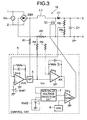
- Fig. 3 is a diagram showing a structure of a conventional switching-type DC power source apparatus.
- This power source apparatus uses a booster-chopper type active filter, and an input side thereof is connected to AC power source input terminals 1 and 2. Further, this power source apparatus is composed of a rectifier circuit (e.g., diode bridge) DB1 which performs full-wave rectification of an AC input power source voltage, and a booster-chopper type active filter circuit (to be referred simply as active filter hereinafter) 10 which performs smoothing on a pulsating voltage output from the diode bridge DB1 and outputs a DC voltage.
- DC-DC converters are respectively connected to output terminals 3 and 4 of the active filter 10 as loads, and DC constant voltage of 5V, 24V or the like is supplied to the respective loads.
- the active filter 10 is composed of a choke coil L1 which is connected to a plus(+)-side output terminal of the diode bridge DB1, a switching element (e.g., FET) Q1 which performs switching of the pulsating voltage full-wave rectified by the diode bridge DB1, a rectifier diode D1 which transfers electromagnetic energy stored in the choke coil L1 and prevents counter flowing of energy stored in a smoothing capacitor C1 to rectify the pulsating voltage, a sine wave detection resistor R1 which detects an input voltage (i.e., pulsating voltage) waveform rectified by the diode bridge DB1, a current detection resistor R2 which detects a current flowing in the circuit 10, output voltage detection resistors R5 and R6 which detect the output voltage, the smoothing capacitor C1, an active filter control circuit (to be referred simply as control circuit hereinafter) 5 which performs pulse-width modulation (PWM) control on a drive pulse (i.e., gate pulse) to drive the
- the control circuit 5 is composed of a voltage error amplifier VEA which performs output constant voltage control, a current error amplifier IEA which controls a commercial input current waveform to be a sine wave, a multiplier (MP) 6 which gives a predetermined threshold to the current error amplifier IEA, an oscillator (OSC) 8, a maximum ON duty restriction voltage source Vref2 which restricts maximum ON duty of the drive pulse, a minimum value voltage selection circuit 7 which selects lower one of outputs of the amplifier IEA and the voltage source Vref2 and then supplies the selected output to a comparator COMP, the comparator COMP which compares an output waveform of the circuit 7 and an output waveform of the oscillator 8 with each other and then outputs a drive pulse to turn on and off the switching FET Q1, and the like.
- the commercial AC voltage supplied from the input terminals 1 and 2 is full-wave rectified by the diode bridge DB1, and the obtained pulsating voltage is then supplied to the active filter 10.
- the filter 10 performs switching on the supplied pulsating voltage by using the switching FET Q1 at a frequency equal to or higher than several tens kHz during an entire period.
- the current flows in the FET Q1 through the choke coil L1, whereby the electromagnetic energy is stored in the coil L1.
- the electromagnetic energy stored in the coil L1 charges the smoothing capacitor C1 through the rectifier diode D1 and is also supplied to the load such as the DC-DC converter or the like through the output terminal 3.
- ON and OFF of the switching FET Q1 are controlled by the control circuit 5 to output the DC constant voltage to the output terminals 3 and 4. Also, the PWM control is performed by the circuit 5 such that the input current waveform becomes the sine wave.
- the control circuit 5 detects the output voltage by using the output voltage detection resistors R5 and R6, detects the full-wave rectified pulsating voltage waveform by using the sine wave detection resistor R1, detects the current flowing in the circuit 10 by using the current detection resistor R2, outputs the DC constant voltage to the output terminals 3 and 4, and controls a width of the drive pulse (i.e., gate pulse) to be supplied to a gate of the FET Q1 being the switching element such that the AC input current flowing in the circuit comes to have the sine waveform.
- Vcc denotes a power source voltage of the control circuit 5.
- the voltage error amplifier VEA In order to stabilize the output DC voltage against load variation and input variation, the voltage error amplifier VEA outputs a DC voltage (this voltage determines magnitude of threshold being output of multiplier 6) such that a divided voltage value of the output voltage detected by the resistors (i.e., output voltage division resistors) R5 and R6 becomes equal to a reference voltage Vref1.
- the multiplier 6 multiplies the sine waveform (this waveform determines output waveform of multiplier 6) detected by the sine wave detection resistor R1 and the output of the voltage error amplifier VEA together, and then outputs a voltage being a threshold of the current error amplifier IEA.
- the current error amplifier IEA operates such that, in the circuit, the current corresponding to voltage drop at the current detection resistor R2 becomes equal to the threshold voltage being the output of the multiplier 6.
- the comparator COMP compares the output of the amplifier IEA and the output of the oscillator 8 with each other to obtain the pulse for driving the switching FET Q1.
- ON duty is controllable within a range from 0% to 100% in principle.
- the FET Q1 practically operates at ON duty 100% or so when an instantaneous value of the commercial AC power source being an input is close to "0" volt.
- the maximum ON duty restriction voltage source Vref2 (voltage therefrom is determined based on amplitude of oscillator 8 and setting maximum ON duty) and the minimum value voltage selection circuit 7 are provided.
- the output of the amplifier IEA and the output of the source Vref2 are compared with each other, and lower-voltage one is then input to the comparator COMP. That is, if the source Vref2 is set to have the voltage of ON duty 80% or so, the ON duty does not exceed 80% even if the amplifier IEA requires the ON duty 100% or so.
- Figs. 4A to 4C are views showing examples of waveforms at respective units in Fig. 3 .
- Fig. 4A shows the waveform of an output voltage VIEAout of the current error amplifier IEA
- Fig. 4B shows the waveform of an AC input current Iin
- Fig. 4C shows the waveform of an AC input voltage Vin.
- the ordinary PWM control i.e., pulse width control
- an instantaneous value of the voltage Vin gradually decreases, and an operation at the maximum ON duty starts at the time t2.
- an output voltage VIEAout acts to expand an ON time width of the drive pulse and such a state is fixed.
- the AC input voltage Vin once becomes "0" volt, and the instantaneous value gradually increases.
- the voltage VIEAout then acts to narrow the drive pulse.
- the voltage VIEAout slowly decreases, whereby it takes a long time until the voltage VIEAout in the above fixed state changes to have an ON time width desired by the multiplier 6. That is, the change of the voltage VIEAout overtakes at a time t4.
- EP-A-0 744 816 discloses switching-type DC power source apparatus according to the preamble of claim 1, comprising an AC to DC rectifier for inputting an AC current and outputting a rectified DC current, a boost power train for boosting the output DC current, a current detection circuit for detecting the output current of the boost power train, a pulse-width modulator for controlling the boost power train via a MOS-FET, and an output voltage control loop for supplying a current to the current amplifier also at zero level.
- EP-A-0 573 828 discloses a power supply unit comprising a rectifier mean, an inductor, a power switch, an output rectifier, an output filter capacitor and a control circuit, wherein said control circuit consists of an error amplifier, a multiplier and a pulse modulator arranged in parallel.
- the error amplifier receives a constant reference voltage and compares it with the voltage at the output of the filter capacitor of the power supply, thereby generating an error signal that is sent to a multiplier, which is also supplied with the rectified input voltage from the input rectifier, so that said multiplier performs a multiplication of said signals and generates in turn a multiplication signal that is applied to a purse modulator that issues corresponding control pulses for the power switch.
- the input current desired as the multiplier output does not flow in the period during which the maximum ON duty is restricted, i.e., when the instantaneous value of the commercial AC power source being the input is close to "0" volt. Therefore, there is a case where the output of the current error amplifier continues to act to expand or widen the pulse width.
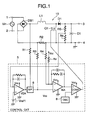
- Fig. 1 is a diagram showing a structure of a switching-type DC power source apparatus according to the present invention.
- Fig. 1 since the parts denoted by the same reference numerals and symbols as those in Fig. 3 are the same as the parts mentioned in the related background art, explanation thereof is omitted in the embodiment.
- the switching-type DC power source apparatus shown Fig. 1 is different from that shown in Fig. 3 in the point that a resistor Rv is connected between a power source Vcc of a control circuit 5 and an inversion input terminal of a current error amplifier IEA, and in the point that the minimum value voltage selection circuit 7 and the maximum ON duty restriction voltage source Vref2 both shown in Fig. 3 are omitted.
- a commercial AC voltage supplied from input terminals 1 and 2 is full-wave rectified by a diode bridge DB1, and an obtained pulsating voltage is then supplied to an active filter 10.
- the filter 10 performs switching on the supplied pulsating voltage by using a switching FET Q1 at a frequency equal to or higher than several tens kHz during an entire period. In a period during which the FET Q1 is ON, the current flows in the FET Q1 through a choke coil L1, whereby an electromagnetic energy is stored in the coil L1.
- the electromagnetic energy stored in the coil L1 charges a smoothing capacitor C1 through a rectifier diode D1 and is also supplied to a load such as a DC-DC converter or the like through an output terminal 3.
- ON and OFF of the switching FET Q1 are controlled by the control circuit 5 to output a DC constant voltage to the output terminals 3 and 4. Also, PWM control (i.e., pulse width control) is performed by the circuit 5 such that an input current waveform becomes a sine wave.
- PWM control i.e., pulse width control
- the control circuit 5 detects the output voltage by using output voltage detection resistors R5 and R6, detects a full-wave rectified pulsating voltage waveform by using a sine wave detection resistor R1, detects a current flowing in the circuit 10 by using a current detection resistor R2, outputs the DC constant voltage to the output terminals 3 and 4, and also controls a width of a drive pulse (i.e., gate pulse) to be supplied to a gate of the FET Q1 being a switching element such that the AC input current flowing in the circuit comes to have the sine waveform.
- a drive pulse i.e., gate pulse
- an voltage error amplifier VEA In order to stabilize the output DC voltage against load variation and input variation, an voltage error amplifier VEA outputs a DC voltage (this voltage determines magnitude of threshold being output of multiplier 6) such that a divided voltage value of the output voltage detected by the output voltage division resistors R5 and R6 becomes equal to a reference voltage Vref1.
- the multiplier 6 multiplies the sine waveform (this waveform determines output waveform of multiplier 6) detected by the sine wave detection resistor R1 and the output of the voltage error amplifier VEA together, and then outputs a threshold voltage for the current error amplifier IEA.
- the current error amplifier IEA operates such that, in the circuit, the current corresponding to voltage drop at the current detection resistor R2 becomes equal to the threshold voltage being the output of the multiplier 6.
- the comparator COMP compares an output of the amplifier IEA and an output of the oscillator (OSC) 8 with each other to generate a pulse for driving the switching FET Q1.
- ON duty is controllable within a range from 0% to 100% in principle.
- the FET Q1 practically operates at ON duty 100% or so when an instantaneous value of a commercial AC power source being an input is close to "0" volt.
- the resistor Rv acting as a current supply means is added, from a viewpoint of the current error amplifier IEA, the current seems to be flowing in the current detection resistor R2. That is, the current is seemingly flowing in the resistor R2.
- the output of the current error amplifier IEA acts to narrow a pulse width when the instantaneous value falls below a certain value.
- the output of the amplifier IEA acts to gradually expand or widen the pulse width when the instantaneous value exceeds the certain value. For this reason, the FET Q1 operates such that it softly starts at each cycle of commercial AC frequency, thereby preventing a prickle-like current from flowing.
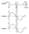
- Figs. 2A to 2C are views showing examples of waveforms at respective units in Fig. 1 .
- Fig. 2A shows the waveform of an output voltage VIEAout of the current error amplifier IEA
- Fig. 2B shows the waveform of an AC input current Iin
- Fig. 2C shows the waveform of an AC input voltage Vin.
- Figs. 2A to 2C during a period from a time t1 to a time t2, the ordinary PWM control (i.e., pulse width control) is performed. Then, the instantaneous value of the AC input voltage Vin gradually decreases, relation on magnitude between the seeming current based on the voltage Vcc and the resistor R2 and the input current Iin is inverted at the time t2, and the current error amplifier IEA starts operating to narrow the ON time width of the drive pulse.
- the ordinary PWM control i.e., pulse width control
- the current error amplifier IEA starts operating to again expand the drive pulse at a time t3 and gradually expands the ON time width of the drive pulse up to a time t4.
- the expanded width coincides with the pulse width required by the multiplier 6.
- the FET Q1 causes the FET Q1 to softly start operating.
- the state at the time t4 is identical with that at the time t1.
- the added resistor Rv makes the certain amount of current as if it is always flowing in the current detection resistor R2 (i.e., current being seemingly flowing in resistor R2), it is possible to reduce overshoot of the output voltage at the time when the active filter starts.
- the input current requested as the multiplier output is made as if it is flowing in the input current detection resistor. That is, by making the current seemingly flow in the resistor, the output of the multiplier is continued to act to narrow the pulse width.
- the prickle-like input current including the large number of harmonic components is prevented from flowing, and also to reduce the output overshoot of the output voltage at the time when the active filter starts in a light-load state.
- one terminal of the resistor Rv is connected to the power source Vcc of the control circuit 5 such that the current is supplied from the power source Vcc.
- the present invention is not limited to this. That is, even if the terminal of the resistor Rv is connected to the source of reference voltage Vref1 such that the current is supplied from the reference voltage Vref1, the same effect as above can be derived by appropriately selecting a value of the resistor Rv.
- a current supply source for making a current as if it is flowing is added to a current detection circuit for detecting the current flowing in the active filter circuit, thereby preventing a prickle-like input current including a number of harmonic components from flowing in the apparatus.
Landscapes
- Engineering & Computer Science (AREA)
- Power Engineering (AREA)
- Rectifiers (AREA)
- Dc-Dc Converters (AREA)
- Power Conversion In General (AREA)
Applications Claiming Priority (2)
| Application Number | Priority Date | Filing Date | Title |
|---|---|---|---|
| JP35020597A JP3962466B2 (ja) | 1997-12-05 | 1997-12-05 | スイッチング型直流電源装置 |
| JP35020597 | 1997-12-05 |
Publications (3)
| Publication Number | Publication Date |
|---|---|
| EP0921626A2 EP0921626A2 (en) | 1999-06-09 |
| EP0921626A3 EP0921626A3 (en) | 2000-04-05 |
| EP0921626B1 true EP0921626B1 (en) | 2010-10-20 |
Family
ID=18408936
Family Applications (1)
| Application Number | Title | Priority Date | Filing Date |
|---|---|---|---|
| EP98122937A Expired - Lifetime EP0921626B1 (en) | 1997-12-05 | 1998-12-03 | Switching-type DC power source apparatus |
Country Status (4)
| Country | Link |
|---|---|
| US (1) | US6011707A (https=) |
| EP (1) | EP0921626B1 (https=) |
| JP (1) | JP3962466B2 (https=) |
| DE (1) | DE69841954D1 (https=) |
Families Citing this family (23)
| Publication number | Priority date | Publication date | Assignee | Title |
|---|---|---|---|---|
| JP3799869B2 (ja) * | 1999-03-30 | 2006-07-19 | セイコーエプソン株式会社 | 電源回路を搭載した半導体装置並びにそれを用いた液晶装置及び電子機器 |
| EP1049230B1 (en) * | 1999-04-29 | 2005-12-14 | STMicroelectronics S.r.l. | DC-DC converter usable as a battery charger, and method for charging a battery |
| AU6894900A (en) * | 1999-08-06 | 2001-03-05 | Chongming Qiao | Unified constant-frequency integration control of three-phase power factor corrected rectifiers, active power filters, and grid-connected inverters |
| US6545887B2 (en) * | 1999-08-06 | 2003-04-08 | The Regents Of The University Of California | Unified constant-frequency integration control of three-phase power factor corrected rectifiers, active power filters and grid-connected inverters |
| CN1334985A (zh) * | 1999-11-29 | 2002-02-06 | 三菱电机株式会社 | 逆变器控制装置 |
| CN2402549Y (zh) * | 1999-12-02 | 2000-10-25 | 杜顺兴 | 双回路汽车安全带自动警示装置 |
| US6636107B2 (en) | 2000-03-28 | 2003-10-21 | International Rectifier Corporation | Active filter for reduction of common mode current |
| WO2001082458A1 (en) * | 2000-04-21 | 2001-11-01 | Koninklijke Philips Electronics N.V. | Ac-dc converter |
| JP3687740B2 (ja) | 2001-04-18 | 2005-08-24 | インターナショナル・ビジネス・マシーンズ・コーポレーション | 電源供給システム、コンピュータ装置、および最大電力制御方法 |
| US6690230B2 (en) | 2001-05-17 | 2004-02-10 | International Rectifier Corporation | Active common mode filter connected in A-C line |
| US6819076B2 (en) | 2002-05-02 | 2004-11-16 | International Rectifier Corporation | Active EMI filter with magnetoresistive sensor for common mode noise current |
| US7068016B2 (en) * | 2002-11-01 | 2006-06-27 | International Rectifier Corporation | One cycle control PFC boost converter integrated circuit with inrush current limiting, fan motor speed control and housekeeping power supply controller |
| US6781352B2 (en) * | 2002-12-16 | 2004-08-24 | International Rectifer Corporation | One cycle control continuous conduction mode PFC boost converter integrated circuit with integrated power switch and boost converter |
| JP2005229712A (ja) * | 2004-02-12 | 2005-08-25 | Denso Corp | 昇圧回路及び乗員保護システム |
| JP4337041B2 (ja) * | 2004-03-17 | 2009-09-30 | 株式会社デンソー | Dc−dcコンバータ |
| US7315150B1 (en) * | 2006-03-30 | 2008-01-01 | Integrated Circuit Design, Inc. | Method of power conversion and apparatus which achieves high power factor correction using ripple current mode control |
| TWI338826B (en) * | 2007-09-07 | 2011-03-11 | Univ Nat Chiao Tung | Power factor correction method and device thereof |
| US8922189B2 (en) * | 2008-11-18 | 2014-12-30 | Texas Instruments Incorporated | Controlled on-time buck PFC |
| JP5066168B2 (ja) * | 2009-12-11 | 2012-11-07 | 株式会社日立製作所 | 電源回路及びそれを用いたモータ駆動装置並びに冷凍機器 |
| JP5590084B2 (ja) * | 2012-09-20 | 2014-09-17 | サンケン電気株式会社 | スイッチング電源装置 |
| WO2016119896A1 (en) * | 2015-01-30 | 2016-08-04 | Hewlett-Packard Development Company, L.P. | Heating unit |
| JP6946878B2 (ja) * | 2017-09-13 | 2021-10-13 | 富士電機株式会社 | 力率改善回路及びこれを使用したスイッチング電源装置 |
| FR3104853B1 (fr) * | 2019-12-13 | 2022-08-19 | Commissariat Energie Atomique | Commande d'interrupteurs |
Family Cites Families (10)
| Publication number | Priority date | Publication date | Assignee | Title |
|---|---|---|---|---|
| JP2587716B2 (ja) * | 1990-09-25 | 1997-03-05 | 株式会社小糸製作所 | 車輌用放電灯の点灯回路 |
| JP2571942Y2 (ja) * | 1992-10-12 | 1998-05-20 | ネミック・ラムダ株式会社 | 昇圧コンバータ |
| IT1259214B (it) * | 1992-06-05 | 1996-03-11 | Zeltron Spa | Alimentatore elettrico perfezionato |
| US5396165A (en) * | 1993-02-02 | 1995-03-07 | Teledyne Industries, Inc. | Efficient power transfer system |
| DE69536081D1 (de) * | 1994-07-01 | 2010-07-22 | Sharp Kk | Klimaanlage |
| JP3197169B2 (ja) * | 1994-09-08 | 2001-08-13 | 株式会社小糸製作所 | 放電灯の点灯回路 |
| ES2150072T3 (es) * | 1995-05-26 | 2000-11-16 | At & T Corp | Control del factor de potencia en rectificadores conmutados. |
| US5737204A (en) * | 1995-10-12 | 1998-04-07 | Dell U.S.A. L.P. | Method and apparatus for interfacing battery backup to power factor correction front end for maintaining power |
| US5793624A (en) * | 1996-06-05 | 1998-08-11 | Hydro-Quebec | Apparatus and method for charging a DC battery |
| KR100258383B1 (ko) * | 1996-07-16 | 2000-06-01 | 가나이 쓰도무 | 공기조화기(air conditioning) |
-
1997
- 1997-12-05 JP JP35020597A patent/JP3962466B2/ja not_active Expired - Fee Related
-
1998
- 1998-12-01 US US09/203,514 patent/US6011707A/en not_active Expired - Fee Related
- 1998-12-03 EP EP98122937A patent/EP0921626B1/en not_active Expired - Lifetime
- 1998-12-03 DE DE69841954T patent/DE69841954D1/de not_active Expired - Lifetime
Also Published As
| Publication number | Publication date |
|---|---|
| US6011707A (en) | 2000-01-04 |
| EP0921626A3 (en) | 2000-04-05 |
| JP3962466B2 (ja) | 2007-08-22 |
| EP0921626A2 (en) | 1999-06-09 |
| DE69841954D1 (de) | 2010-12-02 |
| JPH11178327A (ja) | 1999-07-02 |
Similar Documents
| Publication | Publication Date | Title |
|---|---|---|
| EP0921626B1 (en) | Switching-type DC power source apparatus | |
| US8274801B2 (en) | Switching mode power supply with burst mode and associated methods of control | |
| US11005361B2 (en) | Control circuit and method of a switching power supply | |
| US6222746B1 (en) | Power supply device and method with a power factor correction circuit | |
| US5572112A (en) | Power supply unit | |
| US5912552A (en) | DC to DC converter with high efficiency for light loads | |
| KR101176179B1 (ko) | 전압 변환 모드 제어 장치 및 그 제어 방법 | |
| CN101610033B (zh) | Dc-dc变换器 | |
| US8901908B2 (en) | Methods and apparatus for DC-DC conversion using digitally controlled adaptive pulse frequency modulation | |
| US6850401B2 (en) | DC-DC converter | |
| US9491819B2 (en) | Hysteretic power factor control method for single stage power converters | |
| US4742535A (en) | Inverter type X-ray apparatus | |
| US9287776B2 (en) | Low power switching mode regulator having automatic PFM and PWM operation | |
| US4502104A (en) | Bootstrapped AC-DC power converter | |
| US11038423B2 (en) | Frequency control circuit, control method and switching converter | |
| US11031869B2 (en) | Dual mode switching regulator with PWM/PFM frequency control | |
| US7012819B2 (en) | Method for operating a switching converter and drive circuit for driving a switch in a switching converter | |
| JP2004056992A (ja) | Dc−dcコンバータ | |
| US12206327B2 (en) | DC-DC converter with mode-switching compensation loop | |
| US20080043498A1 (en) | DC-DC Converter Recycling Leakage Inductor Losses | |
| Chen et al. | DPWM time resolution requirements for digitally controlled DC-DC converters | |
| JPH09201043A (ja) | 電源装置 | |
| EP0147040A1 (en) | DC-DC converter | |
| JP3677505B2 (ja) | スイッチングレギュレータの駆動方法 | |
| US20060279268A1 (en) | Method for Operational Amplifier Output Clamping for Switching Regulators |
Legal Events
| Date | Code | Title | Description |
|---|---|---|---|
| PUAI | Public reference made under article 153(3) epc to a published international application that has entered the european phase |
Free format text: ORIGINAL CODE: 0009012 |
|
| AK | Designated contracting states |
Kind code of ref document: A2 Designated state(s): DE FR GB IT |
|
| AX | Request for extension of the european patent |
Free format text: AL;LT;LV;MK;RO;SI |
|
| PUAL | Search report despatched |
Free format text: ORIGINAL CODE: 0009013 |
|
| AK | Designated contracting states |
Kind code of ref document: A3 Designated state(s): AT BE CH CY DE DK ES FI FR GB GR IE IT LI LU MC NL PT SE |
|
| AX | Request for extension of the european patent |
Free format text: AL;LT;LV;MK;RO;SI |
|
| 17P | Request for examination filed |
Effective date: 20000817 |
|
| AKX | Designation fees paid |
Free format text: DE FR GB IT |
|
| 17Q | First examination report despatched |
Effective date: 20071219 |
|
| GRAP | Despatch of communication of intention to grant a patent |
Free format text: ORIGINAL CODE: EPIDOSNIGR1 |
|
| GRAS | Grant fee paid |
Free format text: ORIGINAL CODE: EPIDOSNIGR3 |
|
| GRAA | (expected) grant |
Free format text: ORIGINAL CODE: 0009210 |
|
| AK | Designated contracting states |
Kind code of ref document: B1 Designated state(s): DE FR GB IT |
|
| REG | Reference to a national code |
Ref country code: GB Ref legal event code: FG4D |
|
| REF | Corresponds to: |
Ref document number: 69841954 Country of ref document: DE Date of ref document: 20101202 Kind code of ref document: P |
|
| PGFP | Annual fee paid to national office [announced via postgrant information from national office to epo] |
Ref country code: DE Payment date: 20101229 Year of fee payment: 13 |
|
| PLBE | No opposition filed within time limit |
Free format text: ORIGINAL CODE: 0009261 |
|
| STAA | Information on the status of an ep patent application or granted ep patent |
Free format text: STATUS: NO OPPOSITION FILED WITHIN TIME LIMIT |
|
| REG | Reference to a national code |
Ref country code: FR Ref legal event code: ST Effective date: 20110831 |
|
| 26N | No opposition filed |
Effective date: 20110721 |
|
| GBPC | Gb: european patent ceased through non-payment of renewal fee |
Effective date: 20110120 |
|
| PG25 | Lapsed in a contracting state [announced via postgrant information from national office to epo] |
Ref country code: FR Free format text: LAPSE BECAUSE OF NON-PAYMENT OF DUE FEES Effective date: 20110103 |
|
| REG | Reference to a national code |
Ref country code: DE Ref legal event code: R097 Ref document number: 69841954 Country of ref document: DE Effective date: 20110721 |
|
| PG25 | Lapsed in a contracting state [announced via postgrant information from national office to epo] |
Ref country code: GB Free format text: LAPSE BECAUSE OF NON-PAYMENT OF DUE FEES Effective date: 20110120 |
|
| PG25 | Lapsed in a contracting state [announced via postgrant information from national office to epo] |
Ref country code: IT Free format text: LAPSE BECAUSE OF FAILURE TO SUBMIT A TRANSLATION OF THE DESCRIPTION OR TO PAY THE FEE WITHIN THE PRESCRIBED TIME-LIMIT Effective date: 20101020 |
|
| REG | Reference to a national code |
Ref country code: DE Ref legal event code: R119 Ref document number: 69841954 Country of ref document: DE Effective date: 20120703 |
|
| PG25 | Lapsed in a contracting state [announced via postgrant information from national office to epo] |
Ref country code: DE Free format text: LAPSE BECAUSE OF NON-PAYMENT OF DUE FEES Effective date: 20120703 |