EP0921574A2 - Transistor - Google Patents
Transistor Download PDFInfo
- Publication number
- EP0921574A2 EP0921574A2 EP99104774A EP99104774A EP0921574A2 EP 0921574 A2 EP0921574 A2 EP 0921574A2 EP 99104774 A EP99104774 A EP 99104774A EP 99104774 A EP99104774 A EP 99104774A EP 0921574 A2 EP0921574 A2 EP 0921574A2
- Authority
- EP
- European Patent Office
- Prior art keywords
- base
- region
- transistor
- emitter
- semiconductor layer
- Prior art date
- Legal status (The legal status is an assumption and is not a legal conclusion. Google has not performed a legal analysis and makes no representation as to the accuracy of the status listed.)
- Granted
Links
Images



Classifications
-
- H—ELECTRICITY
- H10—SEMICONDUCTOR DEVICES; ELECTRIC SOLID-STATE DEVICES NOT OTHERWISE PROVIDED FOR
- H10D—INORGANIC ELECTRIC SEMICONDUCTOR DEVICES
- H10D10/00—Bipolar junction transistors [BJT]
- H10D10/40—Vertical BJTs
-
- H—ELECTRICITY
- H10—SEMICONDUCTOR DEVICES; ELECTRIC SOLID-STATE DEVICES NOT OTHERWISE PROVIDED FOR
- H10D—INORGANIC ELECTRIC SEMICONDUCTOR DEVICES
- H10D62/00—Semiconductor bodies, or regions thereof, of devices having potential barriers
- H10D62/10—Shapes, relative sizes or dispositions of the regions of the semiconductor bodies; Shapes of the semiconductor bodies
- H10D62/13—Semiconductor regions connected to electrodes carrying current to be rectified, amplified or switched, e.g. source or drain regions
- H10D62/137—Collector regions of BJTs
-
- H—ELECTRICITY
- H10—SEMICONDUCTOR DEVICES; ELECTRIC SOLID-STATE DEVICES NOT OTHERWISE PROVIDED FOR
- H10D—INORGANIC ELECTRIC SEMICONDUCTOR DEVICES
- H10D62/00—Semiconductor bodies, or regions thereof, of devices having potential barriers
- H10D62/10—Shapes, relative sizes or dispositions of the regions of the semiconductor bodies; Shapes of the semiconductor bodies
- H10D62/17—Semiconductor regions connected to electrodes not carrying current to be rectified, amplified or switched, e.g. channel regions
- H10D62/177—Base regions of bipolar transistors, e.g. BJTs or IGBTs
Definitions
- the present invention relates to a power transistor of high breakdown voltage in, for example, multi-emitter or multi-base structure. More particularly, it relates to a power transistor capable of switching at high speed.
- the negative bias side electrode is extended to cover the surface of pn junction to compensate the positive electric charge in the oxide film of the planar junction by electric field, and a field plate 45 with a stable surface state is provided, thereby enhancing the breakdown voltage.
- This conventional transistor comprises a collector region 41 made of a semiconductor layer 41b of n - type low impurity concentration formed by epitaxial growth on a semiconductor substrate 41a of n + type, a p type base region 42 formed in the collector region 41 by diffusion or the like, an n + type emitter region 43 formed in the base 42 by diffusion or the like, and a field limiting ring 44 of p type, the same conductive type as the base, is provided outside the base-collector junction so as to surround the base-collector junction.
- a field plate 45 is formed as the end portion of the base electrode is provided over the pn junction.
- Reference numeral 46 is an annular region of an element boundary.
- the constitution is the same in the multi-type transistor of multi-emitter or multi-base structure.
- the operating current of the transistor requiring a large output that is, the collector current of the absolute maximum rating is mainly related with the area and peripheral length of the emitter, and to increase this operating current, it is needed to increase the emitter area and peripheral length so as to lower the current density.
- a transistor of multi-emitter or multi-base structure is considered.
- a base region 54 of p conductive type, an emitter region 57a of n conductive type, and an insulating film 58 are formed, and multiple comb-shaped emitter regions 57a are formed in the base region 54, and it is composed so that the base region 54 of the bottom side of the emitter region 57a may be thinner. Openings are provided in insulating films 58 on the emitter region 57 and base region 54, and an emitter contact 52 and a base contact 53 are formed, and the emitter electrode wiring 51 and base electrode wiring 55 by coupling them are respectively connected to the emitter pad 49 and base pad 50.
- the emitter region 57a is formed in a thin comb shape, and the base region 54 beneath the emitter region 57a is thin, and hence the high frequency characteristic is improved, and the surrounding base region is formed thick, so that a higher breakdown voltage is achieved.
- a bipolar transistor capable of controlling the storage time efficiently is proposed.
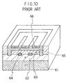
- This bipolar transistor is formed by connecting an internal base layer 64 stradding over the collector layer 62 and collector epitaxial layer 63 on the semiconductor substrate 61 to the base layer 65.
- the carrier injected from the emitter 66 easily recombined in the internal base layer 64, and the carrier life time can be shortened. While, paying attention to the carrier injected in the collector side, when changing over the transistor from ON state to OFF state, the carrier is absorbed by the inverse base current flowing through the internal base layer 64 of low resistance, and is recombined. In this transistor, since the carrier is absorbed through the internal base layer 64 of low resistance, the storage time can be shorter than in the prior art.
- the transistor provided with field limiting ring and field plate in order to heighten the breakdown voltage of transistor they are ususally provided outside the base region, and the number of field limiting rings must be increased in order to have a sufficient breakdown voltage, which requires a wider collector area, resulting in a large chip size.
- the base region is shallow, and a certain high frequency characteristic may be maintained and a high breakdown voltage can be realized, but the minority carrier which is the factor of impeding the high speed switching action of transistor cannot be extracted, and hence the time of the switching is slow.
- the bipolar transistor as shown in Fig. 10 since the minority carrier can be extracted, a high speed switching action can be realized, but since the base region is shallow, the safe operating area (SOA) is narrow, and enhancement of breakdown voltage is insufficient.
- SOA safe operating area
- SOA safe operating area
- the present inventor intensively investigated into the relationship of the impurity concentration of each layer and layer thickness to enhance the breakdown voltage and decrease the saturation voltage V CE (sat), and discovered that the breakdown voltage is enhanced by dividing the collector region into two layers differing in the impurity concentration, and forming the layer of lower impurity concentration at the surface side of semiconductor layer, and that the transistor characteristic can he enhanced, that is, the saturation voltage V CE (sat) is lowered and the switching speed is increased, by defining the impurity concentration in the operating area at an ordinary theoretical concentration.
- the breakdown voltage BV of the transistor is generally expressed as follows:
- the impurity concentration of bulk (collector layer) to be N C
- the radius of curvature to be r j the constant determined by the junction state to be n (this value of n is 1 in a cylindrical junction, 2 in a spherical junction, and ⁇ in a planar junction), and the thickness of base region to be W B .
- the saturation voltage V CE (sat) of the transistor is expressed as follows, supposing the specific resistance of the collector layer to be r C , the thickness of collector layer to be W C , the effective emitter area to be A E , and the collector current to be l C .
- V CE (s a t) ⁇ ⁇ C W C A E ⁇ I C and V CE (sat) is lower as the collector layer specific resistance r c and thickness W C are smaller, and the impurity concentration of collector layer is in the trade-off relation with the condition for enhancing the breakdown voltage.
- the collector layer is divided into two layers, and the both functions are achieved.
- the transistor of the invention comprises:
- the semiconductor substrate because a wider safe operating area is obtained.
- the third semiconductor layer of the same conductive type is formed a much lower impurity concentration. So, the portion likely to break down of the semiconductor layer surface is high in resistance, contribute to enhancement of breakdown voltage, and the semiconductor layer contributing to operation of the transistor inside is formed at an impurity concentration suited to usual transistor operation, and therefore a transistor of high speed switching action is realized at a low saturation voltage.
- the transistor in the second aspect of the invention is a transistor comprising a collector region of first conductive type provided on a semiconductor substrate, a base region of second conductive type provided on the collector region, and an emitter region of the first conductive type provided on the base region, with emitter regions or base regions formed in a plurality of insular forms, in a multi-emitter or multi-base structure comprising of a plurality of unit transistors, wherein each unit transistor is formed so that the thickness of the base region immediately beneath the emitter region may be thinner than the thickness of the base region in the portion free of the emitter region, and hence and the base region is formed in a " ⁇ "-like shaped section, and the internal base layer is formed in each recess of " ⁇ "-like shaped.
- the first conductively type and second conductive type are the first conductive type of either conductive type of n type or p type and the second conductive type of the other p type or n type.
- the " ⁇ "-like shaped section of the base region is formed in at least two adjacent unit transistors continuously, and the internal base layers are formed in the recess of the base region of the adjacent unit transistors, and hence it is preferred because the patterning is easy, the internal of unit transistors can be narrowed, and the chip size can be reduced.
- each internal base layer of the unit transistor is connected with the base region of the unit transistor, it is preferred because the element is further reduced in size.
- the internal base layer is connected to the high concentration impurity region introduced from the surface of the semiconductor substrate, and is connected to the base electrode by wiring, and hence it is connected to the base electrode through the low resistance region of high impurity concentration to the base electrode through the low resistance region of high impurity concentration without passing through the base region of high resistance, so that the carrier is the semiconductor of quick, which is preferred for switching operation at high speed.
- the base region immediately beneath the emitter region of each unit transistor is formed thinly, and an internal base layer is provided beneath it, so that the current amplification factor h FE and transition frequency f T depending on the thickness of the base region can be increased, while the residual carrier in the collector region can be absorbed in a short time by the internal base layer, so that the switching action becomes faster in speed.
- the base region at both sides immediately beneath the emitter region of each unit transistor is formed thick, and therefore the safe operating area is wide, and the breakdown voltage is enhanced.
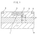
- the transistor of the first aspect of the invention comprises a collector region 1 comprising a second semiconductor layer 1b of n - type of low impurity concentration formed on a first semiconductor layer 1a which is a semiconductor substrate of, for example, n + type, and a third semiconductor layer 1c of same conductive type n - type of further lower impurity concentration than in the second semiconductor layer 1b epitaxially grown on the second semiconductor layer 1b, a base region 2 of, for example, p type formed by diffusion or the like on the third semiconductor layer 1c of the collector region 1, and an emitter region 3, for example, n + type formed by diffusion or the like on the base region 2.
- the second semiconductor layer 1b is provided on the semiconductor substrate by diffusion or epitaxial growth, and is the principal portion of the collector region 1 of the transistor, and its specific resistance is formed around 1 x 10° to 1 x 10 3 ⁇ cm (impurity concentration 5 x 10 12 to 5 x 10 15 /cm 3 ).
- the third semiconductor 1c is formed on the second semiconductor layer 1b by means of epitaxial growth.
- the third semiconductor layer 1c is intended to enhance the breakdown voltage on the semiconductor layer surface, and is formed in a thickness of about several to scores of micrometers at a specific resistance of 1 x 10 1 to 1 x 10 4 l ⁇ cm (impurity concentration 5 x 10 11 to 5 x 10 14 /cm 3 ).
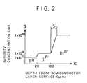
- each semiconductor layer is shown, for exmple, in Fig. 2, in which the depth from the surface of the semiconductor layer is plotted on the x-axis and the impurity concentration Nc on the y-axis.
- the third semiconductor layer 1c, second semiconductor layer 1b, first semiconductor layer 1a are respectively indicated by I, II and III.
- the saturation voltage of the transistor V CE (sat) is set low, and on the second semiconductor layer 1b of low impruity concentration, being such an impurity concentration as to obtain a high speed switching, the third semiconductcor layer 1c of the same conductive type is formed at a further lower impurity concentration than that of the second semiconductor layer 1b is provided by epitaxial growth, thereby forming the collector region 1.
- the resistance portion of the collector region 1 is the sum R 1 + R 2 of resistance R 1 of the third semiconductor layer 1c between the bottom of the base region 2 and the second semiconductor layer 1b and resistance R 2 of the second semiconductor layer 1b.
- the specific resistance of the third semiconductor layer 1c is about 2 to 10 times as large as that of the second semiconductor layer 1b, but the thickness H 1 is thin between the bottom of the base region 2 and the second semiconductor layer 1b, being about 1/10 of thickness of thickness H 2 of the second semiconductor layer 1b, and the resistance R 1 is smaller than the resistance R 2 , and hence the resistance of the collector region 1 is nearly determined by R 2 . Further, the base region 2 may be diffused up to the second semiconductor layer. In this case, the resistance R 1 is eliminated.
- the specific resistance of the second semiconductor layer 1b so as to be a theoretical value, a transistor of fast switching speed is obtained at a low saturation voltage.
- this portion is formed of the third semiconductor layer 1c which is low in the impurity concentration and high in specific resistance, it is resistant to breakdown as known from formula (1), and a transistor of high breakdown voltage is obtained on the whole.
- the impurity concentration of the third semiconductor layer of 1c resistant to breakdown and not adversely affecting the transistor characteristic is about 5 x 10 11 to 5 x 10 14 /cm 3 (specific resistance 1 x 10 1 to 1 x 10 4 l ⁇ cm).
- the impurity concentration it too low, the resistance R 1 is too large for the collector region 1 beneath the base region 2 and the saturation voltage V CE (sat) is too large, and the switching speed drops, or if the impurity concentration is too high, it is less resistant to breakdown, and high breakdown voltage is not obtained.
- the depletion layer for breakdown voltage may be thin, and the third semiconductor layer 1c is formed in a thickness of about 10 to 50 ⁇ m, and the base region 2, in thickness of about 5 to 100 ⁇ m.
- the thickness of the base region 2 is desired to be greater, but if the thickness of the base region 2 is reduced to such thinness, a sufficient breakdown voltage is assured, since the breakdown voltage is increased by lowering the impurity concentration. As a result, the base region 2 is thin and the diffusion time for forming the base region is cut short, so that the cost may be reduced.
- the semiconductor substrate comprising the second semiconductor layer 1b may be either a diffusion semiconductor substrate using, for example, an n - type semiconductor substrate of low impurity concentration as second semiconductor substrate 1b, and introducing an n type impurity further on the back side to form an n + type first semiconductor layer 1a, or an epitaxial growth substrate having an n - type second semiconductor layer 1b epitaxially grown on the surface of the semiconductor substrate made of an n + type first semiconductor layer.
- the diffusion semiconductor substrate is modest in the boundary of impurity concentration (see S in Fig. 2) between the second semiconductor layer 1b and first semiconductor layer 1a, and is resistant to short pulses and broad in safe operating area, which is very preferable.
- the epitaxial growth substrate is steep in the boundary of impurity concentration.
- a high breakdown voltage is achieved by disposing a semiconductor layer of high resistance of semiconductor layer, but it can be also used together with the field limiting ring or field plate employed hitherto.
- the element dividing area around the transistor, and annular region 6 is provided same as in the prior art.
- an n type impurity such as arsenic, phosphorus and antimony is diffused to form an n + type first semiconductor layer 1a.
- the thickness of the second semiconductor layer 1b is about 40 to 200 ⁇ m, or preferably 60 to 150 ⁇ m. If too thick, V CE (sat) becomes too large, whereas if too thin, high breakdown voltage is not obtained due to punch-through.
- an n -- type third semiconductor layer 1c of lower impurity concentration about 5 x10 11 to 5x 10 14 /cm 3 is provided by epitaxial growth in about 10 to 50 ⁇ m, or preferably 15 to 30 ⁇ m (see Fig. 3 (a)).
- a p type base layer 2 is formed by ion implantation or diffusion method (Fig. 3 (b)).
- a field limiting ring it is formed simultaneously with the base region 2.
- an impurity such as phosphorus is injected, and an n + type emitter region 3 is formed.
- insulation film is provided on the surface of the semiconductor layer, and a contact hole is formed on the insulation film, a base electrode is provided on the upper part of the base region 2, and an emitter electrode from the emitter region 3, and the electrodes are wired to fabricate a transistor.
- npn transistor is mentioned above, but the invention is similarly applicable to the pnp transistor of inverted conductive type or MOS type field effect transistor. After further disposing a low resistance layer on the third semiconductor layer 1c, the transistor may be formed.
- the collector region comprises of a semiconductor layer of such impurity concentration as to be preferable for the transistor operation and specific resistance for theoretical breakdown voltage, and a semiconductor layer of low impurity concentration of high specific resistance provided at the surface side, a high speed switching characteristic is obtained at a low saturation voltage, and the transistor of high breakdown voltage is obtained by the semiconductor layer of low impurity concentration at the surface side.
- the depletion layer width necessary for achieving breakdown voltage may be narrow, so that the high resistance layer may be made thin, and the base layer may be shallow, and hence the diffusion time can be curtailed.
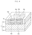
- a multi-emitter transistor comprises of plural unit transistors, comprising a collector region 11 of first conductive type of, for example, n - type epitaxially grown on a semiconductor substrate, a base region 12 of second conductive type of, for example, n type formed by diffusion or the like on the collector region 11, and multi-emitter regions 13 (13a, 13b, ⁇ ) of first conductive type of, for example, n type, formed in a plurality of insular forms by diffusion or the like the base region 12.
- Each unit transistor is provided with internal base layers 14 (14a, 14b, ⁇ ) of second conductive type of, for example, p + type, and the internal base layers 14a ⁇ arranged in each row are provided consecutively, and diffusion regions 15 (15a, 15b, ⁇ ) of high concentration impurity conducting with the surface of the semiconductor layer of the same conductive type as the internal base layers 14, for example, p + type are disposed at the end portion.
- the base region 12 is, as shown in Fig. 4, formed thick in the surrounding of each unit transistor toward the inside of the semiconductor layer, and thin in the central part beneath the emitter region, and the section has " ⁇ "-like shape.
- the internal base layers 14 penetrate through the collector region 11 in the " ⁇ "-like shaped recess of the base region 12, and are connected with the p + diffusion regions 15 (15a, 15b, ⁇ ) communicating with the surface of the semiconductor layer where unit transistors are not formed. They are further connected to the base electrode pads by the wiring provided through the insulating layer (not shown) on the semiconductor surface.
- the internal base layers 14 may be also connected directly with the base regions 12 through semiconductor layer, without being once led out onto the substrate surface through the diffusion regions 15. By connecting to the base electrode pads through the diffusion regions 15, the base regions 12 of large resistance can be skipped, so that the residual carrier can be eliminated earlier, but when directly connected to the base regions 12, the chip area can be reduced. If diffusion regions 15 are not provided, it is preferred to form the " ⁇ "-sections of the base regions adjacent unit transistors continuously and form also the internal base regions 14 continuously because it is not necessary to connect the internal base layers 14 and base regions 12 in ecah unit transistor. Examples of continuous form of internal base layers 14 are shown in Fig. 5(a) and (b).
- Fig, 5(a) shows an example of internal base layers 14 provided continuously to unit transistors arranged in a row
- Fig. 5(a) shows an example of coupling each unit transistor with a square ring
- Figs. 5(b) shows an example of coupling each unit transistor with a square ring
- FIG. 6 A plane explanatory diagram of base electrode and emitter electrode of the multi-emitter transistor is given in Fig. 6, in which base contacts 17 and emitter contacts 18 are provided on the base regions and multi-emitter regions through openings formed in the insulating film, and are further connected respectively to the base electrode wiring 19 and emitter electrode wiring 20, and connected to the base pads 21 and emitter pads 22.
- the layers of the base regions 2 beneath the multi-emitter regions 13 (13a, 13b, ⁇ ) which are unit trasistors are formed thin, and internal base layers 14 (14a, 14b, ⁇ ) of high impurity concentration are provided in the collector regions 11 at the lower side of thin base resions 2, and the internal base layers 14 are not directly connected to the base regions 12, but are connected with the base electrode pads through the diffusion regions 15 (15a, 15b, ⁇ ) of high impurity concentration. Accordingly, the carrier remaining in the collector regions can be easily captured by the internal base layers 14 of low resistance, and escapes to the base electrodes through the diffusion regions 5 of low resistance, so that the residual carrier can be immediately eliminated. A a result, the switching speed is fast, and in particular the turn-off time (t off ) from saturation sate to cut-off state can be greatly reduced.
- the base ground current amplification factor h FE is expressed as follows: h FE ⁇ 1 1+ ⁇ B ⁇ E ⁇ W B L h ⁇ 1 1+ 1 2 W B L n 2 where ⁇ B , ⁇ E are the conductivities of base and emitter, respectively, W B is thickness of base region, and L h , L n are the diffusion lengths of minority carrier of holes and electrons, respectively.
- W B is smaller, h FE becomes larger, so that a high current amplification factor h FE is obtained.
- transition frequency f T is expressed as f T ⁇ 1 2 ⁇ ⁇ 2D n W B 2 where Dn is the diffusion coefficient.
- W B is smaller, f T becomes larger, so that a high f T is obtained.
- the safe operating area is narrow because of secondary breakdown.
- the secondary breakdown occurs in forward bias when the voltage drop caused by the base current flowing in the lateral direction causes the base current to be concentrated in the end portion of the emitter regions 13. Hence it may break the transistor down.
- W B of the base regions 12 around the end portion of the emitter regions where the current is likely to be concentrated as much as possible the secondary breakdown is suppressed, and the safe operating area are can be broadened.
- the thickness W B of the base regions 12 beneath the multi-emitter regions 13a, 13b, ⁇ is formed thin so as to obtain a high transition freqeucy f T and high current amplification factor h FE , while the thickness of the outside base regions 12 is formed thick, so that a wide safe operating area and a high breakdown voltage are realized.
- internal base layers 14 of high impurity concentration are formed in the collector regions 11 at the lower side of the thin base regions 12, and are connected with the base regions 12, or connected with the base electrodes on the substrate surface, and hence L h and L n are small in formula (2), and the amplification factor h FE increases, while the minority residual carrier remaining in the collector regions 11 is easily captured in the internal base layer 14 of low resistance, escapes to the base electrodes through the base regions or wiring, so that the residual carrier may be eliminated immediately.
- the switching speed is fast, and especially the turn-off time (t off ) from saturation state to cut-off state is curtailed.
- an n - type epitaxial layer 11b is formed by epitaxial growth to form part of the collector region 11, the base ends 12a, 12b of part of the p type base region 12, and internal base layer 14 are formed in the epitaxial layer 11b by ion implantation, diffusion or other method (see Fig. 7(a)).
- n - type epitaxial layer 11c is formed by epitaxial growth, and the collector region 11 is formed (see Fig. 7 (b)). Since the temperature elevates at this time of epitaxial growth, the impurities of the base ends 12a, 12b and internal base layers 14a, 14b diffuse in the growing epitaxial layer 11c, and slightly spread upward.
- the base ends connected to the base ends 12a, 12b, the base region 12 between them, and the diffusion region (not shown) connected with the internal layer 14 adjacently to the base region 12 are formed (see Fig. 7 (c)).
- the upper parts of the base ends 12a, 12b are formed deep so as to be connected with the base ends 12a, 12b at the end portion of the base regions 12, and the intermediate middle parts are formed shallow so as not to connect with the internal base layers 14a, 14b, and thereby a " ⁇ "-like shaped section is formed as shown in Fig. 7(c).
- the shallow portion is a depth of about, for example, 1 to 20 ⁇ m, and the deep portion is about 5 to 50 ⁇ m.
- the diffusion process is divided into two steps, and the impurities are introduced separately into the end portion and central portion, or impurities of different diffusion speed are used, for example, aluminium and arsenic, and the aluminium of fast diffusion speed is applied in the end portion while the arsenic of slow diffusion speed in the central portion, diffusing at about 950°C to 1380°C, and in the same diffusion time, the aluminium of fast diffusion speed diffuses to a greater depth, thereby forming the base region 1 as shown in Fig. 7(c).
- the depth of the impurity region can be adjusted by controlling the ion implantation energy.
- n + emitter regions 13a, 13b are formed (see Fig. 7(d)).
- contact holes are formed in the insulation film provided on the surface of the semiconductor layer, electrodes are provided in each region, and the electrodes are wired.
- npn transistor explained in the embodiment, but it is the same with the pnp transistor of inverted conductive type.
- the shape of the base region and diode is not limited to the explained example.
- the illustrated example of the multi-base transistor it is the same with the multi-emitter transistor.
- the breakdown voltage may be furhter enhanced.
- the base regions are formed thin immediately beneath the emitter regions of unit transistors of multi-base transistor of multi-emitter transistor, and internal base layers are formed at the lower side thereof, and hence the current amplification factor h FE and current gain band width product f T can be enhanced, while the minority carrier implanted into the collector regions flows into the base side through the internal bases in a short time at the time of switching, and is recombined.
- the switching operation is fast, and the time to switch from saturation state to cut-off state is cut short. Accordingly, the power consumption of the electric circuit during the switching time is decreased and heat generation is suppressed, so that the transistor amplification, other characteristics, and reliability can be enhanced.
- the base regions around the emitter regions are formed thick, current concentration is prevented, and the safe operating area can be widened.
- a transistor (a) a first semiconductor layer formed by a semiconductor substrate; (b) a second semiconductor layer formed on the first semiconductor layer and having an impurity of the same conductivity type as the first layer in a concentration lower than that of the first semiconductor layer; and (c) a third semiconductor layer formed on the second semiconductor layer having an impurity of the same conductivity type as the first semiconductor layer in a concentration lower than that of the second semiconductor layer; wherein a base region is formed in the third layer and an emitter region is in the base region.
- the present invention proposes a transistor comprising a collector region of a first conductivity type provided on a semiconductor substrate, a base region of second conductivity type provided on the collector region, and an emitter region of the first conductivity type provided on the base region, with emitter regions or base regions formed in a plurality of insular forms, in a multi-emitter or multi-base structure composed of a plurality of unit transistors, wherein each unit transistor is formed so that the thickness of the base region immediately beneath the emitter region may be thinner than the thickness of the base region in the portion free of the emitter region, and hence the base region is formed in a " ⁇ "-like shaped section, and the internal base layer is formed in each recess of " ⁇ "-like shape.
Landscapes
- Bipolar Transistors (AREA)
Applications Claiming Priority (5)
| Application Number | Priority Date | Filing Date | Title |
|---|---|---|---|
| JP1120994 | 1994-02-02 | ||
| JP01121094A JP3233767B2 (ja) | 1994-02-02 | 1994-02-02 | トランジスタ |
| JP1121094 | 1994-02-02 | ||
| JP6011209A JPH07221116A (ja) | 1994-02-02 | 1994-02-02 | トランジスタ |
| EP95101357A EP0666600B1 (de) | 1994-02-02 | 1995-02-01 | Leistungs-Bipolartransistor |
Related Parent Applications (1)
| Application Number | Title | Priority Date | Filing Date |
|---|---|---|---|
| EP95101357A Division EP0666600B1 (de) | 1994-02-02 | 1995-02-01 | Leistungs-Bipolartransistor |
Publications (3)
| Publication Number | Publication Date |
|---|---|
| EP0921574A2 true EP0921574A2 (de) | 1999-06-09 |
| EP0921574A3 EP0921574A3 (de) | 1999-06-16 |
| EP0921574B1 EP0921574B1 (de) | 2002-09-11 |
Family
ID=26346616
Family Applications (2)
| Application Number | Title | Priority Date | Filing Date |
|---|---|---|---|
| EP99104774A Expired - Lifetime EP0921574B1 (de) | 1994-02-02 | 1995-02-01 | Transistor |
| EP95101357A Expired - Lifetime EP0666600B1 (de) | 1994-02-02 | 1995-02-01 | Leistungs-Bipolartransistor |
Family Applications After (1)
| Application Number | Title | Priority Date | Filing Date |
|---|---|---|---|
| EP95101357A Expired - Lifetime EP0666600B1 (de) | 1994-02-02 | 1995-02-01 | Leistungs-Bipolartransistor |
Country Status (3)
| Country | Link |
|---|---|
| US (1) | US5637910A (de) |
| EP (2) | EP0921574B1 (de) |
| DE (2) | DE69512101T2 (de) |
Cited By (1)
| Publication number | Priority date | Publication date | Assignee | Title |
|---|---|---|---|---|
| WO2008127186A1 (en) * | 2007-04-11 | 2008-10-23 | Transic Ab | Silicon carbide semiconductor device |
Families Citing this family (13)
| Publication number | Priority date | Publication date | Assignee | Title |
|---|---|---|---|---|
| SE511891C2 (sv) * | 1997-08-29 | 1999-12-13 | Ericsson Telefon Ab L M | Bipolär effekttransistor och framställningsförfarande |
| DE10232176A1 (de) * | 2002-07-16 | 2004-02-05 | Infineon Technologies Ag | Bipolarer Hochfrequenztransistor und Verfahren zur Herstellung desselben |
| CN101868856B (zh) | 2007-09-21 | 2014-03-12 | 飞兆半导体公司 | 用于功率器件的超结结构及制造方法 |
| US20120273916A1 (en) | 2011-04-27 | 2012-11-01 | Yedinak Joseph A | Superjunction Structures for Power Devices and Methods of Manufacture |
| US8786010B2 (en) | 2011-04-27 | 2014-07-22 | Fairchild Semiconductor Corporation | Superjunction structures for power devices and methods of manufacture |
| US8836028B2 (en) | 2011-04-27 | 2014-09-16 | Fairchild Semiconductor Corporation | Superjunction structures for power devices and methods of manufacture |
| US8673700B2 (en) | 2011-04-27 | 2014-03-18 | Fairchild Semiconductor Corporation | Superjunction structures for power devices and methods of manufacture |
| US8772868B2 (en) | 2011-04-27 | 2014-07-08 | Fairchild Semiconductor Corporation | Superjunction structures for power devices and methods of manufacture |
| CN103378138B (zh) * | 2012-04-18 | 2016-12-14 | 朱恩均 | 双极晶体管及其制作方法 |
| US20150118810A1 (en) * | 2013-10-24 | 2015-04-30 | Madhur Bobde | Buried field ring field effect transistor (buf-fet) integrated with cells implanted with hole supply path |
| US20180026122A1 (en) * | 2015-10-09 | 2018-01-25 | Ideal Power Inc. | B-TRAN Geometry and Structure That Provides Both High Gain and High Current Density |
| CN111370497A (zh) * | 2020-04-24 | 2020-07-03 | 济南兰星电子有限公司 | 半导体台面二极管芯片及其制作方法 |
| CN118073459B (zh) * | 2024-04-18 | 2024-08-23 | 中国科学院宁波材料技术与工程研究所 | 一种光电晶体管及其制备方法 |
Family Cites Families (12)
| Publication number | Priority date | Publication date | Assignee | Title |
|---|---|---|---|---|
| JPS5336481A (en) * | 1976-09-17 | 1978-04-04 | Toshiba Corp | Semiconductor device |
| DE3131611A1 (de) * | 1981-08-10 | 1983-02-24 | Siemens AG, 1000 Berlin und 8000 München | Epitaxialer transistor |
| FR2543736B1 (fr) * | 1983-03-31 | 1986-05-02 | Thomson Csf | Procede de fabrication d'un transistor de puissance a tenue en tension elevee a l'ouverture |
| EP0133339A3 (de) * | 1983-07-29 | 1985-03-20 | Trw Inc. | Silicid-Bipolartransistor und Verfahren zum Herstellen dieses Transistors |
| JPS60160165A (ja) * | 1984-01-31 | 1985-08-21 | Shindengen Electric Mfg Co Ltd | バイポ−ラトランジスタ |
| JPS60175453A (ja) * | 1984-02-20 | 1985-09-09 | Matsushita Electronics Corp | トランジスタの製造方法 |
| JPH0193167A (ja) * | 1987-10-05 | 1989-04-12 | Toyota Autom Loom Works Ltd | 高耐圧トランジスタ |
| JPH01232742A (ja) * | 1988-03-11 | 1989-09-18 | Fujitsu Ltd | 半導体装置 |
| IT1234517B (it) * | 1988-05-05 | 1992-05-19 | Sgs Thomson Microelectronics | Dispositivo a semiconduttore bipolare di potenza e procedimento per la sua fabbricazione |
| US5221856A (en) * | 1989-04-05 | 1993-06-22 | U.S. Philips Corp. | Bipolar transistor with floating guard region under extrinsic base |
| EP0609351A4 (de) * | 1991-10-23 | 1995-01-04 | Microunity Systems Eng | Bopolartransistor mit verbesserten stromverstärkungs- und durchbruchcharakteristiken. |
| JPH0637098A (ja) * | 1992-07-15 | 1994-02-10 | Hitachi Ltd | 半導体装置及びその製造方法 |
-
1995
- 1995-02-01 US US08/382,393 patent/US5637910A/en not_active Expired - Lifetime
- 1995-02-01 EP EP99104774A patent/EP0921574B1/de not_active Expired - Lifetime
- 1995-02-01 DE DE69512101T patent/DE69512101T2/de not_active Expired - Lifetime
- 1995-02-01 EP EP95101357A patent/EP0666600B1/de not_active Expired - Lifetime
- 1995-02-01 DE DE69528203T patent/DE69528203T2/de not_active Expired - Lifetime
Cited By (2)
| Publication number | Priority date | Publication date | Assignee | Title |
|---|---|---|---|---|
| WO2008127186A1 (en) * | 2007-04-11 | 2008-10-23 | Transic Ab | Silicon carbide semiconductor device |
| US8829533B2 (en) | 2007-04-11 | 2014-09-09 | Fairchild Semiconductor Corporation | Silicon carbide semiconductor device |
Also Published As
| Publication number | Publication date |
|---|---|
| EP0666600B1 (de) | 1999-09-15 |
| DE69528203T2 (de) | 2003-07-31 |
| EP0921574B1 (de) | 2002-09-11 |
| US5637910A (en) | 1997-06-10 |
| EP0666600A3 (de) | 1996-04-10 |
| DE69528203D1 (de) | 2002-10-17 |
| DE69512101T2 (de) | 2000-04-27 |
| EP0666600A2 (de) | 1995-08-09 |
| EP0921574A3 (de) | 1999-06-16 |
| DE69512101D1 (de) | 1999-10-21 |
Similar Documents
| Publication | Publication Date | Title |
|---|---|---|
| CA2286699C (en) | Latch-up free power mos-bipolar transistor | |
| EP0009367B1 (de) | Durch eine Steuerelektrode abschaltbarer Thyristor | |
| US5637910A (en) | Multi-emitter or a multi-base transistor | |
| US4975751A (en) | High breakdown active device structure with low series resistance | |
| KR100397882B1 (ko) | 전계효과-제어가능반도체소자 | |
| US4901120A (en) | Structure for fast-recovery bipolar devices | |
| US4315271A (en) | Power transistor and method of manufacturing same | |
| US5091336A (en) | Method of making a high breakdown active device structure with low series resistance | |
| US3460009A (en) | Constant gain power transistor | |
| EP0632502B1 (de) | Bipolar-Leistungstransistor mit hoher Kollektor-Durchbrucksspannung und Verfahren zu seiner Herstellung | |
| EP0086210B1 (de) | Diode für monolithische integrierte schaltung | |
| US4027324A (en) | Bidirectional transistor | |
| EP0064613A2 (de) | Halbleiteranordnung mit einer Verschiedenheit von Elementen, die parallel funktionieren | |
| GB2184599A (en) | Schottky diode for an integrated circuit | |
| EP0064614B1 (de) | Emitterstruktur für Halbleiteranordnungen | |
| JPH06104459A (ja) | 半導体装置 | |
| EP0180315B1 (de) | Halbleiteranordnung mit hoher Durchbruchspannung | |
| US4825270A (en) | Gate turn-off thyristor | |
| WO2000035018A1 (en) | Sidewall junction for bipolar semiconductor devices | |
| US20250374659A1 (en) | Integrated circuit device including bipolar junction transistor | |
| JPS6327865B2 (de) | ||
| JPH11204804A (ja) | 半導体装置 | |
| JPH0416443Y2 (de) | ||
| JP3233767B2 (ja) | トランジスタ | |
| JP3146024B2 (ja) | 半導体装置 |
Legal Events
| Date | Code | Title | Description |
|---|---|---|---|
| PUAI | Public reference made under article 153(3) epc to a published international application that has entered the european phase |
Free format text: ORIGINAL CODE: 0009012 |
|
| PUAL | Search report despatched |
Free format text: ORIGINAL CODE: 0009013 |
|
| AC | Divisional application: reference to earlier application |
Ref document number: 666600 Country of ref document: EP |
|
| AK | Designated contracting states |
Kind code of ref document: A2 Designated state(s): DE FR GB |
|
| AK | Designated contracting states |
Kind code of ref document: A3 Designated state(s): DE FR GB |
|
| 17P | Request for examination filed |
Effective date: 19990906 |
|
| 17Q | First examination report despatched |
Effective date: 20010516 |
|
| GRAG | Despatch of communication of intention to grant |
Free format text: ORIGINAL CODE: EPIDOS AGRA |
|
| GRAG | Despatch of communication of intention to grant |
Free format text: ORIGINAL CODE: EPIDOS AGRA |
|
| GRAH | Despatch of communication of intention to grant a patent |
Free format text: ORIGINAL CODE: EPIDOS IGRA |
|
| GRAH | Despatch of communication of intention to grant a patent |
Free format text: ORIGINAL CODE: EPIDOS IGRA |
|
| GRAA | (expected) grant |
Free format text: ORIGINAL CODE: 0009210 |
|
| AC | Divisional application: reference to earlier application |
Ref document number: 666600 Country of ref document: EP |
|
| AK | Designated contracting states |
Kind code of ref document: B1 Designated state(s): DE FR GB |
|
| REG | Reference to a national code |
Ref country code: GB Ref legal event code: FG4D |
|
| REF | Corresponds to: |
Ref document number: 69528203 Country of ref document: DE Date of ref document: 20021017 |
|
| ET | Fr: translation filed | ||
| PLBE | No opposition filed within time limit |
Free format text: ORIGINAL CODE: 0009261 |
|
| STAA | Information on the status of an ep patent application or granted ep patent |
Free format text: STATUS: NO OPPOSITION FILED WITHIN TIME LIMIT |
|
| 26N | No opposition filed |
Effective date: 20030612 |
|
| PGFP | Annual fee paid to national office [announced via postgrant information from national office to epo] |
Ref country code: FR Payment date: 20120221 Year of fee payment: 18 |
|
| PGFP | Annual fee paid to national office [announced via postgrant information from national office to epo] |
Ref country code: DE Payment date: 20120125 Year of fee payment: 18 |
|
| PGFP | Annual fee paid to national office [announced via postgrant information from national office to epo] |
Ref country code: GB Payment date: 20120201 Year of fee payment: 18 |
|
| GBPC | Gb: european patent ceased through non-payment of renewal fee |
Effective date: 20130201 |
|
| REG | Reference to a national code |
Ref country code: FR Ref legal event code: ST Effective date: 20131031 |
|
| REG | Reference to a national code |
Ref country code: DE Ref legal event code: R119 Ref document number: 69528203 Country of ref document: DE Effective date: 20130903 |
|
| PG25 | Lapsed in a contracting state [announced via postgrant information from national office to epo] |
Ref country code: DE Free format text: LAPSE BECAUSE OF NON-PAYMENT OF DUE FEES Effective date: 20130903 Ref country code: FR Free format text: LAPSE BECAUSE OF NON-PAYMENT OF DUE FEES Effective date: 20130228 Ref country code: GB Free format text: LAPSE BECAUSE OF NON-PAYMENT OF DUE FEES Effective date: 20130201 |