EP0919846A2 - Aufzeichnungsabtaster mit abnehmbaren Kollimator - Google Patents
Aufzeichnungsabtaster mit abnehmbaren Kollimator Download PDFInfo
- Publication number
- EP0919846A2 EP0919846A2 EP98122005A EP98122005A EP0919846A2 EP 0919846 A2 EP0919846 A2 EP 0919846A2 EP 98122005 A EP98122005 A EP 98122005A EP 98122005 A EP98122005 A EP 98122005A EP 0919846 A2 EP0919846 A2 EP 0919846A2
- Authority
- EP
- European Patent Office
- Prior art keywords
- raster output
- collimator assembly
- output scanner
- light beam
- scanner housing
- Prior art date
- Legal status (The legal status is an assumption and is not a legal conclusion. Google has not performed a legal analysis and makes no representation as to the accuracy of the status listed.)
- Granted
Links
Images




Classifications
-
- G—PHYSICS
- G02—OPTICS
- G02B—OPTICAL ELEMENTS, SYSTEMS OR APPARATUS
- G02B26/00—Optical devices or arrangements for the control of light using movable or deformable optical elements
- G02B26/08—Optical devices or arrangements for the control of light using movable or deformable optical elements for controlling the direction of light
- G02B26/10—Scanning systems
- G02B26/12—Scanning systems using multifaceted mirrors
- G02B26/127—Adaptive control of the scanning light beam, e.g. using the feedback from one or more detectors
Definitions
- This invention relates generally to raster scanning systems and more particularly, to a raster output scanner which utilizes a collimator assembly which can be replaced in the field at a customer location without disassembling the raster output scanner and sending it back to the manufacturer for replacement.
- a laser printer utilizes a raster output scanner.
- the raster output 10 utilizes a laser light source 12, a collimator 14, mirrors 16 and 18, pre-polygon optics 20 and 22, mirror 24 a multi-faceted rotating polygon mirror 26 as the scanning element, post polygon optics 28, mirror 30 and a photosensitive medium (photoreceptor) 32.
- the laser light source 12 sends a light beam 34 to the rotating polygon mirror 26 through the collimator 14 and the pre-polygon optics 20 and 22.
- Mirrors 16, 18 and 24 fold and redirect the light beam 34 prior to the scanning polygon 26 and mirror 30 folds and redirects the light beam 34 after the scanning polygon 26.
- Mirror 30 is slanted to redirect the light beam 34 outside of the ROS housing onto the photoreceptor 22 to scan a line S.
- the collimator 14 collimates the light beam 34 and the pre-polygon optics 20 focuses the light beam 34 in the sagittal or cross-scan plane onto the rotating polygon mirror 26.
- the light beam stays collimated in the tangential plane while striking the polygon mirror 26.
- the facets 36 of the rotating polygon mirror 26 reflect the light beam 34 and also cause the reflected light beam 34 to revolve about an axis near the reflection point of the facet 36.
- the reflected light beam 34 is utilized through the post polygon optics 28 to scan the photoreceptor 32.
- ROS Raster Output Scanner
- ROS housings 38 is usually made of plastic or metal and has an opening 42 for receiving a light beam from the laser light source 12.
- the collimator assembly 40 holds the laser diode 12 and the collimator 14.
- the base 46 of the collimator assembly 40 is mounted on wall 44 of the housing 38 in such a manner that the axis 48 of the collimator assembly coincides with optical path 35.
- the optical path 35 is the optical axis of the optical elements within the ROS housing 38.
- the laser diode 12 emits a light beam 34 and collimator 14 collimates and sends the light beam 34 into the ROS housing 38 through the opening 42. Within the ROS housing 38, the light beam 34 travels along the optical path 35.
- the position of the light beam 34 from the laser diode has to be adjusted to overlap the optical path 35 and the intensity of the light beam 34 has to be adjusted to match a required discharge level of the photoreceptor used in that specific printer. Adjusting the position and the intensity of the light beam 34 are very critical in the print quality. For example, if the light beam 34 does not travel on the optical path 35, the light beam striking the photoreceptor might be out of focus which causes the print to be blurred. In addition, if the intensity level of the light beam happens to be over or under the required level, the print will be darker or blank respectively.
- the above adjustments are done based on the location and the characteristics of the laser diode.
- the pointing of a laser diode with respect to the optical path 35 depends on the mounting of the collimator assembly to the ROS housing. Furthermore, characteristics of each individual laser diode is different from characteristics of other laser diodes. Therefore, in order to adjust the intensity of a laser diode, the laser driving current has to be adjusted. As a result, if a laser diode of a printer needs to be replaced, the whole ROS housing is used to readjust a new replacement collimator assembly.
- the ROS housing including the collimator assembly
- the ROS housing has to be dismounted from the printer and sent back to the manufacturing. Since the ROS housing holds expensive optical elements, it is desirable not to transfer it back to manufacturing to prevent any damage to the optical elements. Furthermore, transferring the ROS housing to the manufacturing for repair or replacement can be very costly to the user in terms of loss of productivity. Therefore, it is advantageous to replace the collimator assembly in the field instead of sending the ROS housing back to the manufacturer.
- the object of the present invention is solved by apparatus having the features described in claim 1, 7 and 10, respectively.
- the present invention is directed to a design implementation of raster output scanner with a field replaceable collimator assembly containing a laser diode.
- the collimator assembly of this invention which acts as a pointing device, is removeably mounted on a raster output housing.
- the design of the collimator assembly and the raster output housing both have aligning means and securing means designed in such a manner that once the aligning means are engaged, the collimator assembly can be slightly moved in the tangential plane to align the securing means. Once the securing means are engaged, the light beam from the collimator is in alignment with an optical path within the raster output housing.
- This invention provides a collimator assembly, which can be replaced and adjusted automatically in the field without the need to transfer the expensive parts back to the manufacturer for replacement.
- the collimator assembly of this invention is designed in such a manner that once the base is mounted on the ROS housing, the light beam from the laser diode in the collimator assembly will be precisely aligned to the optical path of the ROS housing.
- collimator assembly shall mean “a collimator assembly which contains a laser diode”.
- this invention provides a microchip for each collimator assembly.
- Each microchip contains the information about the characteristics of the laser diode used in its respective collimator assembly.
- its respective microchip on the laser controlling electronics has to be replaced to create a new set of currents that match the characteristics of the new laser diode.
- the new set of currents once applied to the new laser diode will cause the laser diode to produce the original ROS exposure levels.
- the design of the ROS housing and the laser driving electronics are modified to accept the newly designed collimator assembly of this invention and its microchip.
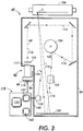
- FIG 3 there is shown a tangential view of a raster output scanner 49 of this invention and referring to Figure 4, there is shown a collimator assembly 52 and a portion of the ROS housing 50 of Figure 3.
- the collimator assembly 52 is rotated away from the ROS housing 50 to show the base 54 of the laser assembly, which has to be mounted on the wall 56 of the ROS housing 50.
- the collimator assembly 52 of this invention is designed to have a highly precise relationship between its optical axis 58 and its base 54.
- the base 54 of the collimator assembly 52 and the ROS housing 50 have a design in such a manner that once the collimator assembly 52 is mounted on the ROS housing 50, the optical axis 58 will be aligned with the optical path 60 (optical axis of the optical elements within the ROS housing 50).
- the collimator assembly 52 has a cylindrical housing 62, which receives a laser diode fixture 64 and a lens barrel 66.
- the laser diode fixture 64 which holds a laser diode 68, is aligned with respect to the optical axis 58 of the cylindrical housing 62 in such a manner that the center ray of the light beam 155 of the laser diode 68 coincides with the optical axis 58.
- the laser fixture 64 is aligned with respect to the optical axis 58, the laser fixture 64 will be secured to the cylindrical housing 62 by any well-known means such as screw or adhesive.
- the inner surface 70 of the cylindrical housing 62 has a cylindrical surface 72 which has a radius r 1 which is smaller than the radius r 2 of the inner surface 70 of the cylindrical housing 62.
- the inner surface 70 of the cylindrical housing 62 also has a threaded portion 74.
- the outer surface 76 of the lens barrel 66 has a surface 78 which has a radius r 3 which is larger than the radius r 4 of the outer surface 76, smaller than the radius r 5 of the peaks 80 of the threaded portion 74 and slightly smaller than the radios r 1 of the surface 72.
- the radius r 3 of the surface 78 is designed in such a manner to contact surface 72.
- the outer surface 76 of the lens barrel 66 has a threaded portion 82 to engage the threads of the thread portion 74 of the cylindrical housing 62.
- Surfaces 72 and 78 are designed in such a manner that once they are in contact with each other, the axis 84 of the lens barrel 66 coincides with the axis 58 of the cylindrical housing 62. Threads of the threaded portions 74 and 82 are designed to keep the surfaces 72 and 78 in a fixed position.
- FIG. 6 there is shown a base view of the collimator assembly 52.
- the base 54 of the collimator assembly 52 will be mounted on the wall 56 of the ROS housing 50 of Figures 3 and 4.
- the base 54 has two slots 86 and 88.
- the center lines C 1 and C 2 of the slots 86 and 88 respectively are located on a tangential plane P of Figure 4 which holds the two optical axis 58 and 84.
- Each one of the slots 86 and 88 receives one of the pins 90 and 92 of the ROS housing 50.
- the two slots 86 and 88 are built with a high precision to receive the pins 90 and 92.
- the design of the slots 86 and 88 provide a high precision in the sagittal plane to prevent any movement of the pins 90 and 92 in the sagittal plane in order to align the optical axis 58 of the collimator assembly 52 with the optical path 60 of the ROS housing 50.
- the slots 86 and 88 accommodate enough space for a slight movement of the pins 90 and 92 in the tangential plane along the optical axis 58.
- the purpose of having enough space for the movement of the pins 90 and 92 within slots 86 and 88 respectively is to provide flexibility for the alignment of holes 94, 96 and 98 of the base 54 to the holes 100, 102 and 104 of the ROS housing 50 respectively. Since the collimator assembly sends out a collimated light beam, the movement of the collimator assembly in the tangential plane has minimal effect on the characteristics of the light beam exiting the collimator assembly. However, if the collimator assembly moves in the sagittal direction the alignment of the optical axis 58 of the collimator assembly 52 and the optical path 60 of the ROS housing 50 will be disturbed. Therefore, the slots 86 and 88 are designed to fix the position of the collimator assembly 52 in the sagittal plan once they receive the two pins 90 and 92.
- the alignment of holes 94, 96 and 98 to the holes 100, 102, 104 require a slight movement of the collimator assembly along the optical path 60 of the ROS housing while the pins 90 and 92 are within the slots 86 and 86.
- the collimator assembly 52 will be fixed to the ROS housing by using a first screw through the holes 94 and 100, a second screw through the holes 96 and 102 and a third screw through the holes 98 and 104.
- the holes 100, 102 and 104 have threads to receive the threads of their respective screws.
- the screws used to mount the collimator assembly 52 to the ROS housing 50 can be replaced by any replaceable means, which can mount the collimator assembly 52 to the ROS housing 50.
- the center ray of the laser light beam still did not precisely align with the optical path 60 of the ROS housing 50.
- the problem was caused by the optical elements of a conventional ROS system.
- a conventional ROS housing such as housing 38
- the light beam 34 from the collimator assembly 40 has to travel through several magnifying optical elements such as elements 20.
- the magnifying optical elements 20 are required to produce a wide beam in order to cover at least one facet 36 of a polygon 26.
- ROS system shall mean, "overfilled ROS system”.
- any slight error in the position of light beam from the collimator assembly will be magnified by several magnifying optics, which may cause pointing error that results in laser exposure degradation. Due to the tolerance range of the adjustment of the light beam to the optical axis of the collimator assembly, slight errors in the position of the light beam are inevitable. Even a slight disposition within the tolerance range, once magnified, can cause a major error. Therefore, even if a collimator assembly is precisely mounted on a ROS housing, a disposition within the tolerance range may cause a major error.
- the magnifying optical elements 20 of the conventional ROS housing 38 are moved into the collimator assembly 52 of this invention.
- three lenses 110, 112 and 114 are used in combination to collimate and magnify the light beam 115 of the laser diode 68.
- the lenses 110, 112 and 114 are placed in the collimator assembly 52, the light beam 115 from the laser diode 68 will be collimated with the correct pointing and magnified before exiting the collimator assembly 52 from the exit window 116. As a result, all the elements in the collimator assembly maintain a fixed position with respect to one another. This will keep the exiting light beam at a substantially correct position which reduces the disposition error associated with changing collimator assemblies.
- the ROS system 49 comprises the ROS housing 50 with the collimator assembly 52 mounted thereto along with an electronic circuit board 118 which is connected to the laser diode 68 of the collimator assembly 52 through cable 119.
- aperture 120 limits the width of the light beam 115 exiting from the collimator assembly and entering the ROS housing 50.
- a beam shaping aperture 120 which defines an elliptical opening 121.
- Beam shaping aperture 120 is needed to limit the width of the light beam to W in order to create a proper spot size on the photoreceptor.
- the post polygon optics 122 focuses the reflected light beam 115 from the polygon 124 onto the photoreceptor 126.
- the light beam 115 is shown by its center ray and after mirror 135, it is shown by its outer rays. If the width of the light beam 115 is too wide or too narrow, the spot size on the photoreceptor will be different than the required spot size.
- the width of the light beam at the polygon facet 125 has to be at a given width to produce a given spot size. Since the magnifying lenses are placed in the collimator assembly 52, if the collimator assembly is replaced, due to the tolerances of the lenses, the magnification factor might be slightly different on each collimator assembly. As a result, in order to create a given width light beam, the aperture 120 is placed inside the ROS housing 50 to clip the width of the light beam to the given width W.
- each individual collimator assembly has a dedicated microchip.
- the characteristics of the laser diode of each collimator assembly are stored in the respective microchip.
- mapping Applying a certain current to the laser diode to create certain exposure level on the photoreceptor is called mapping.
- Level 130 represents the minimum level of exposure, which discharges the photoreceptor. Any exposure level below level 130 does not affect the charges on the photoreceptor.
- Level 132 represents the maximum exposure level. Any exposure level above level 132 over exposes the photoreceptor, which causes the pixel to become undesirably darker or lighter depending on the type of xerographic system. However, it may end up over driving the laser diode and gradually damaging the laser diode.
- lines a and b show the characteristics (exposure lines) of two different laser diodes a and b respectively.
- the slope of the exposure line of each laser diode is different than the slope of the exposure line of other laser diode. Therefore, in order to achieve the same exposure levels required by the photoreceptor, each laser diode requires different currents. For example, diode a requires a 1 mA to create the minimum exposure level and diode b requires b 1 mA to create the minimum exposure level. In the same manner, diode a requires a 2 mA to create the maximum exposure level and diode b requires b 2 mA to create the maximum exposure level.
- the difference between the minimum exposure level and the maximum exposure level is divide by 255 to create 255 exposure levels.
- each one of these exposure levels requires a different current.
- different currents may have to be applied to the new laser diode to produce the original ROS exposure set up.
- microchip 134 which is located on circuit board 118, has to be replaced.
- the replacement microchip 134 contains the information about the characteristics of the new laser diode.
- the program in the printer needs to use the characteristic information from the microchip to update laser diode current lookup tables.
- the data in the microchip provides information about the slope and the starting point of the slope of the exposure line of the laser diode.
- the subroutine can be activated either by pushing certain buttons on the interface of the printer or the microprocessor can have a detection scheme to detect the microchip replacement and activate the subroutine automatically.
- the diagnostic subroutine is programmed in a microprocessor 123 which is connected to the electronic circuit board 118. Once activated, the diagnostics subroutine will access the newly placed microchip and retrieves the data. Then, the subroutine uses the data from the microchip to activate the laser diode. Subsequently, it measures the minimum and maximum exposure levels of the light beam from the laser diode at the photoreceptor.
- a portion of the light beam 115 is being deflected by a mirror 136 onto a scan detector 138.
- Scan detector 138 is connected to the electronic circuit 118 through cable 140.
- subroutine The role of subroutine is to receive the measured exposure level of the laser diode 68 at the photoreceptor 126 from the scan detector 138 and compare it to a required maximum exposure level. Then, the diagnostic subroutine has to adjust the current of the laser diode 68 to cause the maximum exposure level of the light beam 115 at the photoreceptor 126 to match the required maximum exposure level. Once the required maximum exposure level is established, the current will be measured and recorded. The subroutine has to perform the same function for the minimum current and record the current.
- the subroutine divides the difference between the minimum and maximum current by 256 to determine the current levels, which can produce different shades of exposure.
- the 255 current levels as well as the minimum and maximum current levels will be stored in a lookup table such as a random access memory (RAM) 142 by over writing the current values, which were used for the previous laser diode.
- RAM random access memory
- the disclosed invention provides a fast, efficient, and cost effective solution to repair large laser printers since it eliminates the down time during which the parts have to be transferred to the manufacturer, the need for transferring expensive parts from the field to the manufacturer and back or the need to carry expensive parts for every repair call.
- the preferred embodiment of this invention has been designed for a field replaceable collimator assembly having an integrated laser diode.
- the concept of the replaceable microchip containing the characteristics of its respective laser diode can also be applied to a raster output scanner with a field replaceable laser diode.
Landscapes
- Physics & Mathematics (AREA)
- General Physics & Mathematics (AREA)
- Optics & Photonics (AREA)
- Mechanical Optical Scanning Systems (AREA)
- Facsimile Scanning Arrangements (AREA)
- Laser Beam Printer (AREA)
Applications Claiming Priority (2)
| Application Number | Priority Date | Filing Date | Title |
|---|---|---|---|
| US08/977,300 US6169623B1 (en) | 1997-11-25 | 1997-11-25 | Raster output scanner with a field replaceable collimator assembly |
| US977300 | 1997-11-25 |
Publications (3)
| Publication Number | Publication Date |
|---|---|
| EP0919846A2 true EP0919846A2 (de) | 1999-06-02 |
| EP0919846A3 EP0919846A3 (de) | 1999-10-13 |
| EP0919846B1 EP0919846B1 (de) | 2005-09-21 |
Family
ID=25525002
Family Applications (1)
| Application Number | Title | Priority Date | Filing Date |
|---|---|---|---|
| EP98122005A Expired - Lifetime EP0919846B1 (de) | 1997-11-25 | 1998-11-19 | Aufzeichnungsabtaster mit abnehmbaren Kollimator |
Country Status (3)
| Country | Link |
|---|---|
| US (1) | US6169623B1 (de) |
| EP (1) | EP0919846B1 (de) |
| DE (1) | DE69831640T2 (de) |
Cited By (1)
| Publication number | Priority date | Publication date | Assignee | Title |
|---|---|---|---|---|
| EP1524546A1 (de) * | 2003-10-16 | 2005-04-20 | Agfa Corporation | Scannersystem mit vor Ort auswechselbarem Lasermodul |
Families Citing this family (2)
| Publication number | Priority date | Publication date | Assignee | Title |
|---|---|---|---|---|
| US6671107B2 (en) | 2002-04-18 | 2003-12-30 | Lexmark International, Inc. | Mounting of pre-scan optics for a laser scanning device |
| JP7479920B2 (ja) * | 2020-05-11 | 2024-05-09 | シャープ株式会社 | 光学部材、光走査装置及び画像形成装置 |
Family Cites Families (11)
| Publication number | Priority date | Publication date | Assignee | Title |
|---|---|---|---|---|
| US4998790A (en) * | 1989-02-28 | 1991-03-12 | Asahi Kogaku Kogyo K.K. | Optical scanning apparatus |
| JPH04285976A (ja) | 1991-03-14 | 1992-10-12 | Canon Inc | 走査光学装置の半導体レーザー保持機構 |
| JPH04287011A (ja) | 1991-03-18 | 1992-10-12 | Hitachi Ltd | 光走査装置及び該光走査装置を使用した記録装置 |
| JPH04328515A (ja) | 1991-04-30 | 1992-11-17 | Minolta Camera Co Ltd | レーザビーム走査光学系 |
| JPH06232504A (ja) | 1993-01-29 | 1994-08-19 | Canon Inc | レーザ走査装置 |
| US5381438A (en) * | 1993-08-26 | 1995-01-10 | Industrial Technology Research Institute | Laser diode unit including an adjusting member provided with a through hole |
| US5684524A (en) | 1993-12-24 | 1997-11-04 | Asahi Kogaku Kogyo Kabushiki Kaisha | Write start position detecting device for light beam scanning device |
| US5400133A (en) * | 1994-03-04 | 1995-03-21 | Xerox Corporation | Alignment method and apparatus for optical imaging systems |
| JPH07261115A (ja) | 1994-03-18 | 1995-10-13 | Canon Inc | レーザービーム整形器 |
| JP3281507B2 (ja) * | 1995-04-21 | 2002-05-13 | ブラザー工業株式会社 | 光走査装置 |
| JPH10214016A (ja) * | 1997-01-31 | 1998-08-11 | Minolta Co Ltd | 光源装置及び光ビーム走査光学装置 |
-
1997
- 1997-11-25 US US08/977,300 patent/US6169623B1/en not_active Expired - Lifetime
-
1998
- 1998-11-19 DE DE69831640T patent/DE69831640T2/de not_active Expired - Fee Related
- 1998-11-19 EP EP98122005A patent/EP0919846B1/de not_active Expired - Lifetime
Cited By (1)
| Publication number | Priority date | Publication date | Assignee | Title |
|---|---|---|---|---|
| EP1524546A1 (de) * | 2003-10-16 | 2005-04-20 | Agfa Corporation | Scannersystem mit vor Ort auswechselbarem Lasermodul |
Also Published As
| Publication number | Publication date |
|---|---|
| DE69831640T2 (de) | 2006-10-12 |
| US6169623B1 (en) | 2001-01-02 |
| EP0919846A3 (de) | 1999-10-13 |
| DE69831640D1 (de) | 2006-02-02 |
| EP0919846B1 (de) | 2005-09-21 |
Similar Documents
| Publication | Publication Date | Title |
|---|---|---|
| KR100236426B1 (ko) | 전자 프린팅 시스템 하우징 및 그 설정 방법 | |
| US7057632B2 (en) | Optical scanning apparatus, image forming apparatus, and methods of performing optical scanning using optical scanning apparatus and image forming apparatus | |
| EP1011003B1 (de) | Optisches System zum Lichtabtasten und dessen Verwendung in einer Bilderzeugungsvorrichtung | |
| US5469290A (en) | Two-element zoom lens for beam separation error correction | |
| US6043835A (en) | Raster output scanner with field replaceable laser diode | |
| US5510826A (en) | Optical scanning apparatus | |
| US7057634B2 (en) | Multi-beam scanning device and image forming apparatus using the scanning device | |
| EP0919846B1 (de) | Aufzeichnungsabtaster mit abnehmbaren Kollimator | |
| KR100435023B1 (ko) | 멀티빔광주사광학계, 멀티빔광주사장치, 및 화상형성장치 | |
| JP2001281587A (ja) | 光走査装置用光源部の保持構造 | |
| US6950216B2 (en) | Light source apparatus and optical scanner | |
| KR100380910B1 (ko) | 멀티빔 주사 광학 장치 및 이를 이용한 화상 형성 장치 | |
| US5191481A (en) | Lens installation in an optical device | |
| JPH04282606A (ja) | レーザビーム走査光学装置 | |
| JPH08220480A (ja) | 可調整レンズアセンブリ | |
| JP6494299B2 (ja) | 光走査装置および該光走査装置を備える画像形成装置 | |
| JPH11242173A (ja) | 露光装置 | |
| EP1524546A1 (de) | Scannersystem mit vor Ort auswechselbarem Lasermodul | |
| JP2001337283A (ja) | レーザビーム走査装置 | |
| JP3697879B2 (ja) | 光走査装置 | |
| JPH0865459A (ja) | 光源装置 | |
| JP2907292B2 (ja) | 色消しレーザ走査光学系 | |
| EP0695078B1 (de) | Schnelle Abtastspotkorrektor in einem Rasterabtastpolygon | |
| KR920001466Y1 (ko) | 레이저빔 주사 광학장치 | |
| US7042481B2 (en) | Laser exposing apparatus |
Legal Events
| Date | Code | Title | Description |
|---|---|---|---|
| PUAI | Public reference made under article 153(3) epc to a published international application that has entered the european phase |
Free format text: ORIGINAL CODE: 0009012 |
|
| AK | Designated contracting states |
Kind code of ref document: A2 Designated state(s): DE FR GB |
|
| AX | Request for extension of the european patent |
Free format text: AL;LT;LV;MK;RO;SI |
|
| PUAL | Search report despatched |
Free format text: ORIGINAL CODE: 0009013 |
|
| AK | Designated contracting states |
Kind code of ref document: A3 Designated state(s): AT BE CH CY DE DK ES FI FR GB GR IE IT LI LU MC NL PT SE |
|
| AX | Request for extension of the european patent |
Free format text: AL;LT;LV;MK;RO;SI |
|
| RIC1 | Information provided on ipc code assigned before grant |
Free format text: 6G 02B 26/12 A, 6H 04N 1/00 B |
|
| 17P | Request for examination filed |
Effective date: 20000413 |
|
| AKX | Designation fees paid |
Free format text: DE FR GB |
|
| 17Q | First examination report despatched |
Effective date: 20040616 |
|
| GRAP | Despatch of communication of intention to grant a patent |
Free format text: ORIGINAL CODE: EPIDOSNIGR1 |
|
| GRAS | Grant fee paid |
Free format text: ORIGINAL CODE: EPIDOSNIGR3 |
|
| GRAA | (expected) grant |
Free format text: ORIGINAL CODE: 0009210 |
|
| AK | Designated contracting states |
Kind code of ref document: B1 Designated state(s): DE FR GB |
|
| REG | Reference to a national code |
Ref country code: GB Ref legal event code: FG4D |
|
| REF | Corresponds to: |
Ref document number: 69831640 Country of ref document: DE Date of ref document: 20051027 Kind code of ref document: P |
|
| REF | Corresponds to: |
Ref document number: 69831640 Country of ref document: DE Date of ref document: 20060202 Kind code of ref document: P |
|
| ET | Fr: translation filed | ||
| PLBE | No opposition filed within time limit |
Free format text: ORIGINAL CODE: 0009261 |
|
| STAA | Information on the status of an ep patent application or granted ep patent |
Free format text: STATUS: NO OPPOSITION FILED WITHIN TIME LIMIT |
|
| 26N | No opposition filed |
Effective date: 20060622 |
|
| PGFP | Annual fee paid to national office [announced via postgrant information from national office to epo] |
Ref country code: FR Payment date: 20061108 Year of fee payment: 9 |
|
| PGFP | Annual fee paid to national office [announced via postgrant information from national office to epo] |
Ref country code: GB Payment date: 20061115 Year of fee payment: 9 |
|
| PGFP | Annual fee paid to national office [announced via postgrant information from national office to epo] |
Ref country code: DE Payment date: 20061116 Year of fee payment: 9 |
|
| GBPC | Gb: european patent ceased through non-payment of renewal fee |
Effective date: 20071119 |
|
| PG25 | Lapsed in a contracting state [announced via postgrant information from national office to epo] |
Ref country code: DE Free format text: LAPSE BECAUSE OF NON-PAYMENT OF DUE FEES Effective date: 20080603 |
|
| REG | Reference to a national code |
Ref country code: FR Ref legal event code: ST Effective date: 20080930 |
|
| PG25 | Lapsed in a contracting state [announced via postgrant information from national office to epo] |
Ref country code: GB Free format text: LAPSE BECAUSE OF NON-PAYMENT OF DUE FEES Effective date: 20071119 |
|
| PG25 | Lapsed in a contracting state [announced via postgrant information from national office to epo] |
Ref country code: FR Free format text: LAPSE BECAUSE OF NON-PAYMENT OF DUE FEES Effective date: 20071130 |