EP0916632A2 - Binäre Oxide von Calciumniobat und Calciumtantalat enthaltendes dielektrisches Material mit niedrigem Temperaturkoeffizienten - Google Patents
Binäre Oxide von Calciumniobat und Calciumtantalat enthaltendes dielektrisches Material mit niedrigem Temperaturkoeffizienten Download PDFInfo
- Publication number
- EP0916632A2 EP0916632A2 EP98309193A EP98309193A EP0916632A2 EP 0916632 A2 EP0916632 A2 EP 0916632A2 EP 98309193 A EP98309193 A EP 98309193A EP 98309193 A EP98309193 A EP 98309193A EP 0916632 A2 EP0916632 A2 EP 0916632A2
- Authority
- EP
- European Patent Office
- Prior art keywords
- dielectric
- dielectric material
- calcium
- tck
- materials
- Prior art date
- Legal status (The legal status is an assumption and is not a legal conclusion. Google has not performed a legal analysis and makes no representation as to the accuracy of the status listed.)
- Withdrawn
Links
- 239000003989 dielectric material Substances 0.000 title claims abstract description 25
- OYPRJOBELJOOCE-UHFFFAOYSA-N Calcium Chemical compound [Ca] OYPRJOBELJOOCE-UHFFFAOYSA-N 0.000 title 2
- 229910052791 calcium Inorganic materials 0.000 title 2
- 239000011575 calcium Substances 0.000 title 2
- 239000000203 mixture Substances 0.000 claims abstract description 23
- 239000002131 composite material Substances 0.000 claims abstract description 9
- 239000000463 material Substances 0.000 claims description 28
- 238000010304 firing Methods 0.000 claims description 8
- 239000000843 powder Substances 0.000 claims description 7
- 239000000758 substrate Substances 0.000 claims description 7
- ZKATWMILCYLAPD-UHFFFAOYSA-N niobium pentoxide Chemical compound O=[Nb](=O)O[Nb](=O)=O ZKATWMILCYLAPD-UHFFFAOYSA-N 0.000 claims description 6
- VTYYLEPIZMXCLO-UHFFFAOYSA-L Calcium carbonate Chemical compound [Ca+2].[O-]C([O-])=O VTYYLEPIZMXCLO-UHFFFAOYSA-L 0.000 claims description 4
- PBCFLUZVCVVTBY-UHFFFAOYSA-N tantalum pentoxide Inorganic materials O=[Ta](=O)O[Ta](=O)=O PBCFLUZVCVVTBY-UHFFFAOYSA-N 0.000 claims description 3
- 229910000019 calcium carbonate Inorganic materials 0.000 claims description 2
- 239000004020 conductor Substances 0.000 claims 2
- 238000004519 manufacturing process Methods 0.000 claims 1
- 239000002184 metal Substances 0.000 claims 1
- 238000003825 pressing Methods 0.000 claims 1
- 239000000919 ceramic Substances 0.000 abstract description 10
- 238000004891 communication Methods 0.000 abstract description 7
- 239000006104 solid solution Substances 0.000 description 6
- 239000010936 titanium Substances 0.000 description 6
- 238000000034 method Methods 0.000 description 5
- 229910002056 binary alloy Inorganic materials 0.000 description 3
- 239000007858 starting material Substances 0.000 description 3
- GWEVSGVZZGPLCZ-UHFFFAOYSA-N Titan oxide Chemical compound O=[Ti]=O GWEVSGVZZGPLCZ-UHFFFAOYSA-N 0.000 description 2
- MCMNRKCIXSYSNV-UHFFFAOYSA-N Zirconium dioxide Chemical compound O=[Zr]=O MCMNRKCIXSYSNV-UHFFFAOYSA-N 0.000 description 2
- QVQLCTNNEUAWMS-UHFFFAOYSA-N barium oxide Chemical compound [Ba]=O QVQLCTNNEUAWMS-UHFFFAOYSA-N 0.000 description 2
- 230000008859 change Effects 0.000 description 2
- 230000008878 coupling Effects 0.000 description 2
- 238000010168 coupling process Methods 0.000 description 2
- 238000005859 coupling reaction Methods 0.000 description 2
- 239000000543 intermediate Substances 0.000 description 2
- 238000012986 modification Methods 0.000 description 2
- 230000004048 modification Effects 0.000 description 2
- 238000000634 powder X-ray diffraction Methods 0.000 description 2
- 229910000846 In alloy Inorganic materials 0.000 description 1
- PNEYBMLMFCGWSK-UHFFFAOYSA-N aluminium oxide Inorganic materials [O-2].[O-2].[O-2].[Al+3].[Al+3] PNEYBMLMFCGWSK-UHFFFAOYSA-N 0.000 description 1
- 239000011218 binary composite Substances 0.000 description 1
- 244000309464 bull Species 0.000 description 1
- 229910010293 ceramic material Inorganic materials 0.000 description 1
- 238000012512 characterization method Methods 0.000 description 1
- 229910052593 corundum Inorganic materials 0.000 description 1
- 230000007423 decrease Effects 0.000 description 1
- 238000000280 densification Methods 0.000 description 1
- 230000001419 dependent effect Effects 0.000 description 1
- 238000005516 engineering process Methods 0.000 description 1
- 238000005259 measurement Methods 0.000 description 1
- 238000002360 preparation method Methods 0.000 description 1
- 230000008569 process Effects 0.000 description 1
- 239000004576 sand Substances 0.000 description 1
- 229910000679 solder Inorganic materials 0.000 description 1
- 229910052715 tantalum Inorganic materials 0.000 description 1
- GUVRBAGPIYLISA-UHFFFAOYSA-N tantalum atom Chemical compound [Ta] GUVRBAGPIYLISA-UHFFFAOYSA-N 0.000 description 1
- 239000004408 titanium dioxide Substances 0.000 description 1
- 229910001845 yogo sapphire Inorganic materials 0.000 description 1
Images


Classifications
-
- H—ELECTRICITY
- H01—ELECTRIC ELEMENTS
- H01P—WAVEGUIDES; RESONATORS, LINES, OR OTHER DEVICES OF THE WAVEGUIDE TYPE
- H01P7/00—Resonators of the waveguide type
- H01P7/10—Dielectric resonators
-
- C—CHEMISTRY; METALLURGY
- C04—CEMENTS; CONCRETE; ARTIFICIAL STONE; CERAMICS; REFRACTORIES
- C04B—LIME, MAGNESIA; SLAG; CEMENTS; COMPOSITIONS THEREOF, e.g. MORTARS, CONCRETE OR LIKE BUILDING MATERIALS; ARTIFICIAL STONE; CERAMICS; REFRACTORIES; TREATMENT OF NATURAL STONE
- C04B35/00—Shaped ceramic products characterised by their composition; Ceramics compositions; Processing powders of inorganic compounds preparatory to the manufacturing of ceramic products
- C04B35/01—Shaped ceramic products characterised by their composition; Ceramics compositions; Processing powders of inorganic compounds preparatory to the manufacturing of ceramic products based on oxide ceramics
- C04B35/495—Shaped ceramic products characterised by their composition; Ceramics compositions; Processing powders of inorganic compounds preparatory to the manufacturing of ceramic products based on oxide ceramics based on vanadium, niobium, tantalum, molybdenum or tungsten oxides or solid solutions thereof with other oxides, e.g. vanadates, niobates, tantalates, molybdates or tungstates
-
- Y—GENERAL TAGGING OF NEW TECHNOLOGICAL DEVELOPMENTS; GENERAL TAGGING OF CROSS-SECTIONAL TECHNOLOGIES SPANNING OVER SEVERAL SECTIONS OF THE IPC; TECHNICAL SUBJECTS COVERED BY FORMER USPC CROSS-REFERENCE ART COLLECTIONS [XRACs] AND DIGESTS
- Y10—TECHNICAL SUBJECTS COVERED BY FORMER USPC
- Y10T—TECHNICAL SUBJECTS COVERED BY FORMER US CLASSIFICATION
- Y10T428/00—Stock material or miscellaneous articles
- Y10T428/24—Structurally defined web or sheet [e.g., overall dimension, etc.]
- Y10T428/24802—Discontinuous or differential coating, impregnation or bond [e.g., artwork, printing, retouched photograph, etc.]
- Y10T428/24926—Discontinuous or differential coating, impregnation or bond [e.g., artwork, printing, retouched photograph, etc.] including ceramic, glass, porcelain or quartz layer
Definitions
- the invention relates to dielectric materials having high dielectric constants (Ks) and relatively low temperature coefficients of dielectric constants (TCKs) and, in particular, to dielectric materials comprising a binary system of Ca 2 Ta 2 O 7 and Ca 2 Nb 2 O 7 .
- Ks dielectric constants
- TCKs temperature coefficients of dielectric constants
- the invention is particularly useful in microwave communications applications.
- Materials having high dielectric constants and low temperature coefficient of dielectric constants are advantageous particularly in systems where it is necessary to have circuits with high thermal stability, such as in resonators and filters of microwave communication systems.
- Bulk ceramics comprising Ba 2 Ti 9 O 20 , Ba 6-3x Ln 8+2x Ti 18 O 54 , and Zr(Ti 1-x Sn x )O 4 are currently in use for macroscopic dielectric components employed in microwave communications devices, as disclosed in H.M. O'Bryan, J. Thomson and J.K. Plourde, J. AM. CERAM., Soc. 57 450 (1974); T. Negas, G, Yeager, S. Bell and N. Coats, AM. CERAM. SOC. BULL.
- the binary system comprises Ca 2 Ta 2-x Nb x O 7 , preferably where 0.20 ⁇ x ⁇ 1.20, more preferably where 0.32 ⁇ x ⁇ 0.40, and particularly preferred is the composite where x ⁇ 0.36.
- x is about 0.36
- the dielectric constant is near 30 and the TCK is about 2 ppm/°C
- the Q of the polycrystalline ceramic at 1 MHz is approximately 5000.
- the dielectric material according to this invention is comprised of a binary composite of Ca 2 Ta 2 O 7 and Ca 2 Nb 2 O 7 .
- Pure materials comprised of Ca 2 Ta 2 O 7 and Ca 2 Nb 2 O 7 exhibit dielectric constants of about 25 but also large positive and negative TCKs, respectively.
- the Ca 2 Ta 2 O 7 material exhibits a TCK of about -450 ppm/°C
- the Ca 2 Nb 2 O 7 material exhibits a TCK of about +250 ppm/°C.
- binary systems comprising a mixture of these materials and, in particular, comprising Ca 2 Ta 2-x Nb x O 7 , exhibit a relatively high dielectric constant and low TCK.
- the discussion below is divided into three parts. First, in Part A, an application of this invention is described with reference to use of the dielectric material in a microwave filter. Second, in Part B, a method for preparing the dielectric materials is described. Third and lastly, in Part C, properties and preferred composites of the dielectric material are described.
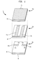
- FIG. 1 there is shown a perspective view of a filter for use in a microwave communications systems of the stripline type.
- the filter comprises a dielectric substrate 10 having three layers 10a, 10b, and 10c, wherein each structure is comprised of the inventive dielectric materials. Electrodes are incorporated into the layers of the substrate 10, including a pair of resonator electrodes 12a, 12b, disposed on the intermediate layer 10b, and coupling electrodes 14a, 14b, disposed on the bottom or end layer 10c. An earth electrode 16 covers substantially the entire outer circumference of the dielectric substrate 10.
- the coupling electrodes 14a, 14b are connected by extensions 14c, 14d, to input and output contacts 18a, 18b.
- Figure 1 shows an exemplary microwave filter in which the dielectric material of this invention may be incorporated; however, it is to be understood the invention is not limited to use with the filter shown.
- the dielectric material may be used in bulk-type resonators or in other applications besides microwave communications systems.
- the inventive composite may be fabricated from starting materials comprising fine powders of CaCO 3 (99.94%), Nb 2 O 5 (99.9%) and Ta 2 O 5 (99-98%). The following method was used to prepare the dielectric material from these starting materials and particularly for the thirteen members of the series reported in Table 1, below, within the range where x of Ca 2 Ta 2-x Nb x O 7 is from 0.00 to 2.00.
- the proportion of starting materials was changed, i.e., with larger amounts of Nb 2 O 5 for higher values of x and larger amounts of Ta 2 O 5 for lower values of x.
- the powders were mechanically ground and fired in Al 2 O 3 crucibles for 16 hours at 1350 °C in air.
- the powders were then ground in a ball mill (using zirconia balls) for 4 hours, filtered, dried, and pressed into disks about 1/2 inch in diameter and 0.125 inches in thickness. These disks were then fired in air for 2 to 3 hours at temperatures ranging from 1550 to 1425 °C, with the firing time and temperature variable with different values for x.
- the surfaces of the disks were sand smoothed, and electrical contact was made to the polycrystalline ceramic disks by applying 1:1 mole ratio Ga:In alloy solder electrodes.
- the materials were characterized by conventional powder X-ray diffraction.
- the dielectric constants reported in Table 1 were found to be independent of frequency in the 100KHz to 10MHz range for all materials at all temperatures studied. Small variations were noted but these were attributable to the lead wires and sample cells of the measurement circuit which caused small impedance imbalances.
- Table 1 when x was 0 (i.e., the material comprised Ca 2 Ta 2 O 7 ), the material exhibited a TCK of about -444 ppm/°C, and where x was 2.0 (i.e., the material comprised Ca 2 Nb 2 O 7 ), the material exhibited a TCK of about +231 ppm/°C.
- the dielectric constant was about 25.
- the dielectric constants for the mixtures are enhanced as compared with the pure end members.
- FIG. 3 plots the TCKs for the thirteen members of the series as a function of x, thus illustrating the variation in TCK with composition across the series.
- the materials are of the high Ca 2 Ta 2 O 7 type
- materials are of the Ca 2 Nb 2 O 7 -type solid solution.
- the materials unexpectedly are a mixture of the high Ca 2 Ta 2 O 7 type solid solution and a new phase, as further explained below.
- FIG. 4 plots the relative change in dielectric constant at 1 MHz for compositions Ca 2 Ta 2-x Nb x O 7 in the vicinity of the zero crossing of TCK.
- the changes in dielectric constant are plotted as percent deviations from the K value at 40 degrees C.
- a new phase is present in this system between the compositions x ⁇ 0.36 and x ⁇ 0.40, the diffraction pattern of which is subtly different from the Ca 2 Nb 2 O 7 type phase present when x is between approximately 0.5 and 2.0.
- the balance of the (small positive) TCK of that phase with the negative TCK of the Ca 2 Ta 2 O 7 phase yields good dielectric properties in this system.
Landscapes
- Engineering & Computer Science (AREA)
- Chemical & Material Sciences (AREA)
- Ceramic Engineering (AREA)
- Manufacturing & Machinery (AREA)
- Materials Engineering (AREA)
- Structural Engineering (AREA)
- Organic Chemistry (AREA)
- Inorganic Insulating Materials (AREA)
- Compositions Of Oxide Ceramics (AREA)
- Control Of Motors That Do Not Use Commutators (AREA)
Applications Claiming Priority (2)
| Application Number | Priority Date | Filing Date | Title |
|---|---|---|---|
| US971422 | 1992-11-03 | ||
| US08/971,422 US5993947A (en) | 1997-11-17 | 1997-11-17 | Low temperature coefficient dielectric material comprising binary calcium niobate and calcium tantalate oxides |
Publications (2)
| Publication Number | Publication Date |
|---|---|
| EP0916632A2 true EP0916632A2 (de) | 1999-05-19 |
| EP0916632A3 EP0916632A3 (de) | 1999-06-02 |
Family
ID=25518367
Family Applications (1)
| Application Number | Title | Priority Date | Filing Date |
|---|---|---|---|
| EP98309193A Withdrawn EP0916632A3 (de) | 1997-11-17 | 1998-11-10 | Binäre Oxide von Calciumniobat und Calciumtantalat enthaltendes dielektrisches Material mit niedrigem Temperaturkoeffizienten |
Country Status (3)
| Country | Link |
|---|---|
| US (1) | US5993947A (de) |
| EP (1) | EP0916632A3 (de) |
| JP (1) | JPH11260149A (de) |
Cited By (3)
| Publication number | Priority date | Publication date | Assignee | Title |
|---|---|---|---|---|
| WO2002018295A1 (de) * | 2000-08-29 | 2002-03-07 | Epcos Ag | Verfahren zur herstellung eines keramischen silber niobium tantalat körpers |
| WO2002019462A1 (de) * | 2000-08-29 | 2002-03-07 | Epcos Ag | Mikrowellen-bauelement mit einem silber niobium tantalat enthaltenden dielektrischen keramischen grundkörper |
| WO2002018294A1 (de) * | 2000-08-29 | 2002-03-07 | Epcos Ag | Ein silber niobium tantalat enthaltendes dielektrisches keramikmaterial |
Families Citing this family (5)
| Publication number | Priority date | Publication date | Assignee | Title |
|---|---|---|---|---|
| JP3578673B2 (ja) | 1999-08-05 | 2004-10-20 | 松下電器産業株式会社 | 誘電体積層フィルタおよびその製造方法 |
| US6495474B1 (en) | 2000-09-11 | 2002-12-17 | Agere Systems Inc. | Method of fabricating a dielectric layer |
| US7347983B2 (en) * | 2003-03-31 | 2008-03-25 | Council Of Scientific & Industrial Research | Mg2MM'o 6+x, (M=Y, rare earth metal and M'=SN, OR Zr) dielectric ceramics |
| CN111825446B (zh) * | 2020-07-03 | 2022-08-12 | 成都宏科电子科技有限公司 | 一种bt-brt复合超低损耗多层瓷介电容器用介质陶瓷材料及其制备方法和应用 |
| CN116751056B (zh) * | 2023-06-14 | 2024-06-25 | 云南贵金属实验室有限公司 | 一种二氧化钛掺杂铌酸钙陶瓷材料及其制备方法和应用 |
Family Cites Families (8)
| Publication number | Priority date | Publication date | Assignee | Title |
|---|---|---|---|---|
| JPS5829255B2 (ja) * | 1974-04-05 | 1983-06-21 | 日本電気株式会社 | サンカブツユウデンザイリヨウ |
| JPS51149598A (en) * | 1975-02-24 | 1976-12-22 | Nec Corp | Piezoelectric body material |
| US4131479A (en) * | 1976-03-08 | 1978-12-26 | Tokyo Shibaura Electric Co., Ltd. | Transparent ceramics |
| JPS5951090B2 (ja) * | 1979-05-17 | 1984-12-12 | 松下電器産業株式会社 | 誘電体磁器材料 |
| US4542083A (en) * | 1982-06-01 | 1985-09-17 | At&T Bell Laboratories | Nonaqueous cell using mixed metal oxide positive electrode |
| US4675302A (en) * | 1984-06-01 | 1987-06-23 | The Perkin-Elmer Corporation | Low expansion ceramic material |
| DE3850800T2 (de) * | 1987-04-13 | 1994-11-17 | Hitachi Ltd | Supraleitendes Material und Verfahren zu dessen Herstellung. |
| JPH06196031A (ja) * | 1992-12-22 | 1994-07-15 | Natl Res Inst For Metals | 酸化物超電導線材の製造方法 |
-
1997
- 1997-11-17 US US08/971,422 patent/US5993947A/en not_active Expired - Lifetime
-
1998
- 1998-11-10 EP EP98309193A patent/EP0916632A3/de not_active Withdrawn
- 1998-11-17 JP JP10325752A patent/JPH11260149A/ja active Pending
Non-Patent Citations (4)
| Title |
|---|
| DATABASE WPI Week 7706 Derwent Publications Ltd., London, GB; AN 77-10188y XP002098981 & JP 51 149598 A (NIPPON ELECTRIC CO.) , 21 December 1976 * |
| DATABASE WPI Week 8106 Derwent Publications Ltd., London, GB; AN 81-08529d XP002098982 & JP 55 154004 A (MATSUSHITA ELECTRIC IND. CO. LTD.), 1 December 1980 * |
| DATABASE WPI Week 8328 Derwent Publications Ltd., London, GB; AN 83-709347 XP002098980 & JP 50 131695 A (NIPPON ELECTRIC CO.) , 17 October 1975 * |
| R. CAVA ET AL.: MATERIALS RESEARCH BULLETIN, vol. 33, no. 04, 1998, pages 527-532, XP004127688 * |
Cited By (5)
| Publication number | Priority date | Publication date | Assignee | Title |
|---|---|---|---|---|
| WO2002018295A1 (de) * | 2000-08-29 | 2002-03-07 | Epcos Ag | Verfahren zur herstellung eines keramischen silber niobium tantalat körpers |
| WO2002019462A1 (de) * | 2000-08-29 | 2002-03-07 | Epcos Ag | Mikrowellen-bauelement mit einem silber niobium tantalat enthaltenden dielektrischen keramischen grundkörper |
| WO2002018294A1 (de) * | 2000-08-29 | 2002-03-07 | Epcos Ag | Ein silber niobium tantalat enthaltendes dielektrisches keramikmaterial |
| US6843956B2 (en) | 2000-08-29 | 2005-01-18 | Epcos Ag | Method for producing a ceramic silver niobium tantalate body |
| US6956001B2 (en) | 2000-08-29 | 2005-10-18 | Epcos Ag | Dielectric Ceramic Material |
Also Published As
| Publication number | Publication date |
|---|---|
| US5993947A (en) | 1999-11-30 |
| EP0916632A3 (de) | 1999-06-02 |
| JPH11260149A (ja) | 1999-09-24 |
Similar Documents
| Publication | Publication Date | Title |
|---|---|---|
| JP3482394B2 (ja) | 圧電磁器組成物 | |
| KR100282598B1 (ko) | 압전 세라믹 조성물 | |
| US20030181312A1 (en) | Microwave dielectric ceramic composition of the formula xMO-yLa2O3-zTiO2 (M= Sr, Ca; x:y:z = 1:2:4, 2:2:5, 1:2:5 or 1:4:9), method of manufacture thereof and devices comprising the same | |
| US6936559B2 (en) | Tunable devices incorporating cacu3ti4o12 | |
| US5993947A (en) | Low temperature coefficient dielectric material comprising binary calcium niobate and calcium tantalate oxides | |
| JPH11228225A (ja) | 圧電磁器組成物 | |
| US5256639A (en) | Dielectric ceramic composition | |
| US5459115A (en) | Composition of dielectric ceramics | |
| JPH0527202B2 (de) | ||
| EP0625491B1 (de) | Dielektrische keramische Zusammensetzung für Gebrauch in Hochfrequenzbereich | |
| JP3113829B2 (ja) | 誘電体磁器造成物 | |
| JP2881424B2 (ja) | 圧電磁器 | |
| JP4303369B2 (ja) | 誘電体磁器組成物及びこれを用いた誘電体共振器 | |
| US6093668A (en) | Low temperature coefficient dielectric materials and devices comprising same | |
| US5569632A (en) | Compositions of high frequency dielectrics | |
| JPH0840769A (ja) | 高周波用誘電体材料 | |
| JP2579139B2 (ja) | 高周波用誘電体組成物 | |
| JP3605295B2 (ja) | 誘電体磁器組成物及びこれを用いた誘電体共振器 | |
| JP4467168B2 (ja) | 圧電磁器および圧電素子 | |
| JPH067441B2 (ja) | 誘電体磁器組成物 | |
| EP0156312A2 (de) | Piezoelektrische keramische Masse für einen Resonator im elektrischen Wellenfilter | |
| JP2987762B2 (ja) | 強誘電体磁器組成物 | |
| JPH11100258A (ja) | 高周波用配線基板 | |
| JPS63182255A (ja) | 圧電磁器組成物 | |
| JP2932297B2 (ja) | 強誘電体磁器組成物 |
Legal Events
| Date | Code | Title | Description |
|---|---|---|---|
| PUAI | Public reference made under article 153(3) epc to a published international application that has entered the european phase |
Free format text: ORIGINAL CODE: 0009012 |
|
| PUAL | Search report despatched |
Free format text: ORIGINAL CODE: 0009013 |
|
| AK | Designated contracting states |
Kind code of ref document: A2 Designated state(s): DE FR GB |
|
| AX | Request for extension of the european patent |
Free format text: AL;LT;LV;MK;RO;SI |
|
| AK | Designated contracting states |
Kind code of ref document: A3 Designated state(s): AT BE CH CY DE DK ES FI FR GB GR IE IT LI LU MC NL PT SE |
|
| AX | Request for extension of the european patent |
Free format text: AL;LT;LV;MK;RO;SI |
|
| 17P | Request for examination filed |
Effective date: 19991119 |
|
| AKX | Designation fees paid |
Free format text: DE FR GB |
|
| 17Q | First examination report despatched |
Effective date: 20010926 |
|
| STAA | Information on the status of an ep patent application or granted ep patent |
Free format text: STATUS: THE APPLICATION IS DEEMED TO BE WITHDRAWN |
|
| 18D | Application deemed to be withdrawn |
Effective date: 20021228 |