EP0910171A1 - Frequency synthesizer - Google Patents
Frequency synthesizer Download PDFInfo
- Publication number
- EP0910171A1 EP0910171A1 EP98308488A EP98308488A EP0910171A1 EP 0910171 A1 EP0910171 A1 EP 0910171A1 EP 98308488 A EP98308488 A EP 98308488A EP 98308488 A EP98308488 A EP 98308488A EP 0910171 A1 EP0910171 A1 EP 0910171A1
- Authority
- EP
- European Patent Office
- Prior art keywords
- frequency
- signal
- oscillator
- capacitor
- aforementioned
- Prior art date
- Legal status (The legal status is an assumption and is not a legal conclusion. Google has not performed a legal analysis and makes no representation as to the accuracy of the status listed.)
- Withdrawn
Links
- 239000003990 capacitor Substances 0.000 claims abstract description 65
- 230000000052 comparative effect Effects 0.000 claims abstract description 17
- 230000005540 biological transmission Effects 0.000 claims description 8
- 230000000737 periodic effect Effects 0.000 claims description 2
- 238000010586 diagram Methods 0.000 description 7
- 230000001413 cellular effect Effects 0.000 description 4
- 238000005516 engineering process Methods 0.000 description 3
- 239000004065 semiconductor Substances 0.000 description 3
- 238000007599 discharging Methods 0.000 description 2
- 238000004891 communication Methods 0.000 description 1
- 230000006866 deterioration Effects 0.000 description 1
- 238000000034 method Methods 0.000 description 1
- 230000003287 optical effect Effects 0.000 description 1
Images


Classifications
-
- H—ELECTRICITY
- H03—ELECTRONIC CIRCUITRY
- H03L—AUTOMATIC CONTROL, STARTING, SYNCHRONISATION OR STABILISATION OF GENERATORS OF ELECTRONIC OSCILLATIONS OR PULSES
- H03L7/00—Automatic control of frequency or phase; Synchronisation
- H03L7/06—Automatic control of frequency or phase; Synchronisation using a reference signal applied to a frequency- or phase-locked loop
- H03L7/16—Indirect frequency synthesis, i.e. generating a desired one of a number of predetermined frequencies using a frequency- or phase-locked loop
- H03L7/18—Indirect frequency synthesis, i.e. generating a desired one of a number of predetermined frequencies using a frequency- or phase-locked loop using a frequency divider or counter in the loop
- H03L7/197—Indirect frequency synthesis, i.e. generating a desired one of a number of predetermined frequencies using a frequency- or phase-locked loop using a frequency divider or counter in the loop a time difference being used for locking the loop, the counter counting between numbers which are variable in time or the frequency divider dividing by a factor variable in time, e.g. for obtaining fractional frequency division
- H03L7/1974—Indirect frequency synthesis, i.e. generating a desired one of a number of predetermined frequencies using a frequency- or phase-locked loop using a frequency divider or counter in the loop a time difference being used for locking the loop, the counter counting between numbers which are variable in time or the frequency divider dividing by a factor variable in time, e.g. for obtaining fractional frequency division for fractional frequency division
-
- H—ELECTRICITY
- H03—ELECTRONIC CIRCUITRY
- H03L—AUTOMATIC CONTROL, STARTING, SYNCHRONISATION OR STABILISATION OF GENERATORS OF ELECTRONIC OSCILLATIONS OR PULSES
- H03L7/00—Automatic control of frequency or phase; Synchronisation
- H03L7/06—Automatic control of frequency or phase; Synchronisation using a reference signal applied to a frequency- or phase-locked loop
- H03L7/08—Details of the phase-locked loop
- H03L7/085—Details of the phase-locked loop concerning mainly the frequency- or phase-detection arrangement including the filtering or amplification of its output signal
- H03L7/089—Details of the phase-locked loop concerning mainly the frequency- or phase-detection arrangement including the filtering or amplification of its output signal the phase or frequency detector generating up-down pulses
- H03L7/0891—Details of the phase-locked loop concerning mainly the frequency- or phase-detection arrangement including the filtering or amplification of its output signal the phase or frequency detector generating up-down pulses the up-down pulses controlling source and sink current generators, e.g. a charge pump
Definitions
- the invention pertains to the technical field of frequency synthesizers.
- the invention pertains to a technology for ripple component compensation when the counter frequency division value is changed periodically.
- the cellular phone is of the frequency multi-channel access type.
- a frequency synthesizer which can lock on to an available channel at high speed.
- 101 represents an example of the frequency synthesizer of the prior art using the PLL circuit technology of the fractional frequency division method. It is arranged inside the semiconductor device that forms a transceiver of the cellular phone.
- This frequency synthesizer 101 contains the following parts: oscillator 131, frequency divider 132, reference clock signal generator 133, phase comparator 134, charge pump circuit 135, and low-pass filter 136.
- Said oscillator 131 has a configuration that outputs external signal OUT to the other circuit in the semiconductor device having frequency divider 132 and frequency synthesizer 101.
- Frequency divider 132 divides input external output signal OUT and generates a comparative signal.
- a comparative signal from frequency divider 132 and a reference clock signal output from reference clock generator 133 are input to phase comparator 134; the phase of the signals is read. The result is used as a control signal which is output through charge pump circuit 135 and low-pass filter 136 to oscillator 131.
- the frequency of external output signal OUT is changed such that the comparative signal and the reference clock signal are in phase.
- the frequency of external output signal OUT becomes a value equal to the frequency of the reference clock signal times the division value of frequency divider 132.
- the inter-channel distance is 25 kHz, 12.5 kHz, etc. Consequently, it is necessary to form external output signal OUT with narrow channel intervals, such as 800.025 MHz, 800.050 MHz, etc.
- the reference clock signal in order to increase the response speed, the reference clock signal must be a high frequency signal. Consequently, the frequency division value of frequency divider 132 is changed periodically, an average frequency division value having a fraction value is generated, and the high-frequency reference clock signal is multiplied by the average frequency division value, so that external output signal OUT having the desired frequency is obtained.
- phase comparator 134 a control signal indicating the phase difference between the comparative signal and the reference clock signal becomes a ripple current and is output through a charge pump circuit.
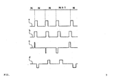
- (a) represents the waveform of the comparative signal output from frequency divider 132 in the case of frequency division of external output signal OUT to frequency division value N and frequency division value N+1.
- (b) represents the reference clock signal. Since it is not in agreement with the phase of comparative signal (a), ripple current c is superimposed on the control signal output from charge pump circuit 135.
- Such ripple current c not only degrades the receiving characteristics of the cellular phone or other communication device, but also acts as an interference component in transmission. Consequently, it becomes a serious problem.
- compensation circuit 140 made up of a charge pump circuit is arranged in frequency synthesizer 102 shown in FIG. 8. As shown by (d) in FIG. 7, compensation current having a polarity opposite to ripple current c is generated, ripple current c is cancelled by compensation current d, and the phase of external output signal OUT is locked. In this state, the signal that changes the frequency of external output signal OUT is not input to oscillator 131.
- compensation current d is output with a certain delay with respect to ripple current c. Also, the output time of compensation current d becomes longer than the output time of ripple current c. This is a disadvantage. For example, while the duration of output of ripple current c is as short as several hundred psec, the duration of compensation time d is several hundred nsec. Consequently, when ripple current c has a current value of a few mA, in order to provide the same charge amount but with opposite polarity, the current value of compensation current d becomes as small as a few ⁇ A, and it is impossible to perform the cancellation correctly. Consequently, it is difficult to eliminate the influence of ripple current c on conventional compensation circuit 140.
- FIG. 9 is a graph illustrating the relationship between the frequency component and optical intensity of output signal OUT of said frequency synthesizer 102.
- the abscissa represents intensity, and the ordinate frequency.
- the reference clock signal has a frequency of 240 kHz, and the average frequency division value is 4,000 + 1/8.
- a spurious component is observed at a prescribed frequency interval. Such spurious components cause deterioration in the transceiving characteristics, and it is preferred that such spurious components be eliminated.
- the purpose of the invention is to solve the aforementioned problems of the conventional technology by providing a type of frequency synthesizer which substantially eliminates spurious components in the output signal, and which has excellent characteristics.
- a type of frequency synthesizer that contains an oscillator which outputs an output signal to the outside, a frequency divider which divides the external output signal output from the aforementioned oscillator so that its frequency division value is in periodic variation to generate a comparative signal, a phase comparator which compares the phase of the aforementioned comparative signal with the phase of a reference clock signal, and controls the aforementioned oscillator such that the aforementioned external output signal has a frequency that equals the frequency of the aforementioned reference clock signal times the average frequency division value of the aforementioned frequency division values, a capacitor with one end connected to the transmission path of the signal that controls the aforementioned oscillator, and a voltage controller connected to the other end of the aforementioned capacitor.
- the aforementioned voltage controller can apply 2 or more voltages to the other end of each of the aforementioned capacitors.
- the aforementioned voltage controller of the frequency synthesizer may have two or more power sources and plural switch circuits that output different voltages; the aforementioned capacitors may be connected to two or more of the aforementioned power sources through the aforementioned switching circuits, respectively; and, by operating the aforementioned switching circuits, it is possible to switch the power source connected to the desired capacitor.
- the aforementioned voltage controller may comprise a digital/analog converter so configured that the desired voltage can be applied to the aforementioned capacitor.
- the frequency synthesizer described herein having the aforementioned configuration has an oscillator, a frequency divider, and a phase comparator.
- the frequency divider makes the frequency division value change periodically, and divides the external output signal output from the oscillator to generate a comparative signal.
- the phase comparator compares the phase of the comparative signal with the phase of the reference clock signal, and it controls the oscillator such that the external output signal has a frequency equal to the frequency of the reference clock signal times the average frequency division value.
- a capacitor and a voltage controller are used in this frequency synthesizer.
- One end of the capacitor is connected to the transmission path of the signal that controls the oscillator, and the other end is connected to the voltage controller.
- the charge amount of the ripple current is an integral multiple of the minimum charge amount. Consequently, plural capacitors are set, and, by means of a voltage controller, at least two voltages can be applied to the other end of each capacitor by means of the voltage controller. By switching the voltage of each capacitor, it is possible to generate the compensation current with the minimum charge amount. In this way, it is possible to cancel the ripple current correctly with a charge amount that is an integral multiple of the minimum charge amount.
- two or more power sources that can output different voltages and plural switch circuits are arranged in the voltage control circuit.
- the capacitors can be connected through the switching circuits to two more respective power sources.
- the voltage controller is made up of a digital/analog converter, and it can apply the desired voltage to the capacitor.
- the amount of change to the output voltage of the digital/analog converter it is possible to generate the compensating current having the desired charge amount.
- one capacitor may be sufficient for the operation.
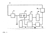
- 2 represents an example of a frequency synthesizer. It may be installed inside a semiconductor device.
- Said frequency synthesizer 2 has oscillator 31, frequency divider 32, reference clock signal 33, phase comparator 34, charge pump circuit 35, low-pass filter 36, controller 38, and compensation circuit 10.
- the external output signal OUT output from oscillator 31 is sent to the other circuits in the circuit, and it is also output to frequency divider 32.
- Said frequency divider 32 has a configuration which enables control by controller 38 and has the frequency division value change periodically. External output signal OUT that is input is divided by the frequency division value to generate a comparative signal at a lower frequency.
- Reference clock signal generator 33 generates the reference clock signal at the prescribed frequency, and the reference clock signal and the comparative signal are input to phase comparator 34.
- Phase comparator 34 compares the phases of the two signals, and outputs the comparison result as a control signal to charge pump circuit 35.
- Charge pump circuit 35 converts the control signal input from phase comparator 34 to a current (charge), and outputs it through low-pass filter 36 to oscillator 31.
- Oscillator 31 follows the input control signal to change the frequency of external output signal OUT. As a result, the frequency of external output signal OUT is locked to the value equal to frequency of the reference clock signal times the average frequency division value.
- the frequency division value of frequency divider 32 has an average frequency division value of N + 1/8.
- the reference clock signal is 200 kHz and said N is 5,000, external output signal OUT becomes a frequency of 1,000,025 kHz.
- the ripple current is contained in the control signal output from phase comparator 34.
- the output stage of said charge pump circuit 35 is made up of switch 44 and two constant-current circuits 41 and 42. Switch 44 is controlled by the control signal input from phase comparator 34.
- the charge calculated by multiplying the phase difference of the output current of constant-current circuits 41 and 42 (phase difference x constant current) is supplied or removed, so that the control signal is converted into charge. Consequently, the control signal input to oscillator 31 contains the charge ripple (current).
- low-pass filter 36 is made up of two capacitors and one resistor, and the capacitance of capacitor 36 1 , is less than the capacitance of capacitor 36 2 .
- the ripple charge generated becomes a charge amount in the range from a minimum value of ⁇ 0.5 times Qr ( ⁇ 0.5 Qr) to a maximm value of ⁇ 3.5 times Qr ( ⁇ 3.5 Qr) with interval of ⁇ 1.0 Qr.
- compensation circuit 10 is connected to the output terminal side of charge pump circuit 35.
- controller 38 the capacitor in compensating circuit 10 charges/discharges, so that a compensation current having charge polarity opposite to that of the ripple current and having charge amount equal to that of the ripple current is generated.
- Said compensation circuit 10 has plural capacitors 11 (here, three capacitors 111-113 are shown) and voltage controller 12.
- switch circuits 13 in equal number to the capacitors (here, three switch circuits 131-133 are shown) and two power sources 14 and 15 that output different voltages are arranged. One end of each capacitor 11 is connected to the output terminal of charge pump circuit 35, and the other end is connected through switch circuit 13 to power source 14 or 15.
- each capacitor 11 is connected to one of two power sources 14 and 15 beforehand.
- the connection state can be switched for the desired switch circuits, so that connection is switched to the other power source of said two power sources 14 and 15.
- the switching number of capacitors 11 can be represented as -7, -5, -3, -1, +1, +3, +5, +7.
- 3 represents an alternative frequency synthesizer configuration.
- Compensation circuit 10 of said frequency synthesizer 2 is changed to a different compensation circuit 20.
- the other structural features of said frequency synthesizer 3 are identical to those of said frequency synthesizer 2. Consequently, explanation of the overall operation is omitted.
- Compensation circuit 20 in FIG. 3 functions together with low-pass filter 36.
- D/A converter 24 and two resistors 22 and 23 are added.
- One end of capacitor 361 of low-pass filter 36 is connected to the output terminal of charge pump circuit 35, and the other end is connected through resistor 22 to the output terminal of D/A comparator 24.
- D/A converter 24 is controlled by controller 38.
- the digital signal input from controller 38 is converted into an analog voltage signal, and the voltage is applied to capacitor 361 via resistor 22.
- resistor 23 which has one end grounded, is connected to the node between capacitor 36 1 and resistor 22.
- capacitor 36 1 the capacitance of capacitor 36 1 is C 1 and the resistances of resistors 22 and 23 are R22 and R23, respectively, when the output voltage of D/A converter 24 is changed by V e , a compensation current with charge of C 1 • (R 23 /(R 22 + R 23 )) • V e is output from capacitor 361.
- C1 1,000 pF
- R22 is 99.9 k•
- R23 is 100 •
- Qr is 1.25 x 10⁻¹⁴ as described above
- V e is 6.35 mV.
- the ripple current makes change in the following order +3.5Q r ⁇ +2.5Q r ⁇ +1.5Q r ⁇ +0.5Q r ⁇ -0.5Q r ⁇ -1.5Q r ⁇ -2.5Q r ⁇ -3.5Q r Consequently, as shown in FIG. 4, at the moment that the ripple current is output, the output voltage of D/A comparator 24 is changed in the order of -7V e , -5V e , -3V e , -1V e , +1V e , +3V e , +5V e , +7V e .
Landscapes
- Stabilization Of Oscillater, Synchronisation, Frequency Synthesizers (AREA)
Applications Claiming Priority (2)
| Application Number | Priority Date | Filing Date | Title |
|---|---|---|---|
| JP29948297A JP3923150B2 (ja) | 1997-10-16 | 1997-10-16 | 周波数シンセサイザ |
| JP299482/97 | 1997-10-16 |
Publications (1)
| Publication Number | Publication Date |
|---|---|
| EP0910171A1 true EP0910171A1 (en) | 1999-04-21 |
Family
ID=17873150
Family Applications (1)
| Application Number | Title | Priority Date | Filing Date |
|---|---|---|---|
| EP98308488A Withdrawn EP0910171A1 (en) | 1997-10-16 | 1998-10-16 | Frequency synthesizer |
Country Status (3)
| Country | Link |
|---|---|
| US (1) | US6169457B1 (enExample) |
| EP (1) | EP0910171A1 (enExample) |
| JP (1) | JP3923150B2 (enExample) |
Cited By (1)
| Publication number | Priority date | Publication date | Assignee | Title |
|---|---|---|---|---|
| CN100403666C (zh) * | 2001-12-12 | 2008-07-16 | 爱立信股份有限公司 | 用于信号传输的方法和设备 |
Families Citing this family (14)
| Publication number | Priority date | Publication date | Assignee | Title |
|---|---|---|---|---|
| US6278331B1 (en) | 1999-03-30 | 2001-08-21 | Infineon Technologies Ag | System and method for compensating wafer parameters |
| JP4631120B2 (ja) | 2000-02-02 | 2011-02-16 | 日本テキサス・インスツルメンツ株式会社 | 周波数シンセサイザ、位相同期ループ周波数シンセサイザ |
| JP4392949B2 (ja) | 2000-04-05 | 2010-01-06 | 日本テキサス・インスツルメンツ株式会社 | 周波数シンセサイザ |
| US6891412B1 (en) * | 2002-12-16 | 2005-05-10 | Analog Devices, Inc. | Low noise filter |
| US7174143B1 (en) * | 2003-01-21 | 2007-02-06 | Analog Devices, Inc. | Receiver circuit with transmission loss compensation |
| US8193845B2 (en) | 2010-07-06 | 2012-06-05 | Microchip Technology Incorporated | Binary-weighted delta-sigma fractional-N frequency synthesizer with digital-to-analog differentiators canceling quantization noise |
| WO2012151466A2 (en) | 2011-05-05 | 2012-11-08 | Arctic Sand Technologies, Inc. | Dc-dc converter with modular stages |
| US10680515B2 (en) | 2011-05-05 | 2020-06-09 | Psemi Corporation | Power converters with modular stages |
| US8743553B2 (en) | 2011-10-18 | 2014-06-03 | Arctic Sand Technologies, Inc. | Power converters with integrated capacitors |
| US8619445B1 (en) | 2013-03-15 | 2013-12-31 | Arctic Sand Technologies, Inc. | Protection of switched capacitor power converter |
| US8724353B1 (en) | 2013-03-15 | 2014-05-13 | Arctic Sand Technologies, Inc. | Efficient gate drivers for switched capacitor converters |
| US9041459B2 (en) * | 2013-09-16 | 2015-05-26 | Arctic Sand Technologies, Inc. | Partial adiabatic conversion |
| WO2016149063A1 (en) | 2015-03-13 | 2016-09-22 | Arctic Sand Technologies, Inc. | Dc-dc transformer with inductor for the facilitation of adiabatic inter-capacitor charge transport |
| CN108028600B (zh) | 2015-07-08 | 2022-03-08 | 派更半导体公司 | 开关电容器电力转换器 |
Citations (4)
| Publication number | Priority date | Publication date | Assignee | Title |
|---|---|---|---|---|
| US4204174A (en) * | 1978-07-22 | 1980-05-20 | Racal Communications Equipment Limited | Phase locked loop variable frequency generator |
| EP0429217A2 (en) * | 1989-11-22 | 1991-05-29 | Nortel Networks Corporation | Frequency synthesiser |
| US5166642A (en) * | 1992-02-18 | 1992-11-24 | Motorola, Inc. | Multiple accumulator fractional N synthesis with series recombination |
| US5495206A (en) * | 1993-10-29 | 1996-02-27 | Motorola, Inc. | Fractional N frequency synthesis with residual error correction and method thereof |
Family Cites Families (4)
| Publication number | Priority date | Publication date | Assignee | Title |
|---|---|---|---|---|
| GB429217A (en) | 1934-03-21 | 1935-05-27 | Gen Electric Co Ltd | Improvements in or relating to radio receiving sets |
| JP2855628B2 (ja) * | 1988-05-11 | 1999-02-10 | セイコーエプソン株式会社 | 位相同期回路 |
| FR2689342A1 (fr) * | 1992-03-31 | 1993-10-01 | Sgs Thomson Microelectronics | Boucle à verrouillage de fréquence. |
| JP3647147B2 (ja) * | 1996-06-28 | 2005-05-11 | 富士通株式会社 | 発振回路とそれを利用したpll回路 |
-
1997
- 1997-10-16 JP JP29948297A patent/JP3923150B2/ja not_active Expired - Fee Related
-
1998
- 1998-10-13 US US09/170,458 patent/US6169457B1/en not_active Expired - Lifetime
- 1998-10-16 EP EP98308488A patent/EP0910171A1/en not_active Withdrawn
Patent Citations (4)
| Publication number | Priority date | Publication date | Assignee | Title |
|---|---|---|---|---|
| US4204174A (en) * | 1978-07-22 | 1980-05-20 | Racal Communications Equipment Limited | Phase locked loop variable frequency generator |
| EP0429217A2 (en) * | 1989-11-22 | 1991-05-29 | Nortel Networks Corporation | Frequency synthesiser |
| US5166642A (en) * | 1992-02-18 | 1992-11-24 | Motorola, Inc. | Multiple accumulator fractional N synthesis with series recombination |
| US5495206A (en) * | 1993-10-29 | 1996-02-27 | Motorola, Inc. | Fractional N frequency synthesis with residual error correction and method thereof |
Cited By (1)
| Publication number | Priority date | Publication date | Assignee | Title |
|---|---|---|---|---|
| CN100403666C (zh) * | 2001-12-12 | 2008-07-16 | 爱立信股份有限公司 | 用于信号传输的方法和设备 |
Also Published As
| Publication number | Publication date |
|---|---|
| JPH11122106A (ja) | 1999-04-30 |
| US6169457B1 (en) | 2001-01-02 |
| JP3923150B2 (ja) | 2007-05-30 |
Similar Documents
| Publication | Publication Date | Title |
|---|---|---|
| EP0910171A1 (en) | Frequency synthesizer | |
| US6559698B1 (en) | Spread spectrum type clock generating circuit | |
| US8437441B2 (en) | Phase locked loop capable of fast locking | |
| CN1158768C (zh) | 带有抖动补偿的分数n分频的频率综合器 | |
| EP0211594B1 (en) | Phase-locked digital synthesiser | |
| EP0727877B1 (en) | Fast frequency switching synthesizer | |
| GB2431531A (en) | Triangle waveform generator for a PWM amplifier | |
| US7498888B2 (en) | Method and arrangement for interference compensation in a voltage-controlled frequency generator | |
| US4506233A (en) | Bandwidth control circuit for a phase locked loop | |
| US5150082A (en) | Center frequency calibration for DC coupled frequency modulation in a phase-locked loop | |
| KR20040007473A (ko) | 분수 보상방법을 갖는 분수분주 주파수 합성기 | |
| US6593783B2 (en) | Compensation circuit for fractional-N frequency PLL synthesizer | |
| EP1689088B1 (en) | Spread spectrum clock generation circuit and a method of controlling thereof | |
| JP4357674B2 (ja) | 周波数シンセサイザ | |
| US6766154B2 (en) | Fast settling fine stepping phase locked loops | |
| KR20050007821A (ko) | 적응적 가변 대역폭을 갖는 위상 동기 루프 회로 | |
| JP3895028B2 (ja) | 周波数シンセサイザ | |
| US20030076177A1 (en) | Phase locked loop with charge injection cancellation | |
| KR100932252B1 (ko) | 광수신 장치, 시험 장치, 광수신 방법, 시험 방법, 테스트모듈, 및 반도체 칩 | |
| AU705852B2 (en) | Clock and data regenerator for gigabit signals | |
| US6344813B1 (en) | Digital to analogue converter | |
| JP2001292061A (ja) | 周波数シンセサイザ | |
| JP3901810B2 (ja) | 補正回路付き周波数シンセサイザ | |
| US6912246B1 (en) | Clock signal transmitting system, digital signal transmitting system, clock signal transmitting method, and digital signal transmitting method | |
| JPH0267821A (ja) | 周波数シンセサイザ |
Legal Events
| Date | Code | Title | Description |
|---|---|---|---|
| PUAI | Public reference made under article 153(3) epc to a published international application that has entered the european phase |
Free format text: ORIGINAL CODE: 0009012 |
|
| AK | Designated contracting states |
Kind code of ref document: A1 Designated state(s): DE FR GB IT NL |
|
| AX | Request for extension of the european patent |
Free format text: AL;LT;LV;MK;RO;SI |
|
| 17P | Request for examination filed |
Effective date: 19991021 |
|
| AKX | Designation fees paid |
Free format text: DE FR GB IT NL |
|
| 17Q | First examination report despatched |
Effective date: 20020814 |
|
| STAA | Information on the status of an ep patent application or granted ep patent |
Free format text: STATUS: THE APPLICATION IS DEEMED TO BE WITHDRAWN |
|
| 18D | Application deemed to be withdrawn |
Effective date: 20030225 |