US7498888B2 - Method and arrangement for interference compensation in a voltage-controlled frequency generator - Google Patents
Method and arrangement for interference compensation in a voltage-controlled frequency generator Download PDFInfo
- Publication number
- US7498888B2 US7498888B2 US10/596,454 US59645404A US7498888B2 US 7498888 B2 US7498888 B2 US 7498888B2 US 59645404 A US59645404 A US 59645404A US 7498888 B2 US7498888 B2 US 7498888B2
- Authority
- US
- United States
- Prior art keywords
- voltage
- interference
- input
- resistor
- arrangement
- Prior art date
- Legal status (The legal status is an assumption and is not a legal conclusion. Google has not performed a legal analysis and makes no representation as to the accuracy of the status listed.)
- Active, expires
Links
Images


Classifications
-
- H—ELECTRICITY
- H03—ELECTRONIC CIRCUITRY
- H03L—AUTOMATIC CONTROL, STARTING, SYNCHRONISATION, OR STABILISATION OF GENERATORS OF ELECTRONIC OSCILLATIONS OR PULSES
- H03L7/00—Automatic control of frequency or phase; Synchronisation
- H03L7/06—Automatic control of frequency or phase; Synchronisation using a reference signal applied to a frequency- or phase-locked loop
- H03L7/16—Indirect frequency synthesis, i.e. generating a desired one of a number of predetermined frequencies using a frequency- or phase-locked loop
- H03L7/18—Indirect frequency synthesis, i.e. generating a desired one of a number of predetermined frequencies using a frequency- or phase-locked loop using a frequency divider or counter in the loop
-
- H—ELECTRICITY
- H03—ELECTRONIC CIRCUITRY
- H03L—AUTOMATIC CONTROL, STARTING, SYNCHRONISATION, OR STABILISATION OF GENERATORS OF ELECTRONIC OSCILLATIONS OR PULSES
- H03L7/00—Automatic control of frequency or phase; Synchronisation
- H03L7/06—Automatic control of frequency or phase; Synchronisation using a reference signal applied to a frequency- or phase-locked loop
- H03L7/08—Details of the phase-locked loop
- H03L7/085—Details of the phase-locked loop concerning mainly the frequency- or phase-detection arrangement including the filtering or amplification of its output signal
- H03L7/093—Details of the phase-locked loop concerning mainly the frequency- or phase-detection arrangement including the filtering or amplification of its output signal using special filtering or amplification characteristics in the loop
-
- H—ELECTRICITY
- H03—ELECTRONIC CIRCUITRY
- H03L—AUTOMATIC CONTROL, STARTING, SYNCHRONISATION, OR STABILISATION OF GENERATORS OF ELECTRONIC OSCILLATIONS OR PULSES
- H03L2207/00—Indexing scheme relating to automatic control of frequency or phase and to synchronisation
- H03L2207/06—Phase locked loops with a controlled oscillator having at least two frequency control terminals
Definitions
- the invention relates to a method and an arrangement for interference compensation in a voltage-controlled frequency generator, wherein the frequency generator is tuned to a nominal frequency via a tuning voltage V tune and whose actual frequency is compared with a reference frequency by means of a frequency comparison and is tuned if a deviation is discovered via the frequency comparison in which method in the event of interference the tuning voltage V tune is changed by an interference voltage V stör that depends on the interference event and thus a frequency deviating from the nominal frequency is generated, which deviating frequency is corrected again by the phase-locked loop.
- a desired carrier frequency is tuned to a desired value by means of a phase-locked loop (PLL). If it functions properly, a very stable carrier frequency is created by the phase-locked loop. This is used, in particular, for higher-order types of modulation, such as in WLAN systems with high transmission rates.
- PLL phase-locked loop
- the permissible static frequency deviation may be approx. 20 ppm, whereas it only takes a dynamic deviation of more than 0.5 ppm (2.5 kHz in the case of a 5 GHz carrier frequency) to bring about a reduction in performance.
- Modem communication standards typically require high-speed switching between reception and transmission, which may lead to short-term instability in the frequency of the phase-locked loop during and/or after a switching operation.
- the phase-locked loop exhibits a frequency that deviates from the predetermined desired value following a switching event that generates interference, which event may be switching to another possible channel i.e. the phase-locked loop is disengaged.
- the phase-locked loop adjusts the frequency of the voltage-controlled oscillator (VCO) until the nominal frequency value is reached; the phase-locked loop is thus re-engaged to the nominal frequency.
- the tuning voltage of the voltage-controlled oscillator V tune is then slightly different from the tuning voltage prior to the switching event or interference due to effects which lie outside the scope of this description.
- each interference event causes a transient response in the phase-locked loop, i.e. it determines the voltage step that has to be added to the tuning voltage V tune to compensate fully for the frequency deviation caused by the interference and, thus, to cause the phase-locked loop back to build up to the nominal frequency.
- a state-of-the-art phase-locked loop comprises, for example, a Phase Detector Charge Pump (PDCP) to which a reference clock pulse is fed.
- PDCP Phase Detector Charge Pump
- This module is connected to the Voltage-Controlled Oscillator (VCO) via a loop filter, possibly a third-order loop filter.
- VCO Voltage-Controlled Oscillator
- An output of the voltage-controlled oscillator which outputs the oscillator frequency is connected via a frequency divider to a second input of the phase detector charge pump for the purpose of comparing the nominal and actual frequencies. If the output frequency of the voltage-controlled oscillator deviates from a predefined nominal value, the control voltage of the voltage-controlled oscillator V tune is re-adjusted by the phase detector charge pump until the nominal frequency is reached.
- Known interference events are understood to mean state changes caused by the way in which the arrangement works, such as switching between a transmit and receive operation and vice versa, or a change of channel.
- the object of the invention is to create a method and an arrangement for interference compensation in a voltage-controlled frequency generator, thereby avoiding a deviation from a defined nominal frequency when known interference events occur.
- the object is achieved in accordance with the invention with a method for interference compensation in a phase-locked loop comprising a voltage-controlled frequency generator of the type mentioned in the opening paragraph so that, if a known interference event occurs, a voltage V comp which compensates for the interference voltage V stör is generated in synchronism with this with sign inversion and is superimposed on the interference voltage V stör .
- a switching operation from one state to another in a transmit/receive arrangement leads to a known interference event, and thus a change of the tuning voltage V tune which controls the voltage-controlled oscillator, by the amplitude value of the interference voltage V stör .
- V tune which controls the voltage-controlled oscillator
- V comp time-synchronous sign-inverted compensation voltage
- the relevant compensation voltage V comp is determined in one measuring operation for all possible known interference events, and this relevant voltage is stored in a compensation table.
- the measuring operation and the storing of the voltage values in the compensation table is effected when the arrangement is made operative and/or during operation.
- the interference voltage value V stör generated by an interference event must be known to facilitate the interference compensation in accordance with the invention
- the interference voltage value must be measured for each possible interference event, and the measured value must be stored in a database, for example in tabular form in a compensation table as a compensation voltage value.
- a succession of interference events known one after the other are simulated in one measuring operation by means of state changes in the transmit/receive unit, and measurements are performed. When an arrangement is made operative for the first time, this operation can be started periodically, program-controlled or through state changes during operation.
- the values stored in the table are used by the method in accordance with the invention to compensate for the interference.
- the measurement can also be performed during the interference compensation in accordance with the method in order to monitor how the method works and, in the event of compensation not taking place properly, to correct the value assigned to the interference event.
- the relevant compensation voltage value which is stored in the compensation table is read out before the occurrence of a known interference event generating interference voltage V stör , and with this value the generation of the compensation voltage V comp is controlled in synchronism with the occurrence of the interference voltage.
- the relevant value can be read from the compensation table in good time before the known interference event occurs and, with this value, the generation of the compensation voltage V comp can be controlled in synchronism with the interference event by means of a controllable voltage source, for example.
- the object is achieved in accordance with the invention in the case of an arrangement for interference compensation in a phase-locked loop including a voltage-controlled frequency generator of the type mentioned in the opening paragraph in such a way that the VarGND terminal for the voltage-controlled frequency generator is connected to a controllable voltage source.
- a compensation voltage V comp whose polarity is the reverse to that of the interference voltage V stör , is applied to the VarGND terminal, which is connected to the GND potential in the state of the art. If both voltages have the same amplitude value, they cancel each other out and thus their effect on the voltage-controlled frequency generator.
- controllable voltage source comprises a resistor located between the VarGND terminal and the GND potential and a current source connected between the VarGND terminal and the resistor.
- a current is driven through the resistor between the VarGND terminal and the GND potential by a controllable current source.
- the current causes a voltage drop to occur across the resistor. This voltage drop corresponds to the compensation voltage to be generated.
- the magnitude of the current generated by the controllable current source is determined by the compensation value which is read out from the compensation table beforehand.
- the VarGND terminal on the voltage-controlled frequency generator is connected to a digital-to-analog converter which generates a compensation current, and the digital-to-analog converter is connected to two registers via a transmit/receive switch.
- the VarGND terminal is connected to a controllable current source whose current flows through the resistor which is located between the VarGND terminal and the GND potential, thereby causing a voltage drop to occur across this resistor, which corresponds to the compensation voltage.
- the controllable current source which is designed as a digital-to-analog converter, is connected by a reversing switch either to a part of the register that governs transmission or to a part that governs reception, in which part the compensation values to be generated are stored.
- the VarGND terminal is connected to the controllable voltage source via a voltage divider in such a way that the voltage divider is connected with a first partial resistor to the controllable voltage source, and the second series-connected partial resistor is connected to the GND potential and the VarGND terminal is connected with the connection of the first partial resistor to the second partial resistor.
- a voltage source comprising a voltage divider with two resistors, to whose mid tap the VarGND terminal is connected, can be used to generate the compensation voltage V comp at the VarGND terminal of the controllable oscillator. Due to the dividing ratio of the voltage divider, the required compensation voltage V comp can be dimensioned accordingly. The voltage drop generated across the resistor between the VarGND terminal and GND corresponds to the compensation voltage V comp .
- the voltage source is controlled by the value stored in the compensation table and thus generates a voltage value that corresponds to the interference event.
- a phase detector charge pump is arranged to which a reference clock pulse is fed via the first phase detector input (PDin 1 ), wherein the output of the phase detector charge pump (Cpout) is connected to the input of a voltage-controlled frequency generator via a loop filter, that the output of the voltage-controlled frequency generator is connected to a second phase detector input (PDin 2 ) via a frequency divider, that furthermore a measuring circuit is arranged, and that the loop filter comprises a first capacitor at the input, a third capacitor at the output, a second resistor arranged between the input and the output of the loop filter and a series circuit which is connected to the input and comprises a first resistor and a second capacitor, while the second capacitor in the series circuit is connected to the input of the measuring circuit, the input of the measuring circuit forming a virtual ground terminal.
- a measuring device is configured in the arrangement, which device is connected to a terminal of the loop filter.
- the tuning voltage V tune is measured by this arrangement at different definable points in time. If, for example, a first measurement takes place before an interference event occurs and a second measurement is performed following the elapse of a defined time t, the voltage difference caused by the interference event can be measured, converted into a digital value and stored in the compensation table.
- the measuring circuit input forms a virtual ground terminal for the series circuit, which comprises a first resistor and a second capacitor, and leads to a slight deviation in potential from the real GND potential. However, this slight deviation has no functional influence on the functioning of the phase-locked loop.
- the measuring circuit comprises a negative-feedback inverting operational amplifier arrangement and an analog-to-digital converter unit.
- the voltage differences are amplified by an operational amplifier upstream of the analog-to-digital converter.
- the operational amplifier has an outer circuit comprising two negative-feedback anti-parallel diodes, which limit the voltage output to the downstream analog-to-digital converter to the range from 0V to 1.5V.
- a measuring circuit is connected to the V tune input of the voltage-controlled frequency generator, that the measuring circuit comprises a first operational amplifier which works as a buffer amplifier whose output is connected via a first resistor and a capacitor to the inverting input of a second operational amplifier working as a negative-feedback inverting amplifier, that the non-inverting input of the second operational amplifier is connected to a reference voltage, that the output of the second operational amplifier is fed back to the inverting input via two anti-parallel diodes, that the output of the second operational amplifier is further connected via a second resistor to the connection of the first resistor and the capacitor, and that the output of the second operational amplifier has a TDet terminal for outputting a voltage.
- Capacitors with higher capacitance values are problematic when incorporating the measuring circuit into an electric circuit.
- a solution is then, for example, to implement the capacitor as a non-desired, external component.
- the operational amplifier OP-AMP which is additionally required and whose non-inverting input is connected to the V tune terminal, works as a buffer amplifier.
- the second OP-AMP is operated as a negative-feedback inverting amplifier.
- the anti-parallel diodes in the negative feedback amplifier provide that the capacitor C is charged to such a voltage that the output signal TDet is limited to the range from 0 V to 1.5 V.
- FIG. 1 shows an arrangement of a phase-locked loop in accordance with the state of the art
- FIG. 2 shows an arrangement of a phase-locked loop with the interference voltage compensation in accordance with the invention
- FIG. 3 shows a typical flow chart of a transmitter/receiver unit
- FIG. 4 shows an arrangement of a phase-locked loop with the interference voltage compensation in accordance with the invention and a measuring arrangement for determining the interference voltage V stör ,
- FIG. 5 shows a further arrangement for implementing the compensation and measuring method in accordance with the invention in a transmitter/receiver unit
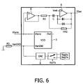
- FIG. 6 shows a further embodiment for implementing the method according to the invention, which is suitable for integration in an electric circuit.
- FIG. 1 shows an arrangement of a phase-locked loop as known from the state of the art. It comprises a phase detector charge pump 1 which is connected to a voltage-controlled oscillator (VCO) 3 via a third-order loop filter 2 comprising the elements R 1 , R 2 , C 1 , C 2 and C 3 . In order to regulate the frequency produced by the oscillator 3 at the output Out, this frequency is fed back to the input PDin 2 of the phase detector charge pump 1 via a frequency divider 4 . An external reference frequency is applied to the second input PDin 1 for the purposes of a frequency comparison.
- VCO voltage-controlled oscillator
- the tuning voltage V tune which regulates the oscillator frequency is changed until the nominal frequency value is achieved.
- a capacitor C 3 which belongs to the loop filter 2 , is connected in parallel to the input of the voltage-controlled oscillator 3 , so that one end of the capacitor C 3 is connected to the V tune input and the other end is connected to the VarGND terminal of the oscillator 3 .
- the VarGND terminal is further connected to the central GND potential of the circuit.
- the VarGND input of the oscillator 3 is, as shown in FIG. 2 , connected to the GND potential in the circuit via a third resistor R 3 .
- the voltage drop generated via this resistor corresponds to the compensation voltage V comp .
- Its amplitude can be controlled by a digital-to-analog converter 5 (DAC), which is connected to the input VarGND on the oscillator 3 and which generates a voltage or a current.
- DAC digital-to-analog converter 5
- a fourth resistor R 4 is inserted between the converter 5 and the input VarGND of the oscillator 3 .
- the required compensation voltage V comp is also small.
- FIG. 3 shows a typical process in a transmitter/receiver unit, in which the system is switched from a transmission state “Tx” to “CCA” state with a defined high reception gain.
- the AGC operation subsequently starts, followed by the actual reception operation “Rx”.
- Interference always occurs during transition from one operating state to a next, which interference is compensated for by the method in accordance with the invention, through the generation of a compensation voltage V comp associated with the interference.
- the relevant interference voltage V stör has to be determined. This necessitates a method and an arrangement for measuring the interference voltage V stör in the definitive system. A possible embodiment is shown in FIG. 4 .
- This measuring method should preferably not disrupt the normal function because, for example, drifting operating parameters due to temperature changes or other influences must be tracked.
- the difference in the tuning voltage V tune can be used both before and after the control time of the phase-locked loop as a measure or as an error criterion for the compensation values.
- V tune There should ideally be no change observed in the tuning voltage V tune during transition from one state to another if compensation has taken place properly.
- the difference in V tune values measured before the interference event and after the transient response by the phase-locked loop is in proportion to the interference voltage which occurs if the constants for each measurement remain unchanged.
- a suitable measuring circuit is shown in FIG. 4 where C 2 is connected to a virtual ground terminal, which is generated by an inverting operational amplifier 6 .
- the operational amplifier 6 should be a CMOS rail-to-rail type which can work up to the operating voltage limit for inputs and outputs and has small input currents.
- a floating DC voltage cap is limited by the anti-parallel diodes.
- the compensation voltage V comp is measured by calculating the difference between 2 ADC samples of the analog-to-digital converter unit 7 , while the first sample is determined close to the time of the interference event, and the second sample is determined following a transient response by the phase-locked loop, which is identified by the loop filter 2 .
- This difference is proportional to the voltage difference at C 1 , which is close to the difference of V tune if the low-pass filter, which is formed by R 2 and C 3 , has an essentially higher critical frequency than the main loop filter.
- the OP-AMP 6 is operated as a negative-feedback, inverting amplifier 6 , such as the type described in the book “ Analoge diche GmbH ” by Miklos Herpy (Franzis Verlag 1979, ISBN 3-7723-6152-8).
- This DC voltage which is additional to the original filter in FIG. 2 , is blocked by the capacitor C 2 and does not change the dynamic behavior.
- FIG. 5 shows a further variant of an arrangement in accordance with the invention for implementing the method in a TD- 2 RF structure.
- TD- 2 RF is based on superheterodyne architecture, always two phase-locked loops (IF und RF) are included in the transmission (Tx) and reception operation (Rx).
- Tx transmission
- Rx reception operation
- the circuit shown in FIG. 4 is configured twice in FIG. 5 .
- TD- 2 BB has 2 Sigma/Selta DACs which are used to compensate for the interference voltages.
- the TD 2 BB further supports an ADC for RSSI measurements, which ADC is connected to TD- 2 RF, while an analog multiplexer has two inputs which can be switched to the ADC via a simple differential converter.
- the loop filter 2 is designed in such a way that a complete transient response is achieved of the phase-locked loop within approx. 200 ⁇ s.
- changes can also be observed in the tuning voltage caused for example by a temperature drift, which changes also bring about changes to the tuning voltage V tune , without the phase-locked loop being broken.
- the ADC sample is generated about 100 ⁇ s after the change of state.
- An internal current mode DAC which is connected to the VarGND terminal, can be used for compensation, as FIG. 6 shows.
- This current mode DAC works as a controllable current source.
- An external resistor R 3 opposite the GND potential determines the effective compensation voltage. Based on experience with the TD- 2 RF, a 9-bit monotonous DAC with a 0.5 mA maximum output current to a 10 ohm external resistor should be used.
- the circuit shown in FIG. 4 generally requires capacitors which are too large for integration. However, it is sufficient for the circuit shown in FIG. 6 to have a capacitor C of the order of 1 pF and it is therefore more suitable for integration, although it requires a further operational amplifier OP-AMP 6 as a buffer amplifier. The latter is connected directly to the tuning voltage V tune , so that no additional IC pins are used other than those used in the conventional, uncompensated circuit.
- the anti-parallel diodes in the negative feedback mode provide that the capacitor C is charged to such a voltage that the output signal TDet is limited to the range from 0 to 1.5 V.
Abstract
Description
Z1=R1+1/(jωC2).
v=−Z2/Z1=−n
and is frequency-independent in particular. The behavior of the
- 1 Phase detector charge pump
- 2 Loop filter
- 3 Voltage-controlled frequency generator
- 4 Frequency divider
- 5 Digital-to-analog converter
- 6 Operational amplifier arrangement
- 7 Analog-to-digital converter unit
Claims (6)
Applications Claiming Priority (3)
| Application Number | Priority Date | Filing Date | Title |
|---|---|---|---|
| EP03104837.4 | 2003-12-19 | ||
| EP03104837 | 2003-12-19 | ||
| PCT/IB2004/052756 WO2005062471A1 (en) | 2003-12-19 | 2004-12-10 | Method and arrangement for interference compensation in a voltage-controlled frequency generator |
Publications (2)
| Publication Number | Publication Date |
|---|---|
| US20070194811A1 US20070194811A1 (en) | 2007-08-23 |
| US7498888B2 true US7498888B2 (en) | 2009-03-03 |
Family
ID=34707270
Family Applications (1)
| Application Number | Title | Priority Date | Filing Date |
|---|---|---|---|
| US10/596,454 Active 2025-10-27 US7498888B2 (en) | 2003-12-19 | 2004-12-10 | Method and arrangement for interference compensation in a voltage-controlled frequency generator |
Country Status (5)
| Country | Link |
|---|---|
| US (1) | US7498888B2 (en) |
| EP (1) | EP1698056A1 (en) |
| JP (1) | JP2007515120A (en) |
| CN (1) | CN1951016A (en) |
| WO (1) | WO2005062471A1 (en) |
Cited By (7)
| Publication number | Priority date | Publication date | Assignee | Title |
|---|---|---|---|---|
| US20080255907A1 (en) * | 2007-03-15 | 2008-10-16 | Ricoh Company, Ltd. | Class object wrappers for document object model (DOM) elements for project task management system for managing project schedules over a network |
| US20080297244A1 (en) * | 2007-05-29 | 2008-12-04 | Texas Instruments Incorporated | PWM Loop Filter with Minimum Aliasing Error |
| US20110102032A1 (en) * | 2009-10-29 | 2011-05-05 | Stmicroelectronics Design & Application Gmbh | Loop filter |
| US20110115535A1 (en) * | 2009-11-19 | 2011-05-19 | Electronics And Telecommunications Research Institute | Loop filter and phase locked loop including the same |
| EP2355362A2 (en) | 2010-02-05 | 2011-08-10 | Blue Wonder Communications GmbH | Rf transceiver and modem comprising such a transceiver |
| US20130027086A1 (en) * | 2011-07-26 | 2013-01-31 | United Microelectronics Corp. | Charge pump |
| US20140132321A1 (en) * | 2012-11-13 | 2014-05-15 | International Business Machines Corporation | Implementing compact current mode logic (cml) inductor capacitor (lc) voltage controlled oscillator (vco) for high-speed data communications |
Families Citing this family (12)
| Publication number | Priority date | Publication date | Assignee | Title |
|---|---|---|---|---|
| CN102467091B (en) * | 2010-11-11 | 2017-03-01 | 帝斯贝思数字信号处理和控制工程有限公司 | There is battery simulator and the method for fault simulation |
| CN102185663B (en) * | 2011-02-16 | 2014-07-30 | 意法·爱立信半导体(北京)有限公司 | Frequency calibration method and device |
| WO2012122695A1 (en) * | 2011-03-11 | 2012-09-20 | 海尔集团公司 | Wireless power supply device and method |
| US8611842B2 (en) * | 2011-11-04 | 2013-12-17 | Broadcom Corporation | Apparatus and method for fast phase locked loop (PLL) settling for cellular time-division duplex (TDD) communications systems |
| US9071253B2 (en) | 2011-11-09 | 2015-06-30 | Intel Corporation | Compensation for digitally controlled oscillator apparatus and method |
| EP2600544B1 (en) | 2011-11-30 | 2014-10-15 | Telefonaktiebolaget L M Ericsson (publ) | Technique for crosstalk reduction |
| US9397673B2 (en) | 2014-04-23 | 2016-07-19 | Telefonaktiebolaget L M Ericsson (Publ) | Oscillator crosstalk compensation |
| US9407274B2 (en) | 2014-04-29 | 2016-08-02 | Telefonaktiebolaget L M Ericsson (Publ) | Local oscillator interference cancellation |
| US9257999B1 (en) * | 2014-08-01 | 2016-02-09 | Telefonaktiebolaget L M Ericsson (Publ) | Compensating for a known modulated interferer to a controlled oscillator of a phase-locked loop |
| CN105490678A (en) * | 2015-11-20 | 2016-04-13 | 山东胜开电子科技有限公司 | Method and circuit for intelligent anti-interference and fast capture of phase-locked loop |
| CN107147390B (en) * | 2017-04-24 | 2020-09-15 | 北京中科微知识产权服务有限公司 | Broadband rapid frequency synthesis device |
| DE102018105234B4 (en) * | 2018-03-07 | 2020-08-20 | Ifm Electronic Gmbh | Method for operating a capacitive pressure measuring device |
Citations (3)
| Publication number | Priority date | Publication date | Assignee | Title |
|---|---|---|---|---|
| EP0360442A1 (en) * | 1988-09-02 | 1990-03-28 | Nippon Telegraph and Telephone Corporation | Frequency sythesizer |
| US7203149B1 (en) * | 1999-11-15 | 2007-04-10 | Nec Electronics Corporation | PLL circuit and data read-out circuit |
| US7420428B2 (en) * | 2006-07-13 | 2008-09-02 | Itt Manufacturing Enterprises, Inc. | Low noise phase locked loop with a high precision lock detector |
Family Cites Families (15)
| Publication number | Priority date | Publication date | Assignee | Title |
|---|---|---|---|---|
| JPS60158724A (en) * | 1984-01-27 | 1985-08-20 | Nec Corp | Phase locked circuit |
| JP2551560B2 (en) * | 1986-07-28 | 1996-11-06 | 株式会社日立製作所 | PLL oscillator |
| JPH082020B2 (en) * | 1988-09-02 | 1996-01-10 | 日本電信電話株式会社 | Frequency synthesizer |
| JPH03157018A (en) | 1989-08-10 | 1991-07-05 | Mitsubishi Electric Corp | Frequency synthesizer |
| KR910019345A (en) * | 1990-04-06 | 1991-11-30 | 정용문 | Magnetic frequency automatic synchronization control circuit of display device |
| JPH04196716A (en) * | 1990-11-28 | 1992-07-16 | Hitachi Ltd | Phase locked loop circuit |
| JPH0563566A (en) * | 1991-08-29 | 1993-03-12 | Matsushita Electric Ind Co Ltd | Synthesizer |
| US5389899A (en) * | 1991-08-30 | 1995-02-14 | Fujitsu Limited | Frequency synthesizer having quick frequency pull in and phase lock-in |
| KR100251631B1 (en) * | 1995-12-29 | 2000-04-15 | 윤종용 | Phase locked loop circuit and its method for improving phase synchronizing time |
| JPH10303747A (en) * | 1997-04-25 | 1998-11-13 | Matsushita Electric Ind Co Ltd | Pll frequency synthesizer for plural frequency bands |
| GB2337382B (en) | 1998-05-16 | 2000-12-13 | Motorola Ltd | Voltage controlled oscillator |
| JP2000004157A (en) * | 1998-06-15 | 2000-01-07 | Sony Corp | Pll device |
| JP3690735B2 (en) * | 2000-03-21 | 2005-08-31 | エヌティティエレクトロニクス株式会社 | Phase synchronization circuit |
| DE60023895T2 (en) | 2000-09-15 | 2006-07-27 | Alcatel | Voltage controlled oscillator with automatic center frequency adjustment |
| JP2003249852A (en) * | 2002-02-22 | 2003-09-05 | Matsushita Electric Ind Co Ltd | Frequency controller |
-
2004
- 2004-12-10 EP EP04801537A patent/EP1698056A1/en not_active Ceased
- 2004-12-10 US US10/596,454 patent/US7498888B2/en active Active
- 2004-12-10 WO PCT/IB2004/052756 patent/WO2005062471A1/en not_active Application Discontinuation
- 2004-12-10 JP JP2006544649A patent/JP2007515120A/en active Pending
- 2004-12-10 CN CNA2004800377799A patent/CN1951016A/en active Pending
Patent Citations (3)
| Publication number | Priority date | Publication date | Assignee | Title |
|---|---|---|---|---|
| EP0360442A1 (en) * | 1988-09-02 | 1990-03-28 | Nippon Telegraph and Telephone Corporation | Frequency sythesizer |
| US7203149B1 (en) * | 1999-11-15 | 2007-04-10 | Nec Electronics Corporation | PLL circuit and data read-out circuit |
| US7420428B2 (en) * | 2006-07-13 | 2008-09-02 | Itt Manufacturing Enterprises, Inc. | Low noise phase locked loop with a high precision lock detector |
Cited By (14)
| Publication number | Priority date | Publication date | Assignee | Title |
|---|---|---|---|---|
| US20080255907A1 (en) * | 2007-03-15 | 2008-10-16 | Ricoh Company, Ltd. | Class object wrappers for document object model (DOM) elements for project task management system for managing project schedules over a network |
| US20080297244A1 (en) * | 2007-05-29 | 2008-12-04 | Texas Instruments Incorporated | PWM Loop Filter with Minimum Aliasing Error |
| US7750731B2 (en) * | 2007-05-29 | 2010-07-06 | Texas Instruments Incorporated | PWM loop filter with minimum aliasing error |
| US8248123B2 (en) * | 2009-10-29 | 2012-08-21 | Stmicroelectronics Design & Application Gmbh | Loop filter |
| US20110102032A1 (en) * | 2009-10-29 | 2011-05-05 | Stmicroelectronics Design & Application Gmbh | Loop filter |
| US20110115535A1 (en) * | 2009-11-19 | 2011-05-19 | Electronics And Telecommunications Research Institute | Loop filter and phase locked loop including the same |
| US8258832B2 (en) * | 2009-11-19 | 2012-09-04 | Electronics And Telecommunications Research Institute | Loop filter and phase locked loop including the same |
| US20110195675A1 (en) * | 2010-02-05 | 2011-08-11 | Blue Wonder Communications Gmbh | Rf transceiver and modem comprising such a transceiver |
| EP2355362A2 (en) | 2010-02-05 | 2011-08-10 | Blue Wonder Communications GmbH | Rf transceiver and modem comprising such a transceiver |
| US8886143B2 (en) | 2010-02-05 | 2014-11-11 | Intel Mobile Communications GmbH | RF transceiver and modem comprising such a transceiver |
| US20130027086A1 (en) * | 2011-07-26 | 2013-01-31 | United Microelectronics Corp. | Charge pump |
| US8427210B2 (en) * | 2011-07-26 | 2013-04-23 | United Microelectronics Corp. | Charge pump |
| US20140132321A1 (en) * | 2012-11-13 | 2014-05-15 | International Business Machines Corporation | Implementing compact current mode logic (cml) inductor capacitor (lc) voltage controlled oscillator (vco) for high-speed data communications |
| US8994460B2 (en) * | 2012-11-13 | 2015-03-31 | International Business Machines Corporation | Implementing compact current mode logic (CML) inductor capacitor (LC) voltage controlled oscillator (VCO) for high-speed data communications |
Also Published As
| Publication number | Publication date |
|---|---|
| JP2007515120A (en) | 2007-06-07 |
| WO2005062471A1 (en) | 2005-07-07 |
| US20070194811A1 (en) | 2007-08-23 |
| EP1698056A1 (en) | 2006-09-06 |
| CN1951016A (en) | 2007-04-18 |
Similar Documents
| Publication | Publication Date | Title |
|---|---|---|
| US7498888B2 (en) | Method and arrangement for interference compensation in a voltage-controlled frequency generator | |
| US7919998B2 (en) | Precision triangle waveform generator | |
| CN110890887B (en) | Apparatus and method for maintaining PLL output frequency when input clock is lost | |
| US6680654B2 (en) | Phase locked loop with offset cancellation | |
| US20200052705A1 (en) | Charge pump circuit and phase-locked loop | |
| US20100213916A1 (en) | Frequency modulator and fm transmission circuit using the same | |
| EP3729108B1 (en) | Power detector for radiofrequency power amplifier circuits | |
| US8115527B2 (en) | PLL apparatus | |
| US7174144B2 (en) | Calibration of a phase locked loop | |
| EP1421693B1 (en) | Charge pump | |
| JP4357674B2 (en) | Frequency synthesizer | |
| KR100253153B1 (en) | Wide range phase locked loop of useing voltage controlled oscillator | |
| US20090289723A1 (en) | Pll oscillation circuit, polar transmitting circuit, and communication device | |
| US20070060071A1 (en) | Wireless communication system and method using digital calibration to control mixer input swing | |
| US6563389B1 (en) | Phase locked loop with charge injection cancellation | |
| JP3895028B2 (en) | Frequency synthesizer | |
| US20080150648A1 (en) | Direct modulation type voltage-controlled oscillator using mos varicap | |
| US20170324377A1 (en) | Amplitude detection with compensation | |
| US7109778B2 (en) | DC-offset transient response cancel system | |
| US6819188B2 (en) | Phase-locked loop oscillator with loop gain compensation | |
| JP2001339317A (en) | Transmission output control circuit for radio communication equipment | |
| KR100338643B1 (en) | Apparatus for reducing phase noise of pll | |
| KR20010095152A (en) | Phase shift circuit and fm detecting circuit | |
| KR100218524B1 (en) | Filter auto-control system | |
| JP3064981B2 (en) | Automatic transmission power control circuit |
Legal Events
| Date | Code | Title | Description |
|---|---|---|---|
| AS | Assignment |
Owner name: KONINKLIJKE PHILIPS ELECTRONICS N V, NETHERLANDS Free format text: ASSIGNMENT OF ASSIGNORS INTEREST;ASSIGNORS:NITSCHE, GUNNAR;AUE, VOLKER;BURY, ANDREAS;REEL/FRAME:017780/0105 Effective date: 20050121 |
|
| AS | Assignment |
Owner name: NXP B.V., NETHERLANDS Free format text: ASSIGNMENT OF ASSIGNORS INTEREST;ASSIGNOR:KONINKLIJKE PHILIPS ELECTRONICS N.V.;REEL/FRAME:019719/0843 Effective date: 20070704 Owner name: NXP B.V.,NETHERLANDS Free format text: ASSIGNMENT OF ASSIGNORS INTEREST;ASSIGNOR:KONINKLIJKE PHILIPS ELECTRONICS N.V.;REEL/FRAME:019719/0843 Effective date: 20070704 |
|
| STCF | Information on status: patent grant |
Free format text: PATENTED CASE |
|
| AS | Assignment |
Owner name: CALLAHAN CELLULAR L.L.C., DELAWARE Free format text: ASSIGNMENT OF ASSIGNORS INTEREST;ASSIGNOR:NXP B.V.;REEL/FRAME:027265/0798 Effective date: 20110926 |
|
| FEPP | Fee payment procedure |
Free format text: PAYOR NUMBER ASSIGNED (ORIGINAL EVENT CODE: ASPN); ENTITY STATUS OF PATENT OWNER: LARGE ENTITY Free format text: PAYER NUMBER DE-ASSIGNED (ORIGINAL EVENT CODE: RMPN); ENTITY STATUS OF PATENT OWNER: LARGE ENTITY |
|
| FPAY | Fee payment |
Year of fee payment: 4 |
|
| FPAY | Fee payment |
Year of fee payment: 8 |
|
| MAFP | Maintenance fee payment |
Free format text: PAYMENT OF MAINTENANCE FEE, 12TH YEAR, LARGE ENTITY (ORIGINAL EVENT CODE: M1553); ENTITY STATUS OF PATENT OWNER: LARGE ENTITY Year of fee payment: 12 |