EP0909025B1 - Bestimmungsverfahren eines Diamantwafer - Google Patents
Bestimmungsverfahren eines Diamantwafer Download PDFInfo
- Publication number
- EP0909025B1 EP0909025B1 EP98308109A EP98308109A EP0909025B1 EP 0909025 B1 EP0909025 B1 EP 0909025B1 EP 98308109 A EP98308109 A EP 98308109A EP 98308109 A EP98308109 A EP 98308109A EP 0909025 B1 EP0909025 B1 EP 0909025B1
- Authority
- EP
- European Patent Office
- Prior art keywords
- diamond
- film
- saw
- defects
- wafer
- Prior art date
- Legal status (The legal status is an assumption and is not a legal conclusion. Google has not performed a legal analysis and makes no representation as to the accuracy of the status listed.)
- Expired - Lifetime
Links
- 239000010432 diamond Substances 0.000 title claims description 217
- 229910003460 diamond Inorganic materials 0.000 title claims description 214
- 238000000034 method Methods 0.000 title claims description 27
- 230000007547 defect Effects 0.000 claims description 152
- 239000002245 particle Substances 0.000 claims description 38
- 238000001514 detection method Methods 0.000 claims description 31
- 238000000576 coating method Methods 0.000 claims description 27
- 239000011248 coating agent Substances 0.000 claims description 26
- 229910052751 metal Inorganic materials 0.000 claims description 25
- 239000002184 metal Substances 0.000 claims description 25
- 229910052782 aluminium Inorganic materials 0.000 claims description 19
- XAGFODPZIPBFFR-UHFFFAOYSA-N aluminium Chemical group [Al] XAGFODPZIPBFFR-UHFFFAOYSA-N 0.000 claims description 19
- 238000004544 sputter deposition Methods 0.000 claims description 8
- 229910052755 nonmetal Inorganic materials 0.000 claims description 3
- 239000004411 aluminium Substances 0.000 claims 1
- 239000010408 film Substances 0.000 description 133
- 238000010897 surface acoustic wave method Methods 0.000 description 108
- 235000012431 wafers Nutrition 0.000 description 79
- 239000000758 substrate Substances 0.000 description 60
- 239000000428 dust Substances 0.000 description 36
- 239000000463 material Substances 0.000 description 27
- XLOMVQKBTHCTTD-UHFFFAOYSA-N Zinc monoxide Chemical compound [Zn]=O XLOMVQKBTHCTTD-UHFFFAOYSA-N 0.000 description 26
- 239000013078 crystal Substances 0.000 description 26
- XUIMIQQOPSSXEZ-UHFFFAOYSA-N Silicon Chemical compound [Si] XUIMIQQOPSSXEZ-UHFFFAOYSA-N 0.000 description 24
- 239000010703 silicon Substances 0.000 description 24
- 229910052710 silicon Inorganic materials 0.000 description 24
- 230000003746 surface roughness Effects 0.000 description 18
- 239000007789 gas Substances 0.000 description 15
- 230000015572 biosynthetic process Effects 0.000 description 12
- 235000019592 roughness Nutrition 0.000 description 12
- 239000011787 zinc oxide Substances 0.000 description 12
- 229910052799 carbon Inorganic materials 0.000 description 11
- 239000008187 granular material Substances 0.000 description 11
- OKTJSMMVPCPJKN-UHFFFAOYSA-N Carbon Chemical compound [C] OKTJSMMVPCPJKN-UHFFFAOYSA-N 0.000 description 10
- 238000006243 chemical reaction Methods 0.000 description 10
- 239000011247 coating layer Substances 0.000 description 10
- 238000000151 deposition Methods 0.000 description 10
- 230000005540 biological transmission Effects 0.000 description 9
- 239000011521 glass Substances 0.000 description 9
- 239000004816 latex Substances 0.000 description 8
- 229920000126 latex Polymers 0.000 description 8
- 239000010410 layer Substances 0.000 description 8
- 239000010409 thin film Substances 0.000 description 8
- PXHVJJICTQNCMI-UHFFFAOYSA-N Nickel Chemical compound [Ni] PXHVJJICTQNCMI-UHFFFAOYSA-N 0.000 description 6
- 238000005259 measurement Methods 0.000 description 6
- 238000012360 testing method Methods 0.000 description 6
- 238000004519 manufacturing process Methods 0.000 description 5
- VNWKTOKETHGBQD-UHFFFAOYSA-N methane Chemical compound C VNWKTOKETHGBQD-UHFFFAOYSA-N 0.000 description 5
- 238000005498 polishing Methods 0.000 description 5
- 239000004065 semiconductor Substances 0.000 description 5
- 230000005684 electric field Effects 0.000 description 4
- 238000005530 etching Methods 0.000 description 4
- 238000001704 evaporation Methods 0.000 description 4
- 238000000206 photolithography Methods 0.000 description 4
- 238000003786 synthesis reaction Methods 0.000 description 4
- UFHFLCQGNIYNRP-UHFFFAOYSA-N Hydrogen Chemical compound [H][H] UFHFLCQGNIYNRP-UHFFFAOYSA-N 0.000 description 3
- 229910003327 LiNbO3 Inorganic materials 0.000 description 3
- 230000008901 benefit Effects 0.000 description 3
- 230000002146 bilateral effect Effects 0.000 description 3
- 230000007423 decrease Effects 0.000 description 3
- 230000008021 deposition Effects 0.000 description 3
- 238000006073 displacement reaction Methods 0.000 description 3
- 239000007888 film coating Substances 0.000 description 3
- 238000009501 film coating Methods 0.000 description 3
- 238000001459 lithography Methods 0.000 description 3
- 230000000704 physical effect Effects 0.000 description 3
- 238000005268 plasma chemical vapour deposition Methods 0.000 description 3
- 239000012495 reaction gas Substances 0.000 description 3
- 239000012808 vapor phase Substances 0.000 description 3
- XKRFYHLGVUSROY-UHFFFAOYSA-N Argon Chemical compound [Ar] XKRFYHLGVUSROY-UHFFFAOYSA-N 0.000 description 2
- 238000002441 X-ray diffraction Methods 0.000 description 2
- PNEYBMLMFCGWSK-UHFFFAOYSA-N aluminium oxide Inorganic materials [O-2].[O-2].[O-2].[Al+3].[Al+3] PNEYBMLMFCGWSK-UHFFFAOYSA-N 0.000 description 2
- 238000005229 chemical vapour deposition Methods 0.000 description 2
- 238000004891 communication Methods 0.000 description 2
- 230000008602 contraction Effects 0.000 description 2
- 239000010949 copper Substances 0.000 description 2
- 238000005516 engineering process Methods 0.000 description 2
- 230000008020 evaporation Effects 0.000 description 2
- -1 for example Substances 0.000 description 2
- 239000010931 gold Substances 0.000 description 2
- 229910052739 hydrogen Inorganic materials 0.000 description 2
- 238000003780 insertion Methods 0.000 description 2
- 230000037431 insertion Effects 0.000 description 2
- 238000007689 inspection Methods 0.000 description 2
- 239000012212 insulator Substances 0.000 description 2
- 230000010354 integration Effects 0.000 description 2
- 229910052759 nickel Inorganic materials 0.000 description 2
- 230000003287 optical effect Effects 0.000 description 2
- 230000010355 oscillation Effects 0.000 description 2
- 230000008569 process Effects 0.000 description 2
- 239000000047 product Substances 0.000 description 2
- 239000010453 quartz Substances 0.000 description 2
- 238000005070 sampling Methods 0.000 description 2
- 229910052594 sapphire Inorganic materials 0.000 description 2
- 239000010980 sapphire Substances 0.000 description 2
- VYPSYNLAJGMNEJ-UHFFFAOYSA-N silicon dioxide Inorganic materials O=[Si]=O VYPSYNLAJGMNEJ-UHFFFAOYSA-N 0.000 description 2
- PIGFYZPCRLYGLF-UHFFFAOYSA-N Aluminum nitride Chemical compound [Al]#N PIGFYZPCRLYGLF-UHFFFAOYSA-N 0.000 description 1
- JBRZTFJDHDCESZ-UHFFFAOYSA-N AsGa Chemical compound [As]#[Ga] JBRZTFJDHDCESZ-UHFFFAOYSA-N 0.000 description 1
- 239000004215 Carbon black (E152) Substances 0.000 description 1
- RYGMFSIKBFXOCR-UHFFFAOYSA-N Copper Chemical compound [Cu] RYGMFSIKBFXOCR-UHFFFAOYSA-N 0.000 description 1
- 229910012463 LiTaO3 Inorganic materials 0.000 description 1
- ZOKXTWBITQBERF-UHFFFAOYSA-N Molybdenum Chemical compound [Mo] ZOKXTWBITQBERF-UHFFFAOYSA-N 0.000 description 1
- 206010035148 Plague Diseases 0.000 description 1
- BQCADISMDOOEFD-UHFFFAOYSA-N Silver Chemical compound [Ag] BQCADISMDOOEFD-UHFFFAOYSA-N 0.000 description 1
- 241000607479 Yersinia pestis Species 0.000 description 1
- 238000005299 abrasion Methods 0.000 description 1
- 238000010521 absorption reaction Methods 0.000 description 1
- 230000005535 acoustic phonon Effects 0.000 description 1
- 229910052786 argon Inorganic materials 0.000 description 1
- 238000012769 bulk production Methods 0.000 description 1
- 238000012512 characterization method Methods 0.000 description 1
- 239000007795 chemical reaction product Substances 0.000 description 1
- 229910052802 copper Inorganic materials 0.000 description 1
- 229910052593 corundum Inorganic materials 0.000 description 1
- 238000005520 cutting process Methods 0.000 description 1
- 230000003247 decreasing effect Effects 0.000 description 1
- 238000002050 diffraction method Methods 0.000 description 1
- 238000009826 distribution Methods 0.000 description 1
- 230000000694 effects Effects 0.000 description 1
- 238000001914 filtration Methods 0.000 description 1
- 230000004907 flux Effects 0.000 description 1
- PCHJSUWPFVWCPO-UHFFFAOYSA-N gold Chemical compound [Au] PCHJSUWPFVWCPO-UHFFFAOYSA-N 0.000 description 1
- 229910052737 gold Inorganic materials 0.000 description 1
- 229930195733 hydrocarbon Natural products 0.000 description 1
- 150000002430 hydrocarbons Chemical class 0.000 description 1
- 239000001257 hydrogen Substances 0.000 description 1
- 230000001939 inductive effect Effects 0.000 description 1
- 239000011810 insulating material Substances 0.000 description 1
- 230000001678 irradiating effect Effects 0.000 description 1
- 229910052451 lead zirconate titanate Inorganic materials 0.000 description 1
- 230000000873 masking effect Effects 0.000 description 1
- 238000004377 microelectronic Methods 0.000 description 1
- 239000000203 mixture Substances 0.000 description 1
- 229910052750 molybdenum Inorganic materials 0.000 description 1
- 239000011733 molybdenum Substances 0.000 description 1
- 230000000149 penetrating effect Effects 0.000 description 1
- 239000012071 phase Substances 0.000 description 1
- 239000000843 powder Substances 0.000 description 1
- 230000001902 propagating effect Effects 0.000 description 1
- 238000001552 radio frequency sputter deposition Methods 0.000 description 1
- 230000009467 reduction Effects 0.000 description 1
- 230000002441 reversible effect Effects 0.000 description 1
- 230000035945 sensitivity Effects 0.000 description 1
- 229910052709 silver Inorganic materials 0.000 description 1
- 239000004332 silver Substances 0.000 description 1
- 239000007787 solid Substances 0.000 description 1
- 238000001228 spectrum Methods 0.000 description 1
- 238000001308 synthesis method Methods 0.000 description 1
- 230000002194 synthesizing effect Effects 0.000 description 1
- 230000000930 thermomechanical effect Effects 0.000 description 1
- 229910001845 yogo sapphire Inorganic materials 0.000 description 1
Images

Classifications
-
- H—ELECTRICITY
- H03—ELECTRONIC CIRCUITRY
- H03H—IMPEDANCE NETWORKS, e.g. RESONANT CIRCUITS; RESONATORS
- H03H3/00—Apparatus or processes specially adapted for the manufacture of impedance networks, resonating circuits, resonators
- H03H3/007—Apparatus or processes specially adapted for the manufacture of impedance networks, resonating circuits, resonators for the manufacture of electromechanical resonators or networks
- H03H3/08—Apparatus or processes specially adapted for the manufacture of impedance networks, resonating circuits, resonators for the manufacture of electromechanical resonators or networks for the manufacture of resonators or networks using surface acoustic waves
-
- H—ELECTRICITY
- H03—ELECTRONIC CIRCUITRY
- H03H—IMPEDANCE NETWORKS, e.g. RESONANT CIRCUITS; RESONATORS
- H03H9/00—Networks comprising electromechanical or electro-acoustic elements; Electromechanical resonators
- H03H9/02—Details
- H03H9/02535—Details of surface acoustic wave devices
- H03H9/02543—Characteristics of substrate, e.g. cutting angles
- H03H9/02582—Characteristics of substrate, e.g. cutting angles of diamond substrates
-
- Y—GENERAL TAGGING OF NEW TECHNOLOGICAL DEVELOPMENTS; GENERAL TAGGING OF CROSS-SECTIONAL TECHNOLOGIES SPANNING OVER SEVERAL SECTIONS OF THE IPC; TECHNICAL SUBJECTS COVERED BY FORMER USPC CROSS-REFERENCE ART COLLECTIONS [XRACs] AND DIGESTS
- Y10—TECHNICAL SUBJECTS COVERED BY FORMER USPC
- Y10T—TECHNICAL SUBJECTS COVERED BY FORMER US CLASSIFICATION
- Y10T428/00—Stock material or miscellaneous articles
- Y10T428/24—Structurally defined web or sheet [e.g., overall dimension, etc.]
- Y10T428/24479—Structurally defined web or sheet [e.g., overall dimension, etc.] including variation in thickness
-
- Y—GENERAL TAGGING OF NEW TECHNOLOGICAL DEVELOPMENTS; GENERAL TAGGING OF CROSS-SECTIONAL TECHNOLOGIES SPANNING OVER SEVERAL SECTIONS OF THE IPC; TECHNICAL SUBJECTS COVERED BY FORMER USPC CROSS-REFERENCE ART COLLECTIONS [XRACs] AND DIGESTS
- Y10—TECHNICAL SUBJECTS COVERED BY FORMER USPC
- Y10T—TECHNICAL SUBJECTS COVERED BY FORMER US CLASSIFICATION
- Y10T428/00—Stock material or miscellaneous articles
- Y10T428/24—Structurally defined web or sheet [e.g., overall dimension, etc.]
- Y10T428/24802—Discontinuous or differential coating, impregnation or bond [e.g., artwork, printing, retouched photograph, etc.]
- Y10T428/24917—Discontinuous or differential coating, impregnation or bond [e.g., artwork, printing, retouched photograph, etc.] including metal layer
-
- Y—GENERAL TAGGING OF NEW TECHNOLOGICAL DEVELOPMENTS; GENERAL TAGGING OF CROSS-SECTIONAL TECHNOLOGIES SPANNING OVER SEVERAL SECTIONS OF THE IPC; TECHNICAL SUBJECTS COVERED BY FORMER USPC CROSS-REFERENCE ART COLLECTIONS [XRACs] AND DIGESTS
- Y10—TECHNICAL SUBJECTS COVERED BY FORMER USPC
- Y10T—TECHNICAL SUBJECTS COVERED BY FORMER US CLASSIFICATION
- Y10T428/00—Stock material or miscellaneous articles
- Y10T428/24—Structurally defined web or sheet [e.g., overall dimension, etc.]
- Y10T428/24942—Structurally defined web or sheet [e.g., overall dimension, etc.] including components having same physical characteristic in differing degree
- Y10T428/2495—Thickness [relative or absolute]
- Y10T428/24967—Absolute thicknesses specified
- Y10T428/24975—No layer or component greater than 5 mils thick
-
- Y—GENERAL TAGGING OF NEW TECHNOLOGICAL DEVELOPMENTS; GENERAL TAGGING OF CROSS-SECTIONAL TECHNOLOGIES SPANNING OVER SEVERAL SECTIONS OF THE IPC; TECHNICAL SUBJECTS COVERED BY FORMER USPC CROSS-REFERENCE ART COLLECTIONS [XRACs] AND DIGESTS
- Y10—TECHNICAL SUBJECTS COVERED BY FORMER USPC
- Y10T—TECHNICAL SUBJECTS COVERED BY FORMER US CLASSIFICATION
- Y10T428/00—Stock material or miscellaneous articles
- Y10T428/26—Web or sheet containing structurally defined element or component, the element or component having a specified physical dimension
- Y10T428/263—Coating layer not in excess of 5 mils thick or equivalent
- Y10T428/264—Up to 3 mils
- Y10T428/265—1 mil or less
-
- Y—GENERAL TAGGING OF NEW TECHNOLOGICAL DEVELOPMENTS; GENERAL TAGGING OF CROSS-SECTIONAL TECHNOLOGIES SPANNING OVER SEVERAL SECTIONS OF THE IPC; TECHNICAL SUBJECTS COVERED BY FORMER USPC CROSS-REFERENCE ART COLLECTIONS [XRACs] AND DIGESTS
- Y10—TECHNICAL SUBJECTS COVERED BY FORMER USPC
- Y10T—TECHNICAL SUBJECTS COVERED BY FORMER US CLASSIFICATION
- Y10T428/00—Stock material or miscellaneous articles
- Y10T428/30—Self-sustaining carbon mass or layer with impregnant or other layer
-
- Y—GENERAL TAGGING OF NEW TECHNOLOGICAL DEVELOPMENTS; GENERAL TAGGING OF CROSS-SECTIONAL TECHNOLOGIES SPANNING OVER SEVERAL SECTIONS OF THE IPC; TECHNICAL SUBJECTS COVERED BY FORMER USPC CROSS-REFERENCE ART COLLECTIONS [XRACs] AND DIGESTS
- Y10—TECHNICAL SUBJECTS COVERED BY FORMER USPC
- Y10T—TECHNICAL SUBJECTS COVERED BY FORMER US CLASSIFICATION
- Y10T428/00—Stock material or miscellaneous articles
- Y10T428/31504—Composite [nonstructural laminate]
- Y10T428/31678—Of metal
Definitions
- This invention relates generally to a diamond wafer and a surface acoustic wave (SAW) device produced on the diamond wafer.
- This invention relates more specially to a method of estimating diamond wafers which judges whether a diamond wafer is suitable for producing SAW devices or not. The estimation selects diamond wafers that have a low density of surface defects which enables manufacturers to produce a low loss SAW device.
- the diamond wafers can also be used as the substrates of microelectronic devices with microscopic wiring or the substrates of micromachines with microscopic structures.
- Diamond enjoys the highest sound velocity among all the natural materials. The hardness is also the highest. The thermal conductivity is large. The band gap of diamond is 5.5eV which is an extremely high value among all known materials. Diamond is excellent in dynamical property, electrical property and electronic property. Diamond is used for dynamic devices and electronic devices that can take advantage of its excellent properties. Improvements have been made by taking advantage of the outstanding properties of diamond in the technical fields of acoustics, optics and semiconductor. Exploitation of diamond will be effective for improving vanous properties of electronic, acoustic devices or for enlarging margins of operation of the devices.
- a surface acoustic wave device is a good candidate for the use of diamond for improving itscharacteristicsSurface acoustic wave devices can be configured to be, for example, a radio frequency filter, a phase shifter, a convolver, an amplifier, etc.
- the SAW filter acts as an IF (intermediate frequency) filter of television sets or various filters of communication devices.
- a surface acoustic wave device is a device having a rigid base, a piezoelectric film stuck to the rigid base and interdigital transducers formed on both ends of the piezoelectric film.
- Application of an AC voltage on the interdigital transducer causes an AC electric field on the piezoelectric film which deforms in proportion to the electric field. Since the electric field oscillates, the piezoelectric film alternatively expands and contracts in the horizontal direction between two interdigital transducers at the same frequency as the AC voltage.
- the piezoelectric film oscillates in the horizontal direction with the frequency of the AC signal. Since the piezoelectric film adheres to the rigid base, the rigid base also oscillates at the same frequency in the same manner. Since the rigid base repeats expansion and contraction at the interdigital transducer (IDT), the oscillation propagates as a longitudinal elastic wave on the surface. The AC voltage applied on the interdigital transducer generates an elastic wave. The wavelength is determined by the period of the interdigital transducer. The elastic wave spreads from one interdigital transducer to the other interdigital transducer. The piezoelectricity is reversible. At the receiving interdigital transducer, the deformation oscillation induces an AC voltage between the components of the electrode. As a whole, the AC signal propagates from one interdigital transducer to the other interdigital transducer by the elastic wave. The wave is called surface acoustic wave (SAW), because it propagates on the surface of the device.
- SAW surface acoustic wave
- the period of the interdigital transducer uniquely determines the wavelength ⁇ of the surface acoustic wave.
- the rigidity and density of the rigid base determine the velocity v of the SAW.
- SAW velocity v is different from sound velocity which is equal to a square root of Young's modulus E divided by density ⁇ . As with sound velocity, the SAW velocity is higher for the rigid base of higher Young's modulus and lower density.
- a sound wave is an elastic wave passing through an inner portion of a material.
- SAW is another elastic wave propagating only on the surface of the material. SAW differs from sound wave.
- SAW velocity is, in general, higher than sound velocity.
- SAW devices have been applied to TV filters having a low allowable frequency of several megahertzs to tens of megahertzs. Ultimately, SAW devices will be applied to far higher frequency filters, for instance, optical communication filters of 2.488GHz or wireless LAN filters in near future.
- Raising frequency f 0 requires either narrowing a spatial period of interdigital transducers or increasing a SAW velocity v.
- the spatial period of interdigital transducers is limited by the current lithography technology. The only way is the increase of velocity v. Diamond, as a rigid base, exhibits the highest SAW velocity among all natural materials. The application of diamond to SAW devices attracts attention. Diamond endows the SAW devices with the highest velocity which affords a moderately wide spatial period to the interdigital transducers.
- the surface acoustic waves propagate in both directions perpendicular to the stripes of the interdigital transducers. Just half of the mechanical power spreads toward the counterpart interdigital transducer. Another half (6dB) is a loss. This is called a bisection loss ⁇ Eb
- a SAW starts from one interdigital transducer and some of the SAW arrives at the other interdigital transducer. The difference between the starting SAW power and arriving SAW power is the propagation loss ⁇ Ep.
- the aim of the present invention is a reduction of the propagation loss ⁇ Ep.
- the piezoelectric film converts the mechanical power of SAW into electric power of AC voltage with a conversion loss ⁇ Ec.
- the current flows in the receiving interdigital transducer with a resistance loss ⁇ Er.
- Total loss is a sum, 2 ⁇ Er+2 ⁇ Ec+ ⁇ Eb+ ⁇ Ep, of the resistance loss 2 ⁇ Er, the conversion loss 2 ⁇ Ec, the bisection loss ⁇ Eb and the propagation loss ⁇ Ep.
- ⁇ Er is contingent upon interdigital transducers.
- ⁇ Ec is ruled by the piezoelectric material. Geometry decides ⁇ Eb. Only the propagation loss ⁇ Ep depends upon the insulating material (rigid base). This invention aims at alleviating ⁇ Ep.
- the insulator which has been most widely used as the material of the rigid base is glass.
- Glass is an inexpensive and low-loss insulator.
- ZnO/glass SAW filters have been popularly employed as TV intermediate frequency filters.
- Zinc oxide (ZnO) is a piezoelectric material.
- ZnO/glass means a SAW filter having a glass substrate and a ZnO film deposited on the glass.
- sapphire, quartz, LiNbO 3 and so on These new materials give higher SAW velocity than glass owing to high Young's modulus.
- the SAW velocities of sapphire SAW devices, quartz SAW devices or LiNbO 3 SAW devices are still unsatisfactory for high frequency filters.
- Diamond is the most promising candidate which gives the highest SAW velocity due to the extreme rigidity.
- Diamond SAW devices enable the current lithography technology to pattern interdigital transducers for a frequency higher than 1GHz owing to the high SAW velocity v.
- the propagation loss ⁇ Ep is still large in diamond SAW devices.
- the large propagation loss ⁇ Ep leaves diamond SAW devices impractical. It is difficult to make a wide, flat, even, smooth and defect-free diamond film covering the whole of the device due to the extreme rigidity of diamond. It is further difficult to make a flat piezoelectric film on the defect-rich diamond film. Even if the piezoelectric film is produced, it is still a piezoelectric film of poor quality. Many defects on the diamond surface and the shortness of the SAW wavelength raise the propagation loss ⁇ Ep and leave diamond SAW devices inoperative.
- Acoustic phonons building the surface acoustics wave are scattered by the micro-defects, because phonons are mostly perturbed by the objects of the same size as the wavelength.
- the defects-rich diamond film decreases the yield of SAW devices by raising the rate of electrode-pattern cutting. Micro-defects prevent diamond SAW devices from growing to practical SAW devices through the large propagation loss ⁇ Ep and the low yield.
- Yield means a ratio of the number of good products to the number of all products.
- the present invention provides a method of estimating the density of surface defects or particles on a diamond wafer, the method comprising the steps of:
- Diamond films have been examined by observing micro-defects, micro-concavities or micro-convexities by scanning electron microscopes or atomic force microscopes:
- Microscope estimation is a straight and reliable method, since diamond surface is directly observed by a microscope.
- the field of vision is too narrow.
- the observation field is, e.g., about 10 ⁇ m x 10 ⁇ m for a scanning electron microscope.
- a SAW device has a size of about 100 ⁇ m x 100 ⁇ m to 20000 ⁇ m x 20000 ⁇ m
- the area of a SAW device is far broader than the field of vision of microscopes. It would take very much time to observe the whole surface of a SAW device by microscopes. Microscope observation cannot be applied to the examination of diamond surfaces in the process of producing diamond SAW devices.
- Producing diamond SAW devices requires a comprehensive estimation method of examining the entire diamond surface at a stretch. If the diamond film can be easily examined, one can judge whether a piezoelectric film should be deposited on it or not. If the diamond film is bad, the sample should be abandoned without coating it with a piezoelectric film.
- Another purpose of the present invention is to propose a method of estimating physical property (roughness, defects) of a diamond film.
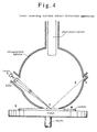
- Fig.4 shows a schematic view of the laser scanning surface defect detection apparatus.
- the apparatus has an integral sphere, a laser, a lens and a photomultiplier.
- the inner wall of the integral sphere is a mirror.
- the integral sphere has an opening at the bottom.
- the semiconductor laser (L) is mounted at a niche on a side of the integral sphere for emitting an inspecting light beam slantingly down.
- the semiconductor laser can be replaced by a gas laser, e.g. a He-Ne laser.
- the integral sphere has an outlet (U) on the other side for taking out a reflected beam.
- the inspection comprises the steps of mounting an object wafer on a stage, bringing the bottom opening of the integral sphere close to the wafer (KTW), irradiating a point (T) on the surface of the wafer by the laser beam (LT), and measuring the power of the reflected light (S).
- the incident beam angle is equal to the reflection angle.
- the laser (L) and the outlet (U) are determined to be symmetric in the integral sphere.
- ⁇ LTK ⁇ UTW. If the surface is flat, all the reflected beams go out through the side opening (U).
- the photomultiplier detects no light. When a defect or a piece of dust lies on the object point (T), a portion of the laser beams is scattered by the defect or dust.
- the scattering beams impinge upon other parts of the wall of the integral sphere.
- the photomultiplier senses the scattered beams.
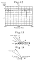
- Fig. 13 shows a bit of dust lying on the surface of the wafer.
- Parallel laser beams are randomly reflected by the dust in the directions E, F, G, etc. Reflected beams do not exit through the outlet (U) but impinge upon the inner wall of the integrated sphere and are reflected to the photomultiplier.
- the photomultiplier measures the scattering light with high sensitivity.
- the photomultiplier detects the existence of a dust at the sampling point (T) by an increase of its photocurrent. The bigger the dust is, the stronger the scattering light becomes.
- the reflected light power is in proportion to the size of the dust.
- Fig.14 shows a notch, a surface defect, on the surface of the silicon wafer.
- the complex refractive index n+jk of silicon has a large real part n and a large imaginary part k for the visible light.
- Laser light is strongly reflected at the interface between air and silicon.
- the notch (M) scatters the beam in other directions (MH) than that of the outlet (U).
- the scattered beams are again reflected by the inner wall of the integral sphere and arrive at the photomultiplier for generating a photocurrent.
- the existence of dust or a defect on the object point of the silicon wafer can easily be detected by the random scattering of light beams.
- the laser scanning surface defect detection apparatus In the silicon semiconductor industry it is well known to use a laser scanning surface defect detection apparatus. It takes only a short time to examine a pretty wide silicon wafer by the laser scanning surface defect detection apparatus. Unlike observation by a microscope, the apparatus can measure the number or the density of defects or dust quantitatively over a wide range. However, the laser scanning surface defect detection apparatus cannot be readily used to examine the surface of diamond.
- M notch
- the beam is reflected by the foreign material substrate along the light path LNQ in Fig.3(a). Since diamond is transparent, the reflection occurs not on the diamond surface but on the interface between the diamond film and the substrate. For this reason, the laser scanning surface defect detection apparatus cannot be applied to the examination of the surface of diamond.
- the Inventors thought that the laser scanning surface defect detection apparatus is a promising candidate for an inspection apparatus for diamond despite the difficulty of transparency.
- One purpose of the present invention is to provide a method of selecting diamond substrates suitable to form a piezoelectric film thereupon.
- This invention coats a diamond film or substrate with a thin metal or non-metal film having a high reflection rate for the laser light.
- the thin film enables the laser scanning surface defect detection apparatus to detect defects or dust on a surface of the diamond, since the thin film reflects the laser light.
- the thin film should be made from a metal or non-metal having a reflectance greater than 50%.
- the thickness of the coating film is less than 100nm.
- the surface of the coating has the same convexities and concavities as the surface of the diamond, since the coating film is thin enough.
- the coating layer transcribes the diamond surface. If the diamond has a surface defect (M), the coating layer has a similar surface defect (K), as shown in Fig.3(b).
- the material of the coating layer is, e.g., aluminum (Al), gold (Au), silver (Ag), copper (Cu), nickel (Ni) or so. Thin film of the metal has a sufficient reflection rate to the laser light. If the diamond has defects or dust, the coating layer has similar anomalies due to the defects or dust at the same spots. The formal anomalies reflect the laser beams at random. Then the laser beams are scattered indirectly by the defects or dust on the diamond.
- the coating layer enables a conventional laser scanning surface defect detection apparatus to detect defects or dust on an object diamond. Thus, the laser scanning surface defect detection apparatus can now be used for the estimation of diamond surfaces.
- Fig.2 shows a diamond crystal covered by a metal coating layer.
- the coated diamond is examined with regard to defects or dust by the laser scanning surface defect detection apparatus. If dust lies on the surface, the dust itself scatters the laser light. The scattered light arrives at the photomultiplier. The existence of the dust can be surely detected by the apparatus.
- defect detection is a problem.
- the metal coating layer has the same geometric anomaly as the defect, because the metal layer is thin enough.
- Most of the laser light is reflected at K point.
- the scattering beam goes along KR. A part of the rest is reflected at M point.
- the scattered beams KR and MI are again reflected at some portions of the integral sphere and reach the photomultiplier.
- the existence of the defect is also detected by the apparatus. Therefore, the laser scanning surface defect detection apparatus which is inherently directed to examining Si wafers can now be diverted to the examination of defects and dust on diamond surfaces by coating the object diamond with a thin opaque layer.
- Diamond films are now examined by the laser scanning surface defect detection apparatus.
- the Inventors discovered that the critical density is 300 particles/cm 2 of the surface defect for diamond films by the examinations. Diamond films which have more than 300 particles/cm 2 defects shall be rejected for the substrate of SAW devices.
- the diamond films with defect density less than 300 particles/cm 2 shall be adopted as a substrate for SAW devices. The most important factor is the surface defect density for estimating diamond films as the substrate of SAW devices.
- the surface roughness Ra of diamond films has an influence upon the quality of the SAW devices in addition to surface defects.
- the surface should have a surface roughness lower than Ra 20 nm. In particular, less than Ra 10nm is preferable for the substrates of SAW devices.
- the roughness is the second criterion for estimating the quality of diamond films.
- Raising productivity requires a wafer size of more than 5 cm (2 inches) of diameter. Namely, the surface area should be wider than 19cm 2 in the case of a circular wafer.
- a pure diamond film is most suitable.
- a diamond coated with a thin carbon is also allowable, since the diamond is directed for a substrate of SAW devices.
- the carbon overcoat layer should be less than 10nm in thickness.
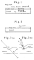
- Fig. 1 shows the following requirements for the diamond film for SAW devices in the present invention.
- a freestanding, homogeneous diamond substrate without foreign material substrate is also available.
- the thickness of the diamond crystal should be 100 ⁇ m to 2000 ⁇ m.
- the complete diamond substrate makes excellent SAW devices.
- Complex substrates having a foreign material, e.g. silicon, substrate and a diamond film coating the substrate are, in general, made use for the substrate of SAW devices.
- the mother foreign material should have a thickness between 0 ⁇ m and 2000 ⁇ m. At the limit of 0 ⁇ m, the case coincides with the former full homogenous diamond substrate.
- the thickness of the diamond film should be more than 1 ⁇ m.
- the mother substrate and the diamond film should have a roughness less than Ra20nm. In particular, the surface roughness of the diamond film preferably is less than Ra10nm.
- Preparatory coating of thin films of a metal or another opaque material enables the laser scanning surface defect detection apparatus to examine the defects of diamond surfaces.
- the examination reveals the density of defects and dust on diamond films or bulks for determining whether piezoelectric films and electrodes should be made upon the diamond samples at a preliminary step.
- Diamond crystals having defect & dust density of more than 300 particles cm -2 cannot form good piezoelectric films and good interdigital transducers thereupon. Higher defect density than 300 particles cm -2 lowers the yield by inviting electrode breaking or other default.
- Diamond surfaces of a defect density lower than 300 particles cm -2 pass the examination. The passed diamond enables manufactures to produce low loss SAW filters available for high frequency by depositing piezoelectric films and making interdigital transducers on the diamond surfaces.
- Diamond can be synthesized by two methods. One way produces a diamond bulk crystal from carbon at a high temperature under ultrahigh pressure. This bulk-production method is called an ultrahigh pressure synthesis. The other way produces a diamond thin film on a mother substrate by supplying hydrogen gas, hydrocarbon gas to the mother substrate, exciting the gas by heat, light or microwave, inducing a chemical reaction of the gas and depositing the reaction product on the mother substrate at a high temperature under reduced pressure. This film-production method is called a vapor phase synthesis. Both methods can produce both diamond single crystals and diamond polycrystals. This invention can be applied both to single crystals and polycrystals of diamond.
- the ultrahigh pressure method can make only a small-sized diamond crystal.
- a big diamond wafer of an area wider than 19cm 2 (2 inches in diameter) can be produced only by the vapor phase synthesis.
- synthesized diamond crystals have some surface roughness which forbids making a uniform piezoelectric film on the diamond. Then, the diamond film should be polished mechanically or chemically.
- This invention makes a diamond crystal shown in Fig.2 by synthesizing a diamond crystal from materials by the methods, polishing the synthesized diamond crystal and coating the polished diamond with a thin metal film of a thickness less than 100nm.
- the diamond crystal is then examined by the laser scanning defect detection apparatus shown in Fig.4.
- the metal thin film reflects the laser beams at point (T) to the outlet (U), if no defect exists at point (T).
- defects broadly include intrinsic, crystallographical defects, hillocks , protrusions, concavities and dust particles on a crystal surface in the description.
- Geometric defects of the diamond are transcribed to the metal surface as shown in Fig.3(b).
- a defect (a dust particle or an intrinsic defect) lies on the interface between the metal and the diamond
- the laser beams are scattered to some spots of the integration sphere and are reflected again to the photomultiplier.
- the photomultiplier senses the defects (dust particles or inherent defects) at point (T) by an increase of the photocurrent. Scanning the integration sphere on the wafer reveals the two-dimensional distribution of the defects including inherent defects and particles. 300 particles/cm 2 is the critical value for defect density. Diamond wafers having a defect density of more than 300 particles/cm 2 should be rejected. Diamond wafers of a defect density less than 300 particles/cm 2 pass the examination.
- a diamond substrate with a thin carbon coating of less than 10nm is permitted for a diamond substrate for producing SAW devices. Preferable roughness of the coating carbon is less than Ra10nm. But less than Ra 20nm is allowable for the surface roughness of the carbon coating.
- the diamond film should be wider than 2 inches in diameter (19cm 2 ) for the standpoint of the economy of wafer processes.
- SAW devices can be fabricated on a diamond wafer less than 19 cm 2 as long as the wafer satisfies the other requirements.
- a homogenous diamond bulk crystal made by the ultrahigh pressure synthesis can be a starting substrate.
- this example adopts a diamond/mother complex substrate made by the vapor phase synthesis method.
- This example shows a substrate consisting of a silicon (Si) mother wafer and a diamond film deposited on the silicon wafer by the microwave plasma CVD method.
- Si single crystal wafer is the most popular mother board.
- Mo 5 can be replaced by a wafer of molybdenum (Mo), nickel (Ni), aluminum nitride (AlN), alumina (Al 2 O 3 ), gallium arsenide (GaAs) or so.
- Mo molybdenum
- Ni nickel
- AlN aluminum nitride
- Al 2 O 3 alumina
- GaAs gallium arsenide
- a wafer having a diameter more than two inches (19cm 2 ) is desirable from the viewpoint of production efficiency.
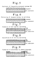
- the synthesized diamond film has a rugged surface having plenty of concavities and convexities. Then, the diamond surface is whetted by a diamond-electrodeposited whetstone which is produced by electrodepositing diamond powder on a turn-table.
- Fig.6 shows a dia/Si complex wafer polished and flattened by the diamond-electrodeposited whetstone. The surface roughness should be less than Ra20nm. Preferably the surface should be further flattened to a smoothness less than Ra10nm.
- the flattened (dia/Si) wafer is now temporarily coated by evaporation with a thin metal, e.g., aluminum film as shown in Fig.2 or Fig.3(b) and examined by the laser scanning surface defect detection apparatus of Fig.4 for searching the defect density.
- the test clarifies the surface roughness ( ⁇ Ra20nm), the defect density ( ⁇ 300 particles cm -2 ) and the carbon coating thickness ( ⁇ 10nm) of the object dia/Si wafers. Wafers failing the test should be rejected.
- Dia/Si wafers which passed the test are employed as substrates of SAW devices.
- the metal thin film is removed from the wafer.
- a piezoelectric film is deposited upon the wafer, for example, by sputtering.
- Fig.7 shows a zinc oxide (ZnO) film for the piezoelectric film.
- Other piezoelectric materials e.g., PZT, LiNbO 3 and LiTaO 3 are also available.
- a metal film, e.g., Al film is further formed on the piezoelectric film by sputtering or evaporation.
- Fig.8 shows the Al/ZnO/dia/Si wafer.
- Photolithography produces interdigital transducers on both sides on a SAW chip by masking the metal film with a resist and etching of the metal by an etchant.
- Fig.9 shows the interdigital transducers formed on the wafer by photolithography.
- Fig.15 denotes an example of an interdigital transducer which consists of two branches having two reciprocally facing parallel stripes in a wavelength ⁇ .
- a SAW device is fabricated by a series of steps of growing a diamond film on a mother material substrate, polishing the diamond film, depositing a piezoelectric film, evaporating a metal film on the piezoelectric film and etching the metal film through a mask.
- the estimation of the diamond should be finished before the formation of the piezoelectric film.
- the electrode breaking rate should be measured by forming interdigital transducers directly on the diamond film without depositing the piezoelectric film and counting the spots of breaking electrode patterns. If the diamond has a poor quality, the interdigital transducers would break at many spots.
- the factor affecting the electrode breaking rate has been sought by forming an interdigital transducer directly upon the diamond, measuring the defect density and considering the correlation between the breaking rate and the diamond film.
- a 35 ⁇ m thick diamond film is grown on the silicon wafer of a 1mm thickness by supplying hydrogen gas containing methane gas of 2 vol% and exciting the mixture gas by the microwave plasma CVD method.
- 100 samples are produced by growing 100 diamond films on 100 Si wafers along the same way.
- the surface roughnesses of the as-grown diamond wafers are, in general, more than Ra1 ⁇ m.
- Substrate silicon wafers thickness 1 mm
- Microwave power 150 W Material gas methane + hydrogen CH 4 :H 2 2:100 flux 50 sccm Gas pressure 5.3 pascals (40 mTorr)
- the microwave CVD made dia/Si complex wafers as shown in Fig.5.
- the 100 samples were polished by a polishing machine having a diamond whetstone.
- the polishing brought about even dia/Si wafers having good smoothness of less than Ra2nm and few defects of less than 50 particles cm -2 defects which were bigger than 0.5 ⁇ m in diameter as shown in Fig.6.
- the average thickness of the diamond films was 20 ⁇ m.
- the X-ray diffraction pattern was examined by the X-ray diffraction apparatus.
- the diffraction pattern revealed an existence of a carbon layer on the diamond film.
- the thickness of the carbon layer was less than 10nm.
- Al films Preliminarily 30nm thick aluminum (Al) films were deposited upon the diamond films of the dia/Si samples by the DC sputtering method.
- the aluminum film coating enables the laser scanning surface defect detection apparatus to examine the surface defects on the diamonds.
- Aluminum film thickness 30 nm DC sputtering power 1.0 kW Reaction gas argon gas 50 sccm Gas pressure 1.0 Pa (7.6mTorr) Substrate temperature room temperature
- the laser scanning surface defect detection apparatus can detect defects or dust on the diamond films.
- This apparatus shoots slantingly the Al-coating diamond film with laser beams, and measures the power of the light scattered from the defects or dust by the photomultiplier(or photomulti-tube).
- a defect is an inherent anomaly but dust is a foreign material lying on the diamond. If the diamond is smooth and flat with little defects, the scattering light power is weak. If the diamond is rugged with many defects, the scattered light power is strong.
- the defect density at the object point is known by the photocurrent. As shown in Fig.4, since the wafer is moved in parallel or in spiral, the existence of defects or dust is examined at all points on the wafer. In the measurement, the bias voltage of the photomultiplier is 550V.
- the relation between the size of defect and the scattered light power is preliminarily determined by the steps of coating a wafer with standard Latex granules of a definite diameter, measuring the power of the light scattered at the granule, replacing the Latex granules with Latex granules of another diameter, measuring the power scattered by the Latex granule again and searching the relation between the granule sizes of Latex and the photocurrent.
- interdigital transducers IDTs
- the Inventors think that defects with a small size less than half of the width have little influence on the electrode formation. But defects with a large size more than half of the width decrease the yield of IDTs.
- the critical size (d) of defects should be determined as a half (W/2) of the width (W) of interdigital transducers.
- the sizes of individual defects cannot be measured. Thus the defect was identified by employing Latex standard granules of a 0.5 ⁇ m diameter.
- a threshold photocurrent was determined as the current induced by a standard granule of a 0.5 ⁇ m diameter.
- a 0.5 ⁇ m diameter defect will cause the same increase of the scattering light power as the 0.5 ⁇ m Latex standard granule.
- the scattered light power is calibrated by Latex standard granules, since the size of the standard granules is uniformly determined.
- the apparatus can sense surface defects which are larger than 0.5 ⁇ m in diameter.
- the depth or height (h) of a defect is another factor affecting the electrode breaking rate.
- the critical depth (or height) is determined to be 10nm for a 1 ⁇ m width electrode. The defects which satisfy d ⁇ W/2 and h ⁇ 10nm should be detected and measured.
- Ten samples were prepared by forming diamond films on ten silicon wafers by a similar method. Ten samples are symbolized by A, B, C, ⁇ ,J. Ten samples were examined with regard to the surface roughness and the defect/dust number. Table 1 shows the surface roughnesses (Ra) and defect numbers of ten samples. The aluminum films were removed, when the defect measurement has once been done. The diamond surfaces appeared.
- Interdigital transducers were made on the diamond layer of the dia/Si wafers.
- the electrode pattern breaking rates were measured.
- the former thin Al films aimed at measurement of defects.
- the present Al coating is directed to making electrodes. Both steps were, by chance, aluminum coating. But the purposes were different.
- the formerly coated aluminum was eliminated.
- a plurality of interdigital transducers were made by evaporating or sputtering aluminum on the (dia/Si) wafers, making a mask pattern by photolithography, and etching the aluminum layer.
- a plurality of pairs of interdigital transducers were produced on each wafer.
- the devices were examined by supplying currents for searching the electrode breaking.
- the breaking rate was calculated by dividing the number of the electrode-breaking devices by the total number of devices.
- the electrode breaking rate is also shown in Table 1.
- the breaking rate is given by an experimental equation which is called "Murphy's plot".
- Murphy's plot is expressed by Cexp(-DA), where C is a constant, D is the defect density and A is the area of IDT patterns. This equation means that if the area for interdigital transducers is wider, the defect density should be smaller for keeping the same yield.
- the distance between neighboring stripes was 1 ⁇ m.
- 400 stripes have a width of about 800 ⁇ m.
- About 3800 sets of 400 electrode stripes were made on each diamond wafer. Then the electrodes were examined by supplying currents. Some electrodes turned out to be broken due to the roughness of the diamond film. The number of breaking electrodes was counted for every diamond wafer sample. The breaking rates were also listed in Table 1. Roughness Ra(nm), Defect density and Breaking rate of aluminum electrodes of samples A to J of (dia/Si)-substrates SAMPLE NO.
- the breaking rates are reversed to Ra for samples E and I.
- Sample H, suffering from a high breaking rate of 91.8%, is useless for the substrate of SAW devices.
- a person who pays attention only to Ra would consider that sample H must be a good substrate.
- Ra is not a reliable factor for foreseeing the quality of electrodes formed upon the sample.
- Sample B enjoys 0% of pattern breaking rate, since it has a small defect density of 287 particles/cm 2 .
- Sample A exhibits 0 % breaking rate due to the very small defect density of 80 particles/cm 2 .
- Sample C has still a low defect density of 462 particles cm -2 which suppresses the breaking rate to 1.2%.
- Sample D has a defect density of 812 particles cm -2 which is about twice as many as sample C.
- the electrode breaking rate is also doubled to 4.8%.
- Sample F which has defects of 2436 particles cm -2 is accompanied by a high breaking rate 33.8%.
- Sample G with a defect density 3788 particles cm -2 is afflicted with a high breaking rate 72.3%.
- sample H has a very high breaking rate 91.8% due to the large defect density of 4689 particles cm -2 .
- the examination by the laser scanning surface defect detection apparatus gives the most suitable estimation for the surface states of diamond wafers.
- An ideal condition is, of course, 0% of breaking rate.
- the defect (and dust) density should be less than 300 particles cm -2 , because sample B of 0 % has a defect density less than 300 particles cm -2 but sample C of 1.2% has a defect density more than 300 particles cm -2 .
- 300 particles cm -2 is the critical value ruling the break of electrode patterns.
- What affects the break of electrode patterns is not the surface roughness but the defect density.
- the Inventors succeeded in examining the defect on diamond crystals by coating the object diamond with a thin metal film and measuring the scattering light in the laser scanning surface defect detection apparatuses which have been widely employed for estimation of silicon wafers.
- the new estimation method using the laser scanning surface defect detection apparatus can give a definite requirement of diamond films or bulks suitable for the substrates of SAW devices.
- the preliminary estimation can prophesy that the object diamond crystals are appropriate for the substrates for making piezoelectric films and producing interdigital transducers.
- SAW devices should be made only on the diamond substrates which passed the examination.
- the samples which fail in the examination should be rejected without making piezoelectric films and interdigital transducers (IDT).
- the estimation can save much time, energy and resources.
- Piezoelectric ZnO films of a 1050 nm thickness were formed upon the dia/Si substrates of sample A and sample B by an RF sputtering method.
- Substrates dia/Si wafers sample A, sample B Target ZnO sintered plate RF power 500 W (13.56MHz)
- Reaction gas Ar+O 2 Ar:O 2 1:1 gas flow 50 sccm
- Substrate temperature 150°C Speed of deposition 5 nm/min Thickness 1050 nm (1.05 ⁇ m)
- Complex wafers of ZnO/dia/Si were made from samples A and B by the above way.
- Interdigital transducers having the following parameters were formed by eliminating parts of the aluminum layer selectively by photolithography.
- Line Width of IDTs 0.8 ⁇ m (central frequency 1.75 GHz)
- Fig. 15 shows the IDT pattern.
- Transmission loss and the conversion loss of the SAW devices were measured by a spectrum network analyzer (HP8753c).
- AC power of 1GHz to 2GHz was applied to one side electrode (electrode 1).
- the electric power of the input electrode 1 and the electric power of the output (counterpart) electrode 2, that is, scattering parameters were measured.
- S11 is a reflection power ratio which is a quotient of the reflected power to the electrode 1 to the input power of the electrode 1, when the AC power is supplied to the electrode 1.
- S22 is a reflection power ratio which is a quotient of the reflected power to the electrode 2 to the input power to the electrode 2, when AC power is supplied to the electrode 2.
- S12 is a transmission power ratio which is a quotient of the power arrived at the electrode 2 to the input power to the electrode 1, when AC power is supplied to the electrode 1.
- S21 is a transmission power ratio which is a quotient of the power arrived at the electrode 1 to the input power to the electrode 2, when AC power is supplied to the electrode 2.
- Fig.10 shows the transmission power ratio (S12) as a function of the frequency of signals.
- the abscissa is the frequency (MHz).
- the ordinate is the transmission power ratio (dB).
- 1.78 GHz (1780 MHz) gives a peak of the transmission power of -8.2dB.
- the maximum transmission power ratio is -0.82dB.
- the loss 8.2dB includes all the resistance loss at electrodes, the bilateral loss and the conversion loss. The real transmission loss can be calculated by subtracting these losses from the total loss 8.2dB.
- the resistance loss is calculated to be 1.0 dB for an electrode stripe of a 80nm thickness and a 0.8 ⁇ m width.
- the bilateral loss is 6db, because the power is halved at the input electrode.
- Fig.11 shows S11 and Fig.12 shows S22.
- the loss is about 0.3dB both for S11 and for S22.
- the conversion loss occurs at both the input and the output electrodes.
- the conversion loss is 0.6dB at both electrodes.
- the sum of the resistance loss, the bilateral loss and the conversion loss is 7.6dB.
- the total loss for 1.78GHz is 8.2dB from S12.
- the propagation loss is only 0.6dB which is a difference between the total loss 8.2dB and the sum 7.6dB of the three losses. 0.6dB is a small propagation loss.
- SAW devices have been fabricated on samples C to I in a similar manner.
- the electrodes of the SAW devices are examined by electric property measurement, optical microscope observation and electron microscope observation. Some SAW devices are suffering from electrode breaking. Others are immune from electrode breaking. The properties of SAW devices without electrode breaking are tested.
- All the samples of C to I have insertion loss higher than 13dB. This examination reveals bad crystallographic properties of the piezoelectric films of samples C to I. The surface defects of diamond films worsen the crystallographic properties of the piezoelectric films. The bad crystallography of piezoelectric films raises the propagation loss of the SAW devices made on samples C to I.
- This invention examines surface defects of diamond films or bulks by covering the object diamond surfaces with thin metal films and measuring defects by the laser scanning surface defect detection apparatus.
- the preliminary examination can foresee the properties of SAW devices which will be made on the diamond crystals.
- SAW devices should be fabricated only upon the samples having diamond surface of small defect density, for example, less than 300 particles cm -2 .
- the definition of a defect includes the critical size which depends upon the period of the electrodes.
- the defect density of the same diamond is different for different periods of the electrodes of SAW devices.
- Low defect density diamond films or bulks bring about zero or small enough electrode breaking rates when electrodes are made thereon.
- Low propagation loss SAW devices can be produced by depositing piezoelectric films on the low defect density diamonds and making interdigital transducers on the piezoelectric films.
Landscapes
- Physics & Mathematics (AREA)
- Acoustics & Sound (AREA)
- Engineering & Computer Science (AREA)
- Manufacturing & Machinery (AREA)
- Surface Acoustic Wave Elements And Circuit Networks Thereof (AREA)
- Crystals, And After-Treatments Of Crystals (AREA)
- Investigating Or Analyzing Materials By The Use Of Ultrasonic Waves (AREA)
- Testing Or Measuring Of Semiconductors Or The Like (AREA)
Claims (3)
- Verfahren zum Schätzen der Dichte von Oberflächenfehlern oder Teilchen auf einem Diamant-Wafer, wobei das Verfahren die folgenden Schritte umfasst:Beschichten einer Oberfläche des Diamant-Wafers mit einem dünnen opaken Film mit einer Dicke von weniger als 100 nm,Belichten der beschichteten Oberfläche des Diamant-Wafers mit Laserstrahlen von einer Laserabtast-Oberflächenfehler-Erfassungsvorrichtung, wobei die Laserstrahlen an einer Oberfläche des Beschichtungsfilms sowie an einer Grenzfläche zwischen dem Beschichtungsfilm und der Oberfläche des Diamant-Wafers reflektiert werden, undZählen der durch Oberflächenfehler oder Teilchen auf der Oberfläche des Diamant-Wafers gestreuten Strahlen.
- Verfahren nach Anspruch 1, wobei der opake Film zum Beschichten des Diamant-Wafers ein Metallfilm oder ein Nichtmetallfilm mit einem Reflexionsvermögen von mehr als 50 % ist.
- Verfahren nach Anspruch 2, wobei der opake Film zum Beschichten des Diamant-Wafers ein Aluminiumfilm ist, der durch Sputtern abgeschieden wird.
Applications Claiming Priority (3)
| Application Number | Priority Date | Filing Date | Title |
|---|---|---|---|
| JP29026297 | 1997-10-06 | ||
| JP290262/97 | 1997-10-06 | ||
| JP29026297A JP3168961B2 (ja) | 1997-10-06 | 1997-10-06 | ダイヤモンド基板及びダイヤモンド基板の評価方法並びにダイヤモンド表面弾性波フィルタ |
Publications (3)
| Publication Number | Publication Date |
|---|---|
| EP0909025A2 EP0909025A2 (de) | 1999-04-14 |
| EP0909025A3 EP0909025A3 (de) | 2000-10-18 |
| EP0909025B1 true EP0909025B1 (de) | 2005-02-09 |
Family
ID=17753868
Family Applications (1)
| Application Number | Title | Priority Date | Filing Date |
|---|---|---|---|
| EP98308109A Expired - Lifetime EP0909025B1 (de) | 1997-10-06 | 1998-10-06 | Bestimmungsverfahren eines Diamantwafer |
Country Status (8)
| Country | Link |
|---|---|
| US (3) | US6210780B1 (de) |
| EP (1) | EP0909025B1 (de) |
| JP (1) | JP3168961B2 (de) |
| KR (1) | KR100511806B1 (de) |
| CA (2) | CA2249276C (de) |
| DE (1) | DE69828933T2 (de) |
| MY (1) | MY117806A (de) |
| SG (1) | SG75884A1 (de) |
Families Citing this family (32)
| Publication number | Priority date | Publication date | Assignee | Title |
|---|---|---|---|---|
| JP3168961B2 (ja) * | 1997-10-06 | 2001-05-21 | 住友電気工業株式会社 | ダイヤモンド基板及びダイヤモンド基板の評価方法並びにダイヤモンド表面弾性波フィルタ |
| US6580196B1 (en) * | 1999-08-17 | 2003-06-17 | Shin-Etsu Chemical Co., Ltd. | Piezoelectric single crystal wafer |
| US7132309B2 (en) * | 2003-04-22 | 2006-11-07 | Chien-Min Sung | Semiconductor-on-diamond devices and methods of forming |
| US6814130B2 (en) * | 2000-10-13 | 2004-11-09 | Chien-Min Sung | Methods of making diamond tools using reverse casting of chemical vapor deposition |
| US7011134B2 (en) * | 2000-10-13 | 2006-03-14 | Chien-Min Sung | Casting method for producing surface acoustic wave devices |
| US7057256B2 (en) | 2001-05-25 | 2006-06-06 | President & Fellows Of Harvard College | Silicon-based visible and near-infrared optoelectric devices |
| US7442629B2 (en) | 2004-09-24 | 2008-10-28 | President & Fellows Of Harvard College | Femtosecond laser-induced formation of submicrometer spikes on a semiconductor substrate |
| TWI264869B (en) * | 2001-10-05 | 2006-10-21 | Sumitomo Electric Industries | Diamond substrate for surface acoustic wave device, and surface acoustic wave device |
| US6906451B2 (en) | 2002-01-08 | 2005-06-14 | Murata Manufacturing Co., Ltd. | Piezoelectric resonator, piezoelectric filter, duplexer, communication apparatus, and method for manufacturing piezoelectric resonator |
| GB2433737B (en) * | 2002-11-21 | 2007-08-15 | Element Six Ltd | Optical quality diamond material |
| GB0227261D0 (en) | 2002-11-21 | 2002-12-31 | Element Six Ltd | Optical quality diamond material |
| US7481879B2 (en) * | 2004-01-16 | 2009-01-27 | Sumitomo Electric Industries, Ltd. | Diamond single crystal substrate manufacturing method and diamond single crystal substrate |
| US7846767B1 (en) | 2007-09-06 | 2010-12-07 | Chien-Min Sung | Semiconductor-on-diamond devices and associated methods |
| US8183086B2 (en) * | 2009-06-16 | 2012-05-22 | Chien-Min Sung | Diamond GaN devices and associated methods |
| US9673243B2 (en) | 2009-09-17 | 2017-06-06 | Sionyx, Llc | Photosensitive imaging devices and associated methods |
| US9911781B2 (en) | 2009-09-17 | 2018-03-06 | Sionyx, Llc | Photosensitive imaging devices and associated methods |
| WO2011123553A2 (en) * | 2010-04-02 | 2011-10-06 | Visa International Service Association | Crack embossing using diamond technology |
| US8692198B2 (en) | 2010-04-21 | 2014-04-08 | Sionyx, Inc. | Photosensitive imaging devices and associated methods |
| EP2583312A2 (de) | 2010-06-18 | 2013-04-24 | Sionyx, Inc. | Lichtempfindliche hochgeschwindigkeitsvorrichtungen und verfahren dafür |
| US9496308B2 (en) | 2011-06-09 | 2016-11-15 | Sionyx, Llc | Process module for increasing the response of backside illuminated photosensitive imagers and associated methods |
| EP2732402A2 (de) | 2011-07-13 | 2014-05-21 | Sionyx, Inc. | Biometrische bildgebungsvorrichtungen und entsprechende verfahren |
| WO2013120093A1 (en) * | 2012-02-10 | 2013-08-15 | Sionyx, Inc. | Low damage laser-textured devices and associated methods |
| US9064764B2 (en) | 2012-03-22 | 2015-06-23 | Sionyx, Inc. | Pixel isolation elements, devices, and associated methods |
| WO2014027538A1 (ja) * | 2012-08-17 | 2014-02-20 | 日本碍子株式会社 | 複合基板,弾性表面波デバイス及び複合基板の製造方法 |
| US9259818B2 (en) * | 2012-11-06 | 2016-02-16 | Sinmat, Inc. | Smooth diamond surfaces and CMP method for forming |
| JP6466346B2 (ja) | 2013-02-15 | 2019-02-06 | サイオニクス、エルエルシー | アンチブルーミング特性を有するハイダイナミックレンジcmos画像センサおよび関連づけられた方法 |
| US9939251B2 (en) | 2013-03-15 | 2018-04-10 | Sionyx, Llc | Three dimensional imaging utilizing stacked imager devices and associated methods |
| US9209345B2 (en) | 2013-06-29 | 2015-12-08 | Sionyx, Inc. | Shallow trench textured regions and associated methods |
| DE102017112659B4 (de) * | 2017-06-08 | 2020-06-10 | RF360 Europe GmbH | Elektrischer Bauelementwafer und elektrisches Bauelement |
| JP2019029941A (ja) * | 2017-08-02 | 2019-02-21 | 株式会社ディスコ | 弾性波デバイス用基板の製造方法 |
| JP7712518B2 (ja) * | 2020-05-22 | 2025-07-24 | フラウンホーファー ユーエスエイ インコーポレイテッド | 機械学習を用いたダイヤモンドの合成システムおよび方法 |
| TWI876530B (zh) * | 2023-09-13 | 2025-03-11 | 晶呈科技股份有限公司 | 晶圓表面膜層的檢測方法 |
Family Cites Families (18)
| Publication number | Priority date | Publication date | Assignee | Title |
|---|---|---|---|---|
| CH535430A (de) | 1971-02-17 | 1973-03-31 | Gretag Ag | Verfahren und Vorrichtung zur Detektierung von staubförmigen Partikeln |
| DE3325251A1 (de) * | 1983-07-13 | 1985-01-24 | Brown, Boveri & Cie Ag, 6800 Mannheim | Verfahren zum pruefen und nachbessern von auf bauelementen aufgetragenen schutzschichten |
| US4664514A (en) | 1984-11-06 | 1987-05-12 | General Electric Company | Method of enhancing surface features and detecting same |
| US4978862A (en) * | 1988-07-13 | 1990-12-18 | Vti, Inc. | Method and apparatus for nondestructively measuring micro defects in materials |
| US5772760A (en) * | 1991-11-25 | 1998-06-30 | The University Of Chicago | Method for the preparation of nanocrystalline diamond thin films |
| JPH06326548A (ja) * | 1993-05-14 | 1994-11-25 | Kobe Steel Ltd | 高配向性ダイヤモンド薄膜を使用した表面弾性波素子 |
| US5674572A (en) * | 1993-05-21 | 1997-10-07 | Trustees Of Boston University | Enhanced adherence of diamond coatings employing pretreatment process |
| JP3774904B2 (ja) * | 1994-01-27 | 2006-05-17 | 住友電気工業株式会社 | 平坦なダイヤモンド膜の合成法とダイヤモンド自立膜及びダイヤモンド膜の研磨方法 |
| JP3344441B2 (ja) * | 1994-03-25 | 2002-11-11 | 住友電気工業株式会社 | 表面弾性波素子 |
| DE69503285T2 (de) * | 1994-04-07 | 1998-11-05 | Sumitomo Electric Industries | Diamantwafer und Verfahren zur Herstellung eines Diamantwafers |
| DE69526129T2 (de) * | 1994-05-23 | 2002-08-22 | Sumitomo Electric Industries, Ltd. | Verfahren und Vorrichtung zum Herstellen eines mit hartem Material bedeckten Halbleiters durch Polieren |
| DE69508679T2 (de) * | 1994-06-09 | 1999-08-12 | Sumitomo Electric Industries, Ltd., Osaka | Wafer und Verfahren zur Herstellung eines Wafers |
| JP3282645B2 (ja) * | 1994-06-16 | 2002-05-20 | 住友電気工業株式会社 | 表面弾性波素子 |
| JP3295921B2 (ja) * | 1994-06-20 | 2002-06-24 | 住友電気工業株式会社 | 表面弾性波素子用ダイヤモンド基材及び素子 |
| DE69535861D1 (de) * | 1994-06-24 | 2008-11-27 | Sumitomo Electric Industries | Wafer und sein Herstellungsverfahren |
| US5576589A (en) * | 1994-10-13 | 1996-11-19 | Kobe Steel Usa, Inc. | Diamond surface acoustic wave devices |
| GB9513426D0 (en) * | 1995-06-29 | 1997-03-12 | Diamanx Products Ltd | Diamond treatment |
| JP3168961B2 (ja) * | 1997-10-06 | 2001-05-21 | 住友電気工業株式会社 | ダイヤモンド基板及びダイヤモンド基板の評価方法並びにダイヤモンド表面弾性波フィルタ |
-
1997
- 1997-10-06 JP JP29026297A patent/JP3168961B2/ja not_active Expired - Lifetime
-
1998
- 1998-09-25 SG SG1998004172A patent/SG75884A1/en unknown
- 1998-10-02 KR KR1019980041638A patent/KR100511806B1/ko not_active Expired - Fee Related
- 1998-10-05 MY MYPI98004547A patent/MY117806A/en unknown
- 1998-10-05 CA CA 2249276 patent/CA2249276C/en not_active Expired - Fee Related
- 1998-10-05 CA CA 2508253 patent/CA2508253C/en not_active Expired - Fee Related
- 1998-10-06 EP EP98308109A patent/EP0909025B1/de not_active Expired - Lifetime
- 1998-10-06 US US09/166,840 patent/US6210780B1/en not_active Expired - Lifetime
- 1998-10-06 DE DE1998628933 patent/DE69828933T2/de not_active Expired - Lifetime
-
2000
- 2000-04-05 US US09/543,415 patent/US6356006B1/en not_active Expired - Fee Related
-
2001
- 2001-04-05 US US09/825,887 patent/US6320296B1/en not_active Expired - Fee Related
Also Published As
| Publication number | Publication date |
|---|---|
| CA2249276A1 (en) | 1999-04-06 |
| CA2508253A1 (en) | 1999-04-06 |
| JPH11116387A (ja) | 1999-04-27 |
| CA2508253C (en) | 2008-07-08 |
| US6356006B1 (en) | 2002-03-12 |
| US6210780B1 (en) | 2001-04-03 |
| MY117806A (en) | 2004-08-30 |
| US6320296B1 (en) | 2001-11-20 |
| EP0909025A2 (de) | 1999-04-14 |
| SG75884A1 (en) | 2000-10-24 |
| KR19990036843A (ko) | 1999-05-25 |
| CA2249276C (en) | 2007-06-26 |
| EP0909025A3 (de) | 2000-10-18 |
| US20010044029A1 (en) | 2001-11-22 |
| JP3168961B2 (ja) | 2001-05-21 |
| DE69828933D1 (de) | 2005-03-17 |
| DE69828933T2 (de) | 2006-05-11 |
| KR100511806B1 (ko) | 2006-01-12 |
Similar Documents
| Publication | Publication Date | Title |
|---|---|---|
| EP0909025B1 (de) | Bestimmungsverfahren eines Diamantwafer | |
| Yamamoto et al. | Characterization of ZnO piezoelectric films prepared by rf planar‐magnetron sputtering | |
| US7579759B2 (en) | Surface acoustic wave (SAW) devices based on cubic boron nitride/diamond composite structures | |
| EP0676485B1 (de) | Diamantwafer und Verfahren zur Herstellung eines Diamantwafers | |
| EP0674385B1 (de) | Orientierbares Material, orientierbares Substrat und Oberflächenwellenanordnung | |
| EP0726649B1 (de) | Akustische Oberflächenwellenanordnung | |
| Assouar et al. | Synthesis and microstructural characterisation of reactive RF magnetron sputtering AlN films for surface acoustic wave filters | |
| Capilla et al. | High-acoustic-impedance tantalum oxide layers for insulating acoustic reflectors | |
| EP0688098B1 (de) | Akustische Oberflächenwellenanordnung von Diamant-LiTaO3 | |
| US6858969B2 (en) | Surface acoustic wave devices based on unpolished nanocrystalline diamond | |
| EP0766383B1 (de) | Akustische Oberflächenwellenanordnung mit Diamant-ZnO mit verhältnismässig dünner piezoelektrischer ZnO-Schicht | |
| Elmazria et al. | Effect of diamond nucleation process on propagation losses of AlN/diamond SAW filter | |
| Mortet et al. | Deposition of Aluminium Nitride Film by Magnetron Sputtering for Diamond‐Based Surface Acoustic Wave Applications | |
| Ishihara et al. | Synthesis and surface acoustic wave property of aluminum nitride thin films fabricated on silicon and diamond substrates using the sputtering method | |
| US20080118661A1 (en) | Thin Film Producing Method | |
| Liaw et al. | The SAW characteristics of sputtered aluminum nitride on silicon | |
| Mortet et al. | Structural characterisations of AlN/diamond structures used for surface acoustic wave device applications | |
| Kim et al. | Velocity surface measurements for ZnO films over {001}‐cut GaAs | |
| Hong et al. | E ect of thermal annealing on the SAW properties of AlN films deposited on Si substrate | |
| JPH08330882A (ja) | 表面弾性波素子基板及びその製造方法 | |
| KR102402296B1 (ko) | 압전성 재료 기판과 지지 기판의 접합체 | |
| Dogheche et al. | Growth process and surface acoustic wave characteristics of LiNbO3/diamond/silicon multilayered structures | |
| Sinno | ZnO thin-film optimization towards the fabrication of high-frequency ultrasound transducers | |
| Elmazria et al. | Effect of the nucleation process on freestanding AlN/diamond SAW filter characteristics | |
| Paradis et al. | Fabrication of Sputtered Aluminum Nitride on Sapphire for Application in UHF SAW Frequency Filters. |
Legal Events
| Date | Code | Title | Description |
|---|---|---|---|
| PUAI | Public reference made under article 153(3) epc to a published international application that has entered the european phase |
Free format text: ORIGINAL CODE: 0009012 |
|
| AK | Designated contracting states |
Kind code of ref document: A2 Designated state(s): DE FR GB NL |
|
| AX | Request for extension of the european patent |
Free format text: AL;LT;LV;MK;RO;SI |
|
| PUAL | Search report despatched |
Free format text: ORIGINAL CODE: 0009013 |
|
| AK | Designated contracting states |
Kind code of ref document: A3 Designated state(s): AT BE CH CY DE DK ES FI FR GB GR IE IT LI LU MC NL PT SE |
|
| AX | Request for extension of the european patent |
Free format text: AL;LT;LV;MK;RO;SI |
|
| 17P | Request for examination filed |
Effective date: 20001010 |
|
| AKX | Designation fees paid |
Free format text: DE FR GB NL |
|
| 17Q | First examination report despatched |
Effective date: 20040329 |
|
| GRAP | Despatch of communication of intention to grant a patent |
Free format text: ORIGINAL CODE: EPIDOSNIGR1 |
|
| RTI1 | Title (correction) |
Free format text: METHOD OF ESTIMATING A DIAMOND WAFER |
|
| GRAS | Grant fee paid |
Free format text: ORIGINAL CODE: EPIDOSNIGR3 |
|
| GRAA | (expected) grant |
Free format text: ORIGINAL CODE: 0009210 |
|
| AK | Designated contracting states |
Kind code of ref document: B1 Designated state(s): DE FR GB NL |
|
| REG | Reference to a national code |
Ref country code: GB Ref legal event code: FG4D |
|
| REF | Corresponds to: |
Ref document number: 69828933 Country of ref document: DE Date of ref document: 20050317 Kind code of ref document: P |
|
| PLBE | No opposition filed within time limit |
Free format text: ORIGINAL CODE: 0009261 |
|
| STAA | Information on the status of an ep patent application or granted ep patent |
Free format text: STATUS: NO OPPOSITION FILED WITHIN TIME LIMIT |
|
| ET | Fr: translation filed | ||
| 26N | No opposition filed |
Effective date: 20051110 |
|
| PGFP | Annual fee paid to national office [announced via postgrant information from national office to epo] |
Ref country code: NL Payment date: 20111020 Year of fee payment: 14 Ref country code: FR Payment date: 20111103 Year of fee payment: 14 |
|
| REG | Reference to a national code |
Ref country code: NL Ref legal event code: V1 Effective date: 20130501 |
|
| REG | Reference to a national code |
Ref country code: FR Ref legal event code: ST Effective date: 20130628 |
|
| PG25 | Lapsed in a contracting state [announced via postgrant information from national office to epo] |
Ref country code: NL Free format text: LAPSE BECAUSE OF NON-PAYMENT OF DUE FEES Effective date: 20130501 Ref country code: FR Free format text: LAPSE BECAUSE OF NON-PAYMENT OF DUE FEES Effective date: 20121031 |
|
| PGFP | Annual fee paid to national office [announced via postgrant information from national office to epo] |
Ref country code: DE Payment date: 20171115 Year of fee payment: 20 |
|
| PGFP | Annual fee paid to national office [announced via postgrant information from national office to epo] |
Ref country code: GB Payment date: 20171106 Year of fee payment: 20 |
|
| REG | Reference to a national code |
Ref country code: DE Ref legal event code: R071 Ref document number: 69828933 Country of ref document: DE |
|
| REG | Reference to a national code |
Ref country code: GB Ref legal event code: PE20 Expiry date: 20181005 |
|
| PG25 | Lapsed in a contracting state [announced via postgrant information from national office to epo] |
Ref country code: GB Free format text: LAPSE BECAUSE OF EXPIRATION OF PROTECTION Effective date: 20181005 |