EP0908050B1 - Data transmission - Google Patents
Data transmission Download PDFInfo
- Publication number
- EP0908050B1 EP0908050B1 EP97927275A EP97927275A EP0908050B1 EP 0908050 B1 EP0908050 B1 EP 0908050B1 EP 97927275 A EP97927275 A EP 97927275A EP 97927275 A EP97927275 A EP 97927275A EP 0908050 B1 EP0908050 B1 EP 0908050B1
- Authority
- EP
- European Patent Office
- Prior art keywords
- data
- threshold
- training sequence
- signal
- levels
- Prior art date
- Legal status (The legal status is an assumption and is not a legal conclusion. Google has not performed a legal analysis and makes no representation as to the accuracy of the status listed.)
- Expired - Lifetime
Links
Images
Classifications
-
- H—ELECTRICITY
- H04—ELECTRIC COMMUNICATION TECHNIQUE
- H04N—PICTORIAL COMMUNICATION, e.g. TELEVISION
- H04N7/00—Television systems
- H04N7/025—Systems for the transmission of digital non-picture data, e.g. of text during the active part of a television frame
Definitions
- This invention relates to data transmission and in particular to data transmission in which a multi-level representation of a digital signal is transmitted.
- Digital data represents a signal that has been quantised in both time and amplitude.
- the digital data thus approximates the actual value of an analogue signal. If an analogue signal is digitised, the range of the analogue signal is divided into a number of levels e.g. 16, the analogue signal is sampled at set intervals and the appropriate level at that instant is determined. Since only 16 levels are used, the level which is closest to the actual level is chosen. A signal that is reconstructed from this digital data resembles but is not exactly the same as the original analogue signal.
- a signal is represented by 0 or 1, a 0 being a 0 V pulse and a 1 being a 5 V pulse for example. If a sample of an input signal has an amplitude greater than half of the maximum range, the signal sample is represented by a 1. A 0 will result from samples having an amplitude less than half. Thus a series of ones and zeros is produced.
- a receiver needs to know the threshold between the two levels. This is usually done by the transmitter signalling to the receiver the maximum range of the signal, the number of levels and the spacing of the levels e.g. if they are linearly spaced etc. The receiver then determines the threshold(s) and decodes an incoming signal. In practice, in a multi-level system there are distortions in the signal due to the response of the network, namely overshoot and ringing. The instantaneous level of any received sample is not only dependent on the transmitted sample, but on the recent previously transmitted samples and possibly the subsequently transmitted sample or samples.
- U.S. patent 5,287,540 describes a digital detector with a comparator for comparing four-level input signals with decision levels to recover the transmitted symbols, and has updating logic for updating the decision levels, based on a "preamble" at the beginning of each received signal.
- a data transmission system comprising: a transmitter having means to encode an input signal to form coded data, each element of said coded data having one of at least two discrete signal magnitude levels, the encoding means including means to generate a predetermined training sequence of data having elements assuming said discrete levels; and a receiver having decoding means to receive said coded data and to compare it with a threshold or thresholds to allow the discrete levels to be distinguishable from each other, said receiver further having threshold adaptation means operable on the basis of the received training sequence to adapt said thresholds, wherein the threshold adaptation means includes means to monitor the effect of at least one of the elements of the training sequence on another of said elements of the training sequence and adapt the threshold(s) accordingly.
- Such a system allows the receiver continually to adapt the threshold(s) in dependence on the dynamic conditions of the transmission link between the transmitter and receiver, and the effects of the transmission link on groups of elements is accounted for.
- the invention also relates to the transmitter and a receiver as defined in claims 7 and 11.
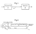
- the digital data transmission system comprises a transmitter 20, a receiver 30 and a communications link 40.
- Data is transmitted from the transmitter 20 to the receiver 30 via the communications link 40 which may take any suitable form.
- the communications link 40 may be part of a Public Switched Telephone Network (PSTN), a dedicated line such as provided by an Integrated Services Digital Network (ISDN), a radio link, coaxial cable, optical fibre etc.
- PSTN Public Switched Telephone Network
- ISDN Integrated Services Digital Network
- radio link coaxial cable, optical fibre etc.
- the data transmission system to be described refers to the transmission of data representing a video image.
- the invention is applicable to any system that transmits multi-level digital data, in particular for transmission over an analogue transmission link e.g. cable modems, higher bit rate teletext services.
- the data transmission system to be described is suitable for distributing digital television signals to customers over an analogue hybrid fibre-coax network.
- the digital signals In order to use existing analogue network infrastructure, the digital signals must be capable of being transmitted over the existing network in the same way as an ordinary TV channel.
- the digital signal must therefore occupy a similar bandwidth to the ordinary TV channel (6-7 MHz). It must also 'look' like a TV signal in terms of amplitude and have regular 'line' sync pulses at 15.625 kHz, as some dc restoration in the network relies on this. Signal to noise ratio is around 50dB and there are non-linearities such as differential gain errors and sync pulse clipping to overcome.
- the invention uses multi-level coding, whereby serial digital data is split into symbols of n bits. Each symbol is then coded as one of 2 n discrete levels within the active video region.
- ADCs video analogue-to-digital converters
- FIG. 2 A diagram of the waveform to be transmitted is shown in Figure 2. It consists of a synchronisation (sync.) pulse 2 having a standard width and amplitude, repeating at 15.625 kHz. This is preceded and succeeded respectively by a front porch 4 and a back porch 6 to allow readily available TV sync pulse separators and analogue to digital converters to be used.
- a synchronisation (sync.) pulse 2 having a standard width and amplitude, repeating at 15.625 kHz. This is preceded and succeeded respectively by a front porch 4 and a back porch 6 to allow readily available TV sync pulse separators and analogue to digital converters to be used.
- a start pulse which is used by the receiver to determine the best sampling position.
- S start pulse
- T training sequence
- M marker to allow the start of the training sequence to be determined. The exact nature and function of the training sequence will be described later.
- valid data symbols D Each is nominally 148ns wide and is represented by one of eight distinct levels, nominally 0.1 V apart.
- the valid data can be split up into blocks to allow the addition of a block based forward error corrector (FEC).
- FEC forward error corrector
- One overhead in systems which use block based FEC is the need to add framing bits to define the block boundaries, and the hardware at the receiver to search for and lock onto the framing. This is not necessary in this scheme as the data is already divided into 'lines' which can be further subdivided into blocks.
- error corrector block size and total number of symbols per line depends on the required bit rate and the correcting power of the FEC.
- the proposed system uses a BCH (Bose-Chaudhuri Hocquenghem) forward error corrector and divides the line into 17 blocks of 63 bits.
- the FEC is capable of correcting one bit in error in each block.
- the symbols are Gray coded so that adjacent levels represent bit patterns with only one bit difference.
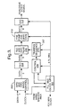
- the transmitter 20 can either be a slave to the MPEG multiplexer clock, or a master clock provider.
- the phase locked loop (PLL) and clock generator 201 generates the 6.75MHz symbol clock locked to the 15MHz data bit clock.
- the incoming binary digital data is split into 3-bit symbols by a serial-in-parallel-out (SIPO) shift register 202 and stored in a first in, first out (FIFO) buffer 204.
- the FIFO 204 buffers the symbols between the continuous input data rate and the 'bursty' line and block structure.
- the symbols are read from the FIFO 204 and BCH FEC check bits are added by FEC encoder 206.
- the sync pulse, black level (i.e. front porch and back porch), start pulse (S) and training sequence are added by a unit 207 under control of a control block 208.
- the data is then Gray coded and converted to an 8-bit representation 210 before being presented to the digital-to-analogue converter DAC 212.
- a certain amount of pre-compensation can be added at this stage to help reduce overshoot in the network. This effectively reduces the rise-time of the edges within the signal.
- the analogue output of the DAC 212 can then be transmitted across the network in the same way as a normal TV channel.
- An analogue post filter can be added if necessary to band limit the signal to suit the network.
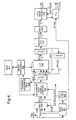
- a block diagram of the receiver 30 is shown in Figure 4.
- a sync. separator 301 extracts sync. and black level pulses from the incoming signal.
- a PLL and voltage-controlled crystal oscillator (VCXO) 302 generates a line locked 27 MHz clock.
- An 8-bit ADC 303 digitises the incoming signal into an 8 bit signal.
- the ADC 303 has an on-chip clamp and automatic gain control (AGC) which uses the sync. and black level pulses.
- AGC automatic gain control
- the effect of the AGC is to set the digital output at the base of the sync. pulse 2 to 0 and the black level (i.e. the level of the front and back porch 4 and 6) to 63.
- a nominal maximum level video input of say 0.7V is then given a level of 213.
- the ADC is clocked at 27 MHz.
- Logic 304 which follows the ADC 303 contains a state machine which searches for the start pulses (S) after each line sync pulse 2.
- S start pulses
- the start pulse S will be rounded after having passed through the network and the best sampling position is taken as the sample closest to its peak. An inverted version of the clock can be used if this gives a better sample position.
- the training sequence is 1024 lines long and occupies five symbols at the start of each line between the start pulse S and the valid data symbols D.
- the first symbol (M) in the sequence indicates the start of the training sequence; it is high (level 7) on the first line of the sequence and low (level 0) on all the other lines.
- the next three symbols T 1 , T 2 , T 3 symbols count through a sequence of all the possible combinations of eight levels for the three symbols (8 3 combinations), line by line, with the last symbol T 4 low (level 0) or high (level 7) giving 2x8 3 i.e. 1024 combinations, occupying 1024 lines (approx. 65 mSec.)
- the level of the fourth symbol T 3 in the training sequence of each line is sampled and stored in a FIFO 306.
- the FIFO 306 contains examples of all levels of the fourth symbol with all combinations of the two preceding symbols T 1 , T 2 and the succeeding symbol T 4 being low or high.
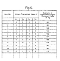
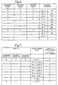
- Figure 5 shows an example of the contents of FIFO 306 after 11 lines of data.
- a microprocessor 308 calculates a set of seven decision thresholds for each of the combinations of preceding and succeeding levels and generates a look-up-table (LUT) which is stored in SRAM 312.
- samples 1-8 in the FIFO 306 represent the levels of the fourth symbol of the training data, T 3 , when both of the preceding symbols T 1 and T 2 and the succeeding symbol T 4 are at level 0.
- Figure 6 shows an example of the thresholds for this example case, as stored in the microprocessor's RAM, 310. The microprocessor then uses this set of thresholds to calculate a LUT, as shown in Figure 7, and stores it in SRAM, 312.
- the LUT is then used to perform thresholding of the valid data D in real time.
- the 8-bit input data is applied to the LUT 312, via input a.
- the previous two samples of the input data are input to inputs b and c respectively.
- the level of the subsequent sample of the input data is input via input d.
- This input d is a simple high/low indication derived from the sample before the one presented to input a of the comparator 312.
- the succeeding sample may have any value between the maximum and the minimum (213 and 0 respectively in this embodiment).
- a notional threshold is set midway between the maximum and the minimum. If the value of the subsequent sample is above this threshold, the value of the subsequent sample is considered to be high; if the value is below, it is considered to be low.
- Inputs b and c can be taken as latched outputs from the LUT 312 as then they have been quantised and are only three bits each, reducing the required LUT size.
- the LUT comprises two banks of SRAM. Once the microprocessor has calculated a LUT and written it to the SRAM, it 'pages' that LUT into the real-time data path. It then performs the whole cycle again, capturing a new FIFO full of training data and recalculating a set of thresholds. These can be averaged with the previous set to reduce the effects of random noise and a new LUT calculated. This is then paged-in in place of the previous LUT. The process repeats like this as fast as the processor can perform the tasks. Thus the system adapts to the response of the communications link 40 and tracks any long term changes in the response.
- the microprocessor can use the samples stored in the FIFO 306 to measure the pulse response of the link.
- the pulse response may indicate that the level of any sample is more dependent on the subsequent sample rather than the sample two-previously, which may happen if the bandwidth of the communications link is low.
- the training sequence can then be sampled at its third symbol rather than its fourth and the input to the LUTs can be changed to input more bits of the subsequent sample rather than the two-previous sample.
- the processor would then have samples of all the combinations of previous and subsequent samples and could generate LUTs in a similar way.
- the thresholded 3-bit symbols are then inverse Gray coded and passed through the BCH FEC detector/corrector 314 which corrects any single bit errors in each 64 bit block.
- the data then passes through a rate conversion FIFO 316 and is re-clocked out by control 318 at a continuous 15.0 MHz. This is passed to an MPEG demultiplexer/decoder for decoding in a conventional manner.
Landscapes
- Engineering & Computer Science (AREA)
- Multimedia (AREA)
- Signal Processing (AREA)
- Dc Digital Transmission (AREA)
- Compression, Expansion, Code Conversion, And Decoders (AREA)
- Compression Or Coding Systems Of Tv Signals (AREA)
Priority Applications (1)
| Application Number | Priority Date | Filing Date | Title |
|---|---|---|---|
| EP97927275A EP0908050B1 (en) | 1996-06-25 | 1997-06-19 | Data transmission |
Applications Claiming Priority (4)
| Application Number | Priority Date | Filing Date | Title |
|---|---|---|---|
| EP96304675 | 1996-06-25 | ||
| EP96304675 | 1996-06-25 | ||
| EP97927275A EP0908050B1 (en) | 1996-06-25 | 1997-06-19 | Data transmission |
| PCT/GB1997/001660 WO1997050247A1 (en) | 1996-06-25 | 1997-06-19 | Data transmission |
Publications (2)
| Publication Number | Publication Date |
|---|---|
| EP0908050A1 EP0908050A1 (en) | 1999-04-14 |
| EP0908050B1 true EP0908050B1 (en) | 2004-04-14 |
Family
ID=8224987
Family Applications (1)
| Application Number | Title | Priority Date | Filing Date |
|---|---|---|---|
| EP97927275A Expired - Lifetime EP0908050B1 (en) | 1996-06-25 | 1997-06-19 | Data transmission |
Country Status (9)
| Country | Link |
|---|---|
| EP (1) | EP0908050B1 (ja) |
| JP (1) | JP3841832B2 (ja) |
| CN (1) | CN1119021C (ja) |
| AU (1) | AU717303B2 (ja) |
| CA (1) | CA2258171C (ja) |
| DE (1) | DE69728668T2 (ja) |
| NO (1) | NO986108L (ja) |
| NZ (1) | NZ333254A (ja) |
| WO (1) | WO1997050247A1 (ja) |
Families Citing this family (2)
| Publication number | Priority date | Publication date | Assignee | Title |
|---|---|---|---|---|
| US6889351B1 (en) | 2000-03-30 | 2005-05-03 | Koninklijke Philips Electronics, N.V. | Backward compatible multiple data stream transmission method and system for compressed domain signals |
| DE10213872A1 (de) * | 2002-03-27 | 2003-10-16 | Siemens Ag | Verfahren zur verbesserten Datenübertragung in einem Übertragungssystem mit kombinierten Übertragungsformaten sowie zugehöriger Rahmenaufbau |
Citations (1)
| Publication number | Priority date | Publication date | Assignee | Title |
|---|---|---|---|---|
| US5287540A (en) * | 1991-11-01 | 1994-02-15 | Nokia Mobile Phones Ltd. | Digital detector |
Family Cites Families (3)
| Publication number | Priority date | Publication date | Assignee | Title |
|---|---|---|---|---|
| US4367488A (en) * | 1980-12-08 | 1983-01-04 | Sterling Television Presentations Inc. Video Data Systems Division | Data encoding for television |
| JPS60206390A (ja) * | 1984-03-30 | 1985-10-17 | Pioneer Electronic Corp | デイジタルデ−タエラ−ブロツク検出表示装置 |
| US5255090A (en) * | 1991-11-19 | 1993-10-19 | Scientific-Atlanta, Inc. | Progressive transmission of vector quantized data |
-
1997
- 1997-06-19 NZ NZ333254A patent/NZ333254A/xx not_active IP Right Cessation
- 1997-06-19 CA CA002258171A patent/CA2258171C/en not_active Expired - Fee Related
- 1997-06-19 AU AU31826/97A patent/AU717303B2/en not_active Ceased
- 1997-06-19 WO PCT/GB1997/001660 patent/WO1997050247A1/en active IP Right Grant
- 1997-06-19 CN CN97195871A patent/CN1119021C/zh not_active Expired - Fee Related
- 1997-06-19 EP EP97927275A patent/EP0908050B1/en not_active Expired - Lifetime
- 1997-06-19 JP JP50252098A patent/JP3841832B2/ja not_active Expired - Lifetime
- 1997-06-19 DE DE69728668T patent/DE69728668T2/de not_active Expired - Lifetime
-
1998
- 1998-12-23 NO NO986108A patent/NO986108L/no not_active Application Discontinuation
Patent Citations (1)
| Publication number | Priority date | Publication date | Assignee | Title |
|---|---|---|---|---|
| US5287540A (en) * | 1991-11-01 | 1994-02-15 | Nokia Mobile Phones Ltd. | Digital detector |
Also Published As
| Publication number | Publication date |
|---|---|
| NO986108D0 (no) | 1998-12-23 |
| CN1119021C (zh) | 2003-08-20 |
| CN1223769A (zh) | 1999-07-21 |
| NZ333254A (en) | 2000-04-28 |
| DE69728668D1 (de) | 2004-05-19 |
| JP3841832B2 (ja) | 2006-11-08 |
| AU3182697A (en) | 1998-01-14 |
| JP2001502478A (ja) | 2001-02-20 |
| DE69728668T2 (de) | 2005-03-17 |
| NO986108L (no) | 1998-12-23 |
| AU717303B2 (en) | 2000-03-23 |
| EP0908050A1 (en) | 1999-04-14 |
| WO1997050247A1 (en) | 1997-12-31 |
| CA2258171C (en) | 2005-05-17 |
| CA2258171A1 (en) | 1997-12-31 |
Similar Documents
| Publication | Publication Date | Title |
|---|---|---|
| US6094461A (en) | Data transmission | |
| US5121205A (en) | Apparatus for synchronizing main and auxiliary video signals | |
| US5602595A (en) | ATV/MPEG sync system | |
| US5497205A (en) | Apparatus for processing BPSK signal transmitted with NTSC TV on quadrature-phase video | |
| US5555024A (en) | Transmitters for burying digital signals within the trace and retrace intervals of NTSC television signals | |
| JP2837104B2 (ja) | ディジタル情報を伝送する装置及びディジタル信号受信器 | |
| US6687310B1 (en) | Trellis coded modulation system for digital television signal with trellis coded data and synchronization symbols | |
| JP3258022B2 (ja) | 可変サイズデータ配列のためのデータ・フレーム・フォーマット | |
| US6621426B1 (en) | Method and apparatus for modulating a signal | |
| US4541008A (en) | Television signal bandwidth reduction using variable rate transmission | |
| US6608870B1 (en) | Data frame for 8 MHZ channels | |
| JPH09511881A (ja) | 多レベルvsb伝送システムのためのデータレベル選択 | |
| Abbott | A differential pulse-code-modulation codec for videotelephony using four bits per sample | |
| EP0908050B1 (en) | Data transmission | |
| KR100481799B1 (ko) | 데이터전송시스템 | |
| CA2296146A1 (en) | Method and system for transmitting and decoding data in a signal | |
| US5410569A (en) | Data slicing system for HDTV receiver | |
| JPH08223229A (ja) | ベースバンド伝送システムおよび送信装置ならびに受信装置 | |
| EP0546628B1 (en) | Extended television system | |
| US6037992A (en) | Audio transmission in the video stream with adaptive gain | |
| JP3421711B2 (ja) | 標本化クロック再生システムおよび装置 | |
| JPH02170688A (ja) | 多重伝送方法およびその信号発生装置ならびにその信号再生装置 | |
| JPH10290437A (ja) | 映像信号のデジタル伝送方式 | |
| Underwood | Broadcast-Quality Television 45 MBIT/SEC (DS3) Encoding Algorithm | |
| Sun et al. | An ADPCM Receiver for NTSC Composite Video Signals |
Legal Events
| Date | Code | Title | Description |
|---|---|---|---|
| PUAI | Public reference made under article 153(3) epc to a published international application that has entered the european phase |
Free format text: ORIGINAL CODE: 0009012 |
|
| 17P | Request for examination filed |
Effective date: 19981207 |
|
| AK | Designated contracting states |
Kind code of ref document: A1 Designated state(s): BE DE DK ES FI FR GB IE IT NL PT SE |
|
| 17Q | First examination report despatched |
Effective date: 20030205 |
|
| GRAP | Despatch of communication of intention to grant a patent |
Free format text: ORIGINAL CODE: EPIDOSNIGR1 |
|
| GRAS | Grant fee paid |
Free format text: ORIGINAL CODE: EPIDOSNIGR3 |
|
| GRAA | (expected) grant |
Free format text: ORIGINAL CODE: 0009210 |
|
| AK | Designated contracting states |
Kind code of ref document: B1 Designated state(s): BE DE DK ES FI FR GB IE IT NL PT SE |
|
| PG25 | Lapsed in a contracting state [announced via postgrant information from national office to epo] |
Ref country code: NL Free format text: LAPSE BECAUSE OF FAILURE TO SUBMIT A TRANSLATION OF THE DESCRIPTION OR TO PAY THE FEE WITHIN THE PRESCRIBED TIME-LIMIT Effective date: 20040414 Ref country code: IT Free format text: LAPSE BECAUSE OF FAILURE TO SUBMIT A TRANSLATION OF THE DESCRIPTION OR TO PAY THE FEE WITHIN THE PRESCRIBED TIME-LIMIT;WARNING: LAPSES OF ITALIAN PATENTS WITH EFFECTIVE DATE BEFORE 2007 MAY HAVE OCCURRED AT ANY TIME BEFORE 2007. THE CORRECT EFFECTIVE DATE MAY BE DIFFERENT FROM THE ONE RECORDED. Effective date: 20040414 Ref country code: FI Free format text: LAPSE BECAUSE OF FAILURE TO SUBMIT A TRANSLATION OF THE DESCRIPTION OR TO PAY THE FEE WITHIN THE PRESCRIBED TIME-LIMIT Effective date: 20040414 Ref country code: BE Free format text: LAPSE BECAUSE OF FAILURE TO SUBMIT A TRANSLATION OF THE DESCRIPTION OR TO PAY THE FEE WITHIN THE PRESCRIBED TIME-LIMIT Effective date: 20040414 |
|
| REG | Reference to a national code |
Ref country code: GB Ref legal event code: FG4D |
|
| REF | Corresponds to: |
Ref document number: 69728668 Country of ref document: DE Date of ref document: 20040519 Kind code of ref document: P |
|
| REG | Reference to a national code |
Ref country code: IE Ref legal event code: FG4D |
|
| PG25 | Lapsed in a contracting state [announced via postgrant information from national office to epo] |
Ref country code: IE Free format text: LAPSE BECAUSE OF NON-PAYMENT OF DUE FEES Effective date: 20040621 |
|
| PG25 | Lapsed in a contracting state [announced via postgrant information from national office to epo] |
Ref country code: SE Free format text: LAPSE BECAUSE OF FAILURE TO SUBMIT A TRANSLATION OF THE DESCRIPTION OR TO PAY THE FEE WITHIN THE PRESCRIBED TIME-LIMIT Effective date: 20040714 Ref country code: DK Free format text: LAPSE BECAUSE OF FAILURE TO SUBMIT A TRANSLATION OF THE DESCRIPTION OR TO PAY THE FEE WITHIN THE PRESCRIBED TIME-LIMIT Effective date: 20040714 |
|
| PG25 | Lapsed in a contracting state [announced via postgrant information from national office to epo] |
Ref country code: ES Free format text: LAPSE BECAUSE OF FAILURE TO SUBMIT A TRANSLATION OF THE DESCRIPTION OR TO PAY THE FEE WITHIN THE PRESCRIBED TIME-LIMIT Effective date: 20040725 |
|
| NLV1 | Nl: lapsed or annulled due to failure to fulfill the requirements of art. 29p and 29m of the patents act | ||
| ET | Fr: translation filed | ||
| PLBE | No opposition filed within time limit |
Free format text: ORIGINAL CODE: 0009261 |
|
| STAA | Information on the status of an ep patent application or granted ep patent |
Free format text: STATUS: NO OPPOSITION FILED WITHIN TIME LIMIT |
|
| 26N | No opposition filed |
Effective date: 20050117 |
|
| REG | Reference to a national code |
Ref country code: IE Ref legal event code: MM4A |
|
| REG | Reference to a national code |
Ref country code: HK Ref legal event code: WD Ref document number: 1019380 Country of ref document: HK |
|
| PG25 | Lapsed in a contracting state [announced via postgrant information from national office to epo] |
Ref country code: PT Free format text: LAPSE BECAUSE OF NON-PAYMENT OF DUE FEES Effective date: 20040914 |
|
| PGFP | Annual fee paid to national office [announced via postgrant information from national office to epo] |
Ref country code: FR Payment date: 20110630 Year of fee payment: 15 |
|
| PGFP | Annual fee paid to national office [announced via postgrant information from national office to epo] |
Ref country code: DE Payment date: 20110622 Year of fee payment: 15 |
|
| REG | Reference to a national code |
Ref country code: FR Ref legal event code: ST Effective date: 20130228 |
|
| REG | Reference to a national code |
Ref country code: DE Ref legal event code: R119 Ref document number: 69728668 Country of ref document: DE Effective date: 20130101 |
|
| PG25 | Lapsed in a contracting state [announced via postgrant information from national office to epo] |
Ref country code: DE Free format text: LAPSE BECAUSE OF NON-PAYMENT OF DUE FEES Effective date: 20130101 Ref country code: FR Free format text: LAPSE BECAUSE OF NON-PAYMENT OF DUE FEES Effective date: 20120702 |
|
| PGFP | Annual fee paid to national office [announced via postgrant information from national office to epo] |
Ref country code: GB Payment date: 20160621 Year of fee payment: 20 |
|
| REG | Reference to a national code |
Ref country code: GB Ref legal event code: PE20 Expiry date: 20170618 |
|
| PG25 | Lapsed in a contracting state [announced via postgrant information from national office to epo] |
Ref country code: GB Free format text: LAPSE BECAUSE OF EXPIRATION OF PROTECTION Effective date: 20170618 |