EP0907261A2 - Signalwellenform Entzerrungsgerät - Google Patents
Signalwellenform Entzerrungsgerät Download PDFInfo
- Publication number
- EP0907261A2 EP0907261A2 EP98118874A EP98118874A EP0907261A2 EP 0907261 A2 EP0907261 A2 EP 0907261A2 EP 98118874 A EP98118874 A EP 98118874A EP 98118874 A EP98118874 A EP 98118874A EP 0907261 A2 EP0907261 A2 EP 0907261A2
- Authority
- EP
- European Patent Office
- Prior art keywords
- block
- signal
- afc
- section
- apc
- Prior art date
- Legal status (The legal status is an assumption and is not a legal conclusion. Google has not performed a legal analysis and makes no representation as to the accuracy of the status listed.)
- Withdrawn
Links
Images





Classifications
-
- H—ELECTRICITY
- H04—ELECTRIC COMMUNICATION TECHNIQUE
- H04B—TRANSMISSION
- H04B7/00—Radio transmission systems, i.e. using radiation field
- H04B7/005—Control of transmission; Equalising
-
- H—ELECTRICITY
- H04—ELECTRIC COMMUNICATION TECHNIQUE
- H04L—TRANSMISSION OF DIGITAL INFORMATION, e.g. TELEGRAPHIC COMMUNICATION
- H04L25/00—Baseband systems
- H04L25/02—Details ; arrangements for supplying electrical power along data transmission lines
- H04L25/0202—Channel estimation
- H04L25/024—Channel estimation channel estimation algorithms
- H04L25/025—Channel estimation channel estimation algorithms using least-mean-square [LMS] method
-
- H—ELECTRICITY
- H04—ELECTRIC COMMUNICATION TECHNIQUE
- H04L—TRANSMISSION OF DIGITAL INFORMATION, e.g. TELEGRAPHIC COMMUNICATION
- H04L25/00—Baseband systems
- H04L25/02—Details ; arrangements for supplying electrical power along data transmission lines
- H04L25/03—Shaping networks in transmitter or receiver, e.g. adaptive shaping networks
- H04L25/03006—Arrangements for removing intersymbol interference
- H04L25/03178—Arrangements involving sequence estimation techniques
- H04L25/03248—Arrangements for operating in conjunction with other apparatus
- H04L25/03254—Operation with other circuitry for removing intersymbol interference
- H04L25/03267—Operation with other circuitry for removing intersymbol interference with decision feedback equalisers
-
- H—ELECTRICITY
- H04—ELECTRIC COMMUNICATION TECHNIQUE
- H04L—TRANSMISSION OF DIGITAL INFORMATION, e.g. TELEGRAPHIC COMMUNICATION
- H04L27/00—Modulated-carrier systems
- H04L27/0014—Carrier regulation
- H04L2027/0044—Control loops for carrier regulation
- H04L2027/0063—Elements of loops
- H04L2027/0065—Frequency error detectors
-
- H—ELECTRICITY
- H04—ELECTRIC COMMUNICATION TECHNIQUE
- H04L—TRANSMISSION OF DIGITAL INFORMATION, e.g. TELEGRAPHIC COMMUNICATION
- H04L27/00—Modulated-carrier systems
- H04L27/0014—Carrier regulation
- H04L2027/0044—Control loops for carrier regulation
- H04L2027/0063—Elements of loops
- H04L2027/0067—Phase error detectors
Definitions
- the present invention relates to a signal waveform equalizer apparatus used for a receiver unit in multivalued digital microwave communication.
- modulation/demodulation technique for digital microwave communication has tended to further increase the value thereof in order to utilize frequencies even more effectively.
- QPSK and 16 QAM modulation techniques but also 64 QAM and 256 QAM modulation techniques and so forth are adopted in some cases.
- an automatic adaptive equalizer for equalizing the signal, which has been received at a receiver unit through a transmission line, is provided.
- FIG. 13 is a block diagram illustrating a transmission line and an exemplary equalization system therefor.
- the quality of a signal which has been transmitted by a transmitter, is varied in accordance with the characteristics of a transmission line, noise is added thereto and then the signal with a deformed waveform is received.
- the transmitted signal is affected by a ghost signal, which is received at a delayed time because of the influence of reflected waves and the like, so as to have a distorted waveform.
- noise and the like cause phase and frequency errors in the signals. Affected by various complicated factors such as these, a signal having a different waveform than that of an originally transmitted signal is received by a receiver unit.
- an equalizer is inserted to be serially connected to a receiver at a stage preceding the receiver, thereby equalizing a received signal X 0 into a signal Z 0 preferred by the receiver. And then, in order to restore original carrier waves, auto frequency control (AFC) and auto phase control (APC) are performed for removing frequency and phase errors, respectively.
- AFC auto frequency control
- API auto phase control
- equalization may be performed by an equalizer having a characteristic inverse of the transfer function of the transmission line. However, if the noise reaches a certain level, the equalizer must be designed taking the noise into consideration. In actuality, the equalizer is made up of digital filters, and such an equalizer is called a "digital equalizer".
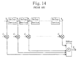
- FIG 14 is a block diagram illustrating an exemplary configuration for a digital filter.
- X 0 denotes a received signal input through the transmission line
- X 1 through X m are signals obtained by making respective delay devices delay the received signal X 0
- C 0 through C m denote respective equalization coefficients.
- the received signal X 0 is multiplied by the equalization coefficient C 0 by a multiplier.
- the signals X 1 through X m are respectively multiplied by the equalization coefficients C 1 through C m by respective multipliers.
- the products obtained by the respective multipliers are added by an adder and the sum is output as an equalized signal Z 0 .
- a component for multiplying a delayed signal by an associated equalization coefficient is called a "tap".
- the equalized signal Z 0 is obtained by adding the products obtained by the respective taps.
- optimum equalization coefficients C 0 through C m most suitable for restoring the original signal must be calculated.
- An least mean square (LMS) algorithm is ordinarily used for calculating the equalization coefficients.
- AFC/APC is implemented by a phase error detector, a loop filter and a digital VCO.
- an equalizer is made up of digital filters, complex multiplication is required. As the number of taps of the filter increases, the circuit size and the power consumption thereof also increase considerably. Also, in performing AFC/APC, a loop filter requires sum-of-products operations. Moreover, a digital VCO generally includes a means for storing data. Thus, if the number of bits of a signal is large, then the digital VCO requires an enormous storage capacity. From these points of view, it is an important problem to solve for a signal waveform equalizer apparatus to reduce the circuit size thereof.
- waveform equalization and AFC/APC cannot be completed in a single series of processing. Specifically, a signal, which has been subjected to AFC/APC, is fed back to the equalizer so as to equalize the waveform thereof again. Accordingly, waveform equalization and AFC/APC are repeatedly performed until the signal reaches and converges to a predetermined level. Ultimately, the signal is intended to be equalized and free from frequency and phase errors substantially simultaneously. In other words, the respective functions are not to be performed in such an independent manner that a signal is first equalized by waveform equalization and then errors are removed from the signal by AFC/APC.
- equalization and AFC/APC are so closely correlated processes that it is hard to draw fully satisfactory results therefrom if these processes are performed independently.
- AFC/APC are so closely correlated processes that it is hard to draw fully satisfactory results therefrom if these processes are performed independently.
- the object of this invention is providing a signal waveform equalizer apparatus of a reduced circuit size by integrating AFC/APC function with waveform equalization function.
- the present invention provides a signal waveform equalizer apparatus for equalizing the waveform of a signal, subjected to multivalued modulation and transmitted, with the waveform of an original signal yet to be transmitted.
- the apparatus includes: a waveform equalization section for equalizing the input modulated signal in accordance with a least mean square (LMS) algorithm; an error estimation block for producing error data required for the waveform equalization section to update equalization coefficients; and an auto frequency control (AFC)/auto phase control (APC) block for removing frequency and phase errors from the input modulated signal.
- the AFC/APC block removes the frequency and phase errors from the input modulated signal in accordance with the LMS algorithm and updates the coefficients by using the error data produced by the error estimation block.
- the signal waveform equalizer apparatus of the present invention includes: the waveform equalization section for equalizing the waveform of the modulated signal with the original one; and the AFC/APC block for removing frequency and phase errors from the modulated signal. And the AFC/APC block uses the error estimation block in common with the waveform equalization section. Accordingly, the function blocks implementing the waveform equalization and AFC/APC are not independent of each other, the AFC/APC function can be integrated into the signal waveform equalizer apparatus and the circuit size thereof can be considerably reduced.
- the waveform equalization section is preferably divided into an anterior stage and a posterior stage.
- the modulated signal, output from the anterior stage of the waveform equalization section, is preferably input to the AFC/APC block and an output signal of the AFC/APC block is preferably input to the posterior stage of the waveform equalization section.
- the anterior stage of the waveform equalization section is preferably a feed forward equalizer (FFE) block and the posterior stage of the waveform equalization section is preferably a decision feedback equalizer (DFE) block.
- FFE feed forward equalizer
- DFE decision feedback equalizer
- the FFE block preferably includes an FFE filter section that is divided into an FFE pre-filter and an FFE post-filter.
- the DFE block preferably includes a DFE filter section that is divided into a DFE pre-filter and a DFE post-filter.
- each of the FFE pre- and post-filters and the DFE pre- and post-filters preferably includes a complex operation macro having the same configuration.
- the present invention also provides another signal waveform equalizer apparatus for equalizing the waveform of a signal, which has been subjected to multivalued modulation and transmitted, with the waveform of an original signal yet to be transmitted.
- the apparatus includes: a waveform equalization section for equalizing the input modulated signal in accordance with an LMS algorithm; and an AFC/APC block for removing frequency and phase errors from the input modulated signal.
- the AFC/APC block includes a single tap for multiplying the input modulated signal by a coefficient for removing the frequency and phase errors, and an AFC/APC coefficient update section for updating the coefficient in accordance with the LMS algorithm.
- the signal waveform equalizer apparatus of the present invention includes: the waveform equalization section for equalizing the waveform of the modulated signal with the original one; and the AFC/APC block for removing frequency and phase errors from the modulated signal. And the AFC/APC block operates in accordance with the LMS algorithm in the same way as the waveform equalization section. Accordingly, since waveform equalization and AFC/APC can be implemented by similar components, the AFC/APC function can be integrated into the signal waveform equalizer apparatus and the circuit size thereof can be considerably reduced.
- the waveform equalization section is preferably divided into an anterior stage and a posterior stage, each of these stages including a filter section and a coefficient update section.
- the modulated signal, output from the anterior stage of the waveform equalization section, is preferably input to the AFC/APC block and an output signal of the AFC/APC block is preferably input to the posterior stage of the waveform equalization section.
- the filter sections of the anterior and posterior stages of the waveform equalization section preferably have the same number of taps.
- FIG. 1 is a block diagram illustrating a general configuration for the signal waveform equalizer apparatus of the present invention.
- the reference numeral 10 denotes a feed forward equalizer (FFE) block, which is the anterior stage of a waveform equalization section 1 for equalizing the waveform of a modulated signal.
- 20 denotes a decision feedback equalizer (DFE) block, which is the posterior stage of the waveform equalization section 1 .
- 30 denotes an error estimation block.
- 40 denotes an auto frequency control (AFC)/auto phase control (APC) block for removing frequency and phase errors from the modulated signal.
- the FFE block 10 includes an FFE coefficient update section 11 and an FFE filter section 12 .
- the DFE block 20 includes a DFE coefficient update section 21 and a DFE filter section 22 .
- the AFC/APC block 40 includes an AFC/APC coefficient update section 41 and a tap 42 .
- the signal waveform equalizer apparatus of the present invention shown in Figure 1 receives a modulated signal, which has been subjected to multivalued modulation and transmitted, converts the signal into an equalized signal and then outputs the equalized signal.
- the modulated signal received is equalized by the FFE block 10 , which is the anterior stage of the waveform equalization section 1 .
- the equalized signal is input to the AFC/APC block 40 , which removes frequency and phase errors from the signal.
- the modulated signal, output from the AFC/APC block 40 is further equalized by the DFE block 20 , which is the posterior stage of the waveform equalization section 1 . And then the signal is output as an equalized signal from the signal waveform equalizer apparatus.
- the waveform equalization section 1 and the AFC/APC block 40 both operate in accordance with an LMS algorithm and to update coefficients by using error data produced by the error estimation block 30 .
- the quality of a signal transmitted by a transmitter are varied in accordance with the characteristics of a transmission line. And the signal is provided to a receiver with noise added thereto. If the characteristics of the transmission line are constant, then characteristics inverse of those of the transmission line should be calculated and a constant equalization coefficient realizing the inverse characteristics calculated may be used. In a system in which the influence and characteristics of noise are varied perpetually, however, the equalization coefficient should be successively updated in accordance with the states of the received signal.
- a so-called "automatic adaptive algorithm” is used for updating the equalization coefficient. In actuality, a next equalization coefficient is calculated based on an equalization coefficient in a previous state. In such a case, a certain index of estimation is set and the equalization coefficient is updated so as to minimize the value.
- a least mean square (LMS) algorithm is a typical example of such an algorithm.
- the original signal ⁇ 0 yet to be transmitted is unknown to a receiver unit, the original signal cannot be used for calculating the error data e 0 .
- Such an algorithm is called a "blind algorithm”. If an equalization coefficient is repeatedly updated several thousand times under some constraint in accordance with the blind algorithm, then the equalization coefficient converges, thereby realizing equalization of the signal waveform.
- Figure 11 is a diagram illustrating the first quadrant of a 64 QAM phase diagram and showing the relationship between an LMS error and a Sato error.
- solid circles represent the positions of signal points and the circled solid circle represent the reference point of the Sato error.
- the equalized signal Z 0 is located at the position represented by the open circle in Figure 11
- the LMS error and the Sato error are represented by respective vectors shown in Figure 11 .
- the reference point of the Sato error exists in each quadrant. That is to say, there are four reference points for the Sato error.
- the reference points of the LMS error are located at the respective signal points.
- 64 QAM there are 64 reference points in total for the LMS error.
- the waveform equalizer of the present invention updates the equalization coefficient in accordance with Equations (6) and (7).
- the AFC/APC block 40 performs the frequency correction and the phase correction in accordance with the LMS algorithm, too.
- Equation (8) (D n - H n U n ) is equivalent to the error data in the STOP & GO algorithm for obtaining the equalization coefficient, which may be the error data output from the error estimation block 30 .
- H n U n A signal, from which errors have been removed, is represented by H n U n .
- H n U n is a signal in which both the phase and frequency errors have been corrected.
- FIG. 2 is a diagram illustrating a configuration for a signal waveform equalizer apparatus in the first embodiment of the present invention.
- an FFE filter section 12 includes: a number (m+1)(where m is a positive integer) of taps; delay devices; and an adder.
- Equalization coefficients C f0 through C fm updated by an FFE coefficient update section 11 are provided to the respective taps.
- a DFE filter section 22 includes: a slicer 25 ; a number (m+1) of taps; delay devices; and an adder.
- Equalization coefficients C d0 through C dm updated by a DFE coefficient update section 21 are provided to the respective taps.
- the error data Err produced by the error estimation block 30 is input to the FFE coefficient update section 11 , the DFE coefficient update section 21 and the AFC/APC coefficient update section 41 and used for updating the respective coefficients.
- the AFC/APC block 40 is disposed just at the center of the waveform equalization section 1 . That is to say, the number of taps of the FFE block 10 as the anterior stage of the waveform equalization section 1 is equal to the number of taps of the DFE block 20 as the posterior stage thereof.
- This arrangement is employed to simplify the circuit configuration and thereby reduce the resulting circuit size. In addition, it was also found that such a configuration also enhances the performance.
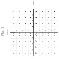
- Figure 3 is a constellation obtained by performing a simulation in this embodiment.
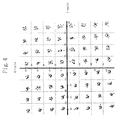
- Figure 4 is also a constellation, obtained by performing a simulation, of a comparative example, in which an AFC/APC block is disposed posterior to the overall waveform equalization section 1 .
- equalized signals are more concentrated about the position of a corresponding signal point in the constellation shown in Figure 3 than in the constellation shown in Figure 4 .
- this embodiment is superior in performance to the comparative example.
- the FFE filter section 12 and the DFE filter section 22 of the signal waveform equalizer apparatus shown in Figure 1 are each divided into a pre-filter and a post-filter, and each filter has a complex operation section having the same configuration.
- the signal waveform equalizer apparatus of the second embodiment will be described in detail.
- the number of taps of a filter is assumed to be eight.
- Figure 5 is a diagram illustrating a configuration for the FFE filter section 12 of the signal waveform equalizer apparatus of the second embodiment.
- the reference numerals 50A and 50B denote complex operation sections implemented by complex operation macros to be described in detail later.
- 51a and 51b denote respective banks of data holders for sequentially holding real parts of modulated signals.
- 52a and 52b denote respective banks of data holders for sequentially holding imaginary parts of the modulated signals.
- 53a and 53b denote respective banks of data holders for sequentially holding tap coefficients.
- 54a and 54c denote respective adders for calculating real parts.
- 55a and 55c denote respective adders for calculating imaginary parts.
- And 54b, 54d, 55b and 55d denote respective data holders.
- the banks of data holders 51a, 52a and 53a and the complex operation section 50A constitute an FFE pre-filter 12a .
- the banks of data holders 51b, 52b and 53b, the complex operation section 50B, the adders 54a, 54c, 55a, 55c and the data holders 54b, 54d, 55b, 55d constitute an FFE post-filter 12b .
- the banks 51a and 52a of data holders respectively hold the real parts and the imaginary parts of modulated signals, which have been subjected to multivalued modulation and then externally transmitted sequentially.
- the bank 53a of data holders holds the tap coefficients produced and output by the FFE coefficient update section 11 .
- the tap coefficient is transferred at a rate twice as high as the rate at which the modulated signal is transferred.
- the bank 53a of data holders is formed to serially transfer the real parts and imaginary parts of the tap coefficients.
- the complex operation section 50A performs a complex operation by using the real and imaginary parts of the four modulated signals held in the banks 51a and 52a of data holders and the real and imaginary parts of the four tap coefficients held in the bank 53a of data holders and by selecting appropriate data.
- the complex operation section 50A outputs a real part DRa and an imaginary part DIa as the results of operation to the FFE post-filter 12b .
- the banks 51b and 52b of data holders respectively hold the real and imaginary parts of the modulated signals, which are once held in the banks 51a and 52a of data holders of the FFE pre-filter 12a and then output therefrom.
- the bank 53b of data holders holds the tap coefficients which are once held in the bank 53a of data holders of the FFE pre-filter 12a and then output therefrom.
- the tap coefficient is transferred at a rate twice as high as the rate at which the modulated signal is transferred.
- the bank 53b of data holders is formed to serially transfer the real and imaginary parts of the tap coefficients.
- the complex operation section 50B performs a complex operation by using the real and imaginary parts of the four modulated signals held in the banks 51b and 52b of data holders and the real and imaginary parts of the four tap coefficients held in the bank 53b of data holders and by selecting appropriate data.
- the complex operation section 50B outputs a real part DRb and an imaginary part DIb as the results of operation.
- the real part DRb obtained by the complex operation section 50B of the FFE post-filter 12b as the result of operation and the real part DRa obtained by the complex operation section 50A of the FFE pre-filter 12a as the result of operation are added together by the adder 54a . And the sum is retained in the holder 54b .
- the data retained in the holder 54b and the real part of an appropriate one of the modulated signals held in the bank 51b of data holders are added together by the adder 54c .
- the sum is retained in the holder 54d and then output as the real part of the resultant data of the FFE filter section 12 .
- the imaginary part DIb obtained by the complex operation section 50B of the FFE post-filter 12b as the result of operation and the imaginary part DIa obtained by the complex operation section 50A of the FFE pre-filter 12a as the result of operation are added together by the adder 55a .
- the sum is retained in the holder 55b .
- the data retained in the holder 55b and the imaginary part of an appropriate one of the modulated signals held in the bank 52b of data holders are added together by the adder 55c .
- the sum is retained in the holder 55d and then output as the imaginary part of the resultant data of the FFE filter section 12 .
- FIG. 6 is a diagram illustrating a configuration for the DFE filter section 22 of the signal waveform equalizer apparatus of the second embodiment.
- the reference numerals 50C and 50D denote complex operation sections implemented by complex operation macros to be described in detail later.
- 60 denotes a slicer for converting a modulated signal, from which the frequency and phase errors have been removed by the AFC/APC block 40 , into a decision signal.
- 61a and 61b denote respective banks of data holders for sequentially holding real parts of the decision signals.
- 62a and 62b denote respective banks of data holders for sequentially holding imaginary parts of the decision signals.
- 63a and 63b denote respective banks of data holders for sequentially holding tap coefficients.
- 64a denotes an adder for calculating a real part.
- 65a denotes an adder for calculating an imaginary part.
- 64b , 64c , 65b and 65c denote respective data holders.
- the slicer 60 , the banks 61a, 62a and 63a of data holders and the complex operation section 50C constitute a DFE pre-filter 22a .
- the banks 61b , 62b and 63b of data holders, the complex operation section 50D , the adders 64a and 65a and the data holders 64b , 64c , 65b , 65c constitute a DFE post-filter 22b .
- the banks 61a and 62a of data holders respectively retain the real parts and the imaginary parts of the decision signals.
- the bank 63a of data holders retains the tap coefficients produced and output by the DFE coefficient update section 21 .
- the tap coefficient is transferred at a rate twice as high as the rate at which the decision signal is transferred.
- the bank 63a of data holders is formed to serially transfer the real and imaginary parts of the tap coefficients.
- the complex operation section 50C performs a complex operation by using the real and imaginary parts of the four decision signals retained in the banks 61a and 62a of data holders and the real and imaginary parts of the four tap coefficients retained in the bank 63a of data holders and by selecting appropriate data.
- the complex operation section 50C outputs a real part DRc and an imaginary part DIc as the results of operation to the DFE post-filter 22b .
- the banks 61b and 62b of data holders respectively retain the real and imaginary parts of the decision signals, which are once retained in the banks 61a and 62a of data holders of the DFE pre-filter 22a and then output therefrom.
- the bank 63b of data holders retains the tap coefficients which are once retained in the bank 63a of data holders of the DFE pre-filter 22a and then output therefrom.
- the tap coefficient is transferred at a rate twice as high as the rate at which the decision signal is transferred.
- the bank 63b of data holders is formed to serially transfer the real and imaginary parts of the tap coefficients.
- the complex operation section 50D performs a complex operation by using the real and imaginary parts of the four decision signals retained in the banks 61b and 62b of data holders and the real and imaginary parts of the four tap coefficients retained in the bank 63b of data holders and by selecting appropriate data.
- the complex operation section 50D outputs a real part DRd and an imaginary part DId as the results of operation.
- the real part DRd obtained by the complex operation section 50D of the DFE post-filter 22b as the result of operation and the real part DRc obtained by the complex operation section 50C of the DFE pre-filter 22a as the result of operation are added together by the adder 64a . And the sum is retained in the holder 64b . The data retained in the holder 64b is further retained in the holder 64c and then output as the real part of the resultant data of the DFE filter section 22 . Similarly, the imaginary part DId obtained by the complex operation section 50D of the DFE post-filter 22b as the result of operation and the imaginary part DIc obtained by the complex operation section 50C of the DFE pre-filter 22a as the result of operation are added together by the adder 65a . And the sum is retained in the holder 65b . The data retained in the holder 65b is further retained in the holder 65c and then output as the imaginary part of the resultant data of the DFE filter section 22 .
- FIG 7 is a diagram illustrating a configuration for a complex operation macro used in this embodiment.
- This complex operation macro performs multiplexing and complex multiplication on the tap coefficients for four taps and modulated signals to be equalized, and is used as the complex operation section 50A , 50B of the FFE filter section 12 shown in Figure 5 and as the complex operation section 50C , 50D of the DFE filter section 22 shown in Figure 6 .
- the reference numerals 101a through 101d and 103a through 103d denote selectors
- 102a through 102d and 104a through 104d denote data holders.
- the real parts of the tap coefficients for four taps are input in parallel to each other, serially converted by the selectors 101a through 101d and the data holders 102a through 102d into a real part for one tap and then output as a serial output c from the data holder 102d .
- the imaginary parts of the tap coefficients for four taps are input in parallel to each other, serially converted by the selectors 103a through 103d and the data holders 104a through 104d into an imaginary part for one tap and then output as a serial output d from the data holder 104d .
- the serial outputs c and d are input to the selectors 101a and 103a , respectively. That is to say, both the real and imaginary parts of a tap coefficient have cyclic data.
- data for one tap is selected at an appropriate time by the selector 105 from the real parts of the four modulated signals to be equalized and is output as a real part a .
- data for one tap is selected at an appropriate time by the selector 106 from the imaginary parts of the four modulated signals to be equalized and is output as an imaginary part b .
- a multiplier 107a calculates ac in this equation and a multiplier 107b calculates bd in this equation.
- a multiplier 108a calculates ad in this equation and a multiplier 108b calculates bc in this equation.
- a subtracter 107c subtracts bd calculated by the multiplier 107b from ac calculated by the multiplier 107a , thereby obtaining (ac - bd) as a real part in the complex operation.
- an adder 108c adds together ad calculated by the multiplier 108a and bc calculated by the multiplier 108b , thereby obtaining (ad + bc) as an imaginary part in the complex operation.
- An adder 107d adds together the real part (ac - bd) calculated by the subtracter 107c and the data retained in a data holder 107e and the sum is held in the data holder 107e .
- an adder 108d adds together the imaginary part (ad + bc) calculated by the adder 108c and the data retained in a data holder 108e and the sum is held in the data holder 108e .
- the adders 107d and 108d and the data holders 107e and 108e sequentially add together these real and imaginary parts, thereby outputting resultant real and imaginary parts for four taps.
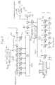
- FIG 8 is a diagram illustrating a configuration for the FFE coefficient update section 11 of the signal waveform equalizer apparatus in this embodiment.
- the FFE coefficient update section 11 calculates the coefficient to be updated basically in accordance with the STOP & GO algorithm as represented by Equations (6) and (7).
- a complex multiplication of anti-rotation data is additionally performed. That is to say, the FFE coefficient update section 11 shown in Figure 8 has a circuit configuration in which the coefficient update processing as represented by Equations (6) and (7) and complex multiplication processing of anti-rotation data are multiplexed.
- a selector 71a selectively outputs the sine or cosine component of the anti-rotation data that has been output by the AFC/APC block 40 to remove errors from the phase and frequency components.
- a selector 71b selectively outputs the real or imaginary part of the error data output from the error estimation block 30 .
- a selector 71c selectively outputs the real or imaginary part of the modulated signal that has been retained and then output at an appropriate time by the FFE filter section 12 .
- the real or imaginary part of the error data selectively output by the selector 71b and the real or imaginary part of the modulated signal selectively output by the selector 71c are multiplied together by a multiplier 72 . And the product is input to a sum-of-products calculator 73 .
- the sum-of-products calculator 73 multiplies together the sine or cosine component of the anti-rotation data selectively output by the selector 71a and the product obtained by the multiplier 72 , and adds the sum of products, which is retained in a data holder 74 , to this product, thereby outputting a new sum of products. This new sum of products is also retained in the data holder 74 .
- the multiplication of the step parameter ⁇ in Equations (6) and (7) is performed.
- the multiplication of the step parameter ⁇ is performed by bit shifting.
- the reference numerals 75a , 75b and 75c denote bit shifters for multiplying the step parameters ⁇ 1 , ⁇ 2 and ⁇ 3 , respectively, and 76a , 76b and 76c denote selectors.
- the selector 76a selectively outputs the sum of products output by the sum-of-products calculator 73 , or the data obtained by the bit shifter 75a multiplying the sum of products by ⁇ 1 .
- the selector 76b selectively outputs the output data of the selector 76a , or the data obtained by the bit shifter 75b multiplying the output data by ⁇ 2 .
- the selector 76c selectively outputs the output data of the selector 76b , or the data obtained by the bit shifter 75c multiplying the output data by ⁇ 3 .
- the output data of the selector 76c is added by an adder 77 to the tap coefficient that has been retained and then output at an appropriate time by the FFE filter section 12 .
- the sum is the newly updated tap coefficient, which is retained in a holder 78 and then output as a new tap coefficient.
- FIG. 9 is a diagram illustrating a configuration for the DFE coefficient update section 21 of the signal waveform equalizer apparatus in this embodiment.
- the DFE coefficient update section 21 calculates the coefficient to be updated basically in accordance with the STOP & GO algorithm as represented by Equations (6) and (7).
- the DFE coefficient update section 21 shown in Figure 9 updates the coefficient of the DFE block 20 .
- the decision signal obtained as a result of processing by the FFE block 10 and the AFC/APC block 40 , is input to the DFE coefficient update section 21 .
- the DFE coefficient update section 21 has a circuit configuration in which the coefficient update processing and complex multiplication processing on this decision signal and the error data are multiplexed.
- a selector 81a selectively outputs the real or imaginary part of the decision signal that has been retained and then output at an appropriate time by the DFE filter section 22 .
- a selector 81b selectively outputs the real or imaginary part of the error data output from the error estimation block 30 .
- a sum-of-products calculator 82 multiplies together the real or imaginary part of the decision signal selectively output by the selector 81a and the real or imaginary part of the error data selectively output by the selector 81b , and adds the sum of products, which is retained in a data holder 83 , to this product, thereby outputting a new sum of products. This new sum of products is also retained in the data holder 83 .
- the multiplication of the step parameter ⁇ in Equations (6) and (7) is performed.
- the multiplication of the step parameter ⁇ is performed by bit shifting as in the FFE coefficient update section 11 shown in Figure 8 .
- the reference numerals 84a , 84b and 84c denote bit shifters for multiplying the step parameters ⁇ 1 , ⁇ 2 and ⁇ 3 , respectively, and 85a , 85b and 85c denote selectors.
- the selector 85a selectively outputs the sum of products output by the sum-of-products calculator 82 , or the data obtained by the bit shifter 84a multiplying the sum of products by ⁇ 1 .
- the selector 85b selectively outputs the output data of the selector 85a , or the data obtained by the bit shifter 84b multiplying the output data by ⁇ 2 .
- the selector 85c selectively outputs the output data of the selector 85b , or the data obtained by the bit shifter 84c multiplying the output data by ⁇ 3 .
- the output data of the selector 85c is added by an adder 86 to the tap coefficient that has been retained and then output at an appropriate time by the DFE filter section 22 .
- the sum is the newly updated tap coefficient, which is once retained in a holder 87 and then output as a new tap coefficient.
- FIG 10 is a diagram illustrating a configuration for the AFC/APC coefficient update section 41 of the signal waveform equalizer apparatus in this embodiment.
- the AFC/APC coefficient update section 41 calculates the coefficient to be updated basically in accordance with the LMS algorithm as represented by Equations (8) and (9).
- a complex multiplier 91a performs a complex multiplication on the real and imaginary parts of the error data and the real and imaginary parts of the modulated signal output from the FFE filter section 12 . This product is further multiplied by the step size represented by Equation (8).
- the multiplication of the step size is performed by bit shifting and the values that can be multiplied by bit shifting are defined as step sizes.
- a bit shifter 91b multiplies together the product obtained by the complex multiplier 91a and a step size.
- a complex multiplier 93 performs a complex multiplication on the real and imaginary parts of a frequency correction coefficient yet to be updated and the real and imaginary parts of a phase correction coefficient yet to be updated and then outputs the product.
- Equation (8) the operation represented by Equation (8) is realized.
- a holder 91d retains the output data of the adder 91c , i.e., the phase correction coefficient, and then outputs the real and imaginary parts thereof.
- This phase correction coefficient is used as a phase correction coefficient yet to be updated, which is required for performing the next operation in accordance with Equation (8).
- Equation (9) F n + ⁇ f ⁇ ⁇ (D n - H n U n )U n *H n *
- a complex multiplier 92a performs a complex multiplication on the real and imaginary parts of the error data and the real and imaginary parts of the modulated signal, which is the product obtained by the complex multiplier (tap) 42 .
- the multiplication of a step size is performed by bit shifting as in the operation to update the phase correction coefficient in accordance with Equation (8).
- a bit shifter 92b multiplies together the product obtained by the complex multiplier 92a and a step size.
- Equation (10) the operation represented by Equation (10) is realized.
- the holder 92d retains the output data of the adder 92c , i.e., the frequency correction coefficient, and then outputs the real and imaginary parts thereof.
- This frequency correction coefficient is used as a frequency correction coefficient yet to be updated, which is required for performing the next operation in accordance with Equation (10).
- the signal waveform equalizer apparatus of the present invention includes a waveform equalization section for equalizing the waveform of a modulated signal and an AFC/APC block for removing the frequency and phase errors from the modulated signal.
- the AFC/APC block operates in accordance with the LMS algorithm as the waveform equalization section does.
- the AFC/APC block can be implemented by a tap and a coefficient update section that have the same function as that of the waveform equalization section.
- the AFC/APC block uses an error estimation block in common with the waveform equalization section.
- the AFC/APC function can be integrated into the signal waveform equalizer apparatus and the circuit size thereof can be reduced considerably.
Landscapes
- Engineering & Computer Science (AREA)
- Computer Networks & Wireless Communication (AREA)
- Signal Processing (AREA)
- Power Engineering (AREA)
- Digital Transmission Methods That Use Modulated Carrier Waves (AREA)
- Cable Transmission Systems, Equalization Of Radio And Reduction Of Echo (AREA)
- Filters That Use Time-Delay Elements (AREA)
Applications Claiming Priority (3)
| Application Number | Priority Date | Filing Date | Title |
|---|---|---|---|
| JP274073/97 | 1997-10-07 | ||
| JP27407397 | 1997-10-07 | ||
| JP27407397A JP3865482B2 (ja) | 1997-10-07 | 1997-10-07 | 信号波形等化装置 |
Publications (2)
| Publication Number | Publication Date |
|---|---|
| EP0907261A2 true EP0907261A2 (de) | 1999-04-07 |
| EP0907261A3 EP0907261A3 (de) | 2001-10-04 |
Family
ID=17536604
Family Applications (1)
| Application Number | Title | Priority Date | Filing Date |
|---|---|---|---|
| EP98118874A Withdrawn EP0907261A3 (de) | 1997-10-07 | 1998-10-06 | Signalwellenform Entzerrungsgerät |
Country Status (5)
| Country | Link |
|---|---|
| US (1) | US6421378B1 (de) |
| EP (1) | EP0907261A3 (de) |
| JP (1) | JP3865482B2 (de) |
| KR (1) | KR100538601B1 (de) |
| CN (1) | CN1131604C (de) |
Cited By (2)
| Publication number | Priority date | Publication date | Assignee | Title |
|---|---|---|---|---|
| EP1115236A3 (de) * | 2000-01-04 | 2003-12-17 | Alcatel Internetworking, Inc. | Entzerrung für einen Mehrkanal-Empfangsknoten |
| US6907064B1 (en) | 1999-10-29 | 2005-06-14 | Matsushita Electric Industrial Co., Ltd. | Waveform equalization controller and waveform equalization control method |
Families Citing this family (25)
| Publication number | Priority date | Publication date | Assignee | Title |
|---|---|---|---|---|
| JP3560138B2 (ja) * | 1999-12-06 | 2004-09-02 | 松下電器産業株式会社 | 波形等化器とこれを用いた移動局無線装置、基地局無線装置及び移動通信システム |
| KR100320214B1 (ko) * | 2000-02-12 | 2002-01-10 | 구자홍 | 채널 등화기 |
| US7072392B2 (en) * | 2000-11-13 | 2006-07-04 | Micronas Semiconductors, Inc. | Equalizer for time domain signal processing |
| US6940557B2 (en) | 2001-02-08 | 2005-09-06 | Micronas Semiconductors, Inc. | Adaptive interlace-to-progressive scan conversion algorithm |
| US6829297B2 (en) * | 2001-06-06 | 2004-12-07 | Micronas Semiconductors, Inc. | Adaptive equalizer having a variable step size influenced by output from a trellis decoder |
| US7190744B2 (en) * | 2001-06-07 | 2007-03-13 | Micronas Semiconductors, Inc. | Error generation for adaptive equalizer |
| US7418034B2 (en) * | 2001-06-19 | 2008-08-26 | Micronas Semiconductors. Inc. | Combined trellis decoder and decision feedback equalizer |
| US7017104B1 (en) * | 2001-08-24 | 2006-03-21 | Mediatek Inc. | Method and system for decoding block codes by calculating a path metric according to a decision feedback sequence estimation algorithm |
| US7173966B2 (en) * | 2001-08-31 | 2007-02-06 | Broadband Physics, Inc. | Compensation for non-linear distortion in a modem receiver |
| US20030206053A1 (en) * | 2002-04-04 | 2003-11-06 | Jingsong Xia | Carrier recovery for DTV receivers |
| US20030235259A1 (en) * | 2002-04-04 | 2003-12-25 | Jingsong Xia | System and method for symbol clock recovery |
| US6980059B2 (en) * | 2002-04-05 | 2005-12-27 | Micronas Semiconductors, Inc. | Data directed frequency acquisition loop that synchronizes to a received signal by using the redundancy of the data in the frequency domain |
| US7272203B2 (en) * | 2002-04-05 | 2007-09-18 | Micronas Semiconductors, Inc. | Data-directed frequency-and-phase lock loop for decoding an offset-QAM modulated signal having a pilot |
| US7376181B2 (en) * | 2002-04-05 | 2008-05-20 | Micronas Semiconductors, Inc. | Transposed structure for a decision feedback equalizer combined with a trellis decoder |
| US6995617B2 (en) * | 2002-04-05 | 2006-02-07 | Micronas Semiconductors, Inc. | Data-directed frequency-and-phase lock loop |
| US7321642B2 (en) * | 2002-04-05 | 2008-01-22 | Micronas Semiconductors, Inc. | Synchronization symbol re-insertion for a decision feedback equalizer combined with a trellis decoder |
| KR100518029B1 (ko) * | 2002-06-11 | 2005-10-04 | 한국전자통신연구원 | 블라인드 판정궤환등화 장치 및 그 방법 |
| KR100480881B1 (ko) * | 2002-06-27 | 2005-04-07 | 학교법인대우학원 | 에러궤환을 이용한 블라인드 적응결정 궤환 등화기 |
| KR100556387B1 (ko) * | 2003-10-20 | 2006-03-03 | 엘지전자 주식회사 | 시간영역 적응 등화 장치 및 그 방법 |
| US20050129148A1 (en) * | 2003-12-11 | 2005-06-16 | Wideband Semiconductors, Inc. | Control algorithm in QAM modems |
| US7961782B2 (en) * | 2007-06-04 | 2011-06-14 | Infineon Technologies Ag | Interference suppression processing unit and a method of suppressing interference in wireless data communication |
| WO2010147891A2 (en) | 2009-06-14 | 2010-12-23 | Nulabel Technologies, Inc. | Liner-free label and systems |
| US8929429B2 (en) * | 2009-10-15 | 2015-01-06 | Hiroshi Takatori | Adaptive pade filter and transceiver |
| CN104780037B (zh) * | 2014-01-10 | 2019-04-30 | 深圳市中兴微电子技术有限公司 | 一种时钟恢复方法、装置及系统 |
| US11438197B2 (en) * | 2020-11-12 | 2022-09-06 | Texas Instruments Incorporated | Adaptive equalizer with a real feedforward filter and a single complex feedforward tap |
Family Cites Families (6)
| Publication number | Priority date | Publication date | Assignee | Title |
|---|---|---|---|---|
| US5297165A (en) * | 1990-07-06 | 1994-03-22 | Nippon Telegraph And Telephone Corporation | Equalizer for radio receive signal |
| JPH05219510A (ja) * | 1992-01-31 | 1993-08-27 | Sony Corp | ビデオ信号処理装置 |
| US5710792A (en) * | 1993-12-15 | 1998-01-20 | Ntt Mobile Communications Network, Inc. | Adaptive equalizer |
| US5796535A (en) * | 1995-05-12 | 1998-08-18 | Cirrus Logic, Inc. | Sampled amplitude read channel employing a user data frequency synthesizer and a servo data frequency synthesizer |
| EP1062444A4 (de) * | 1996-10-22 | 2001-04-11 | Kalsi Eng Inc | Flexibler keilschieber |
| US5966188A (en) * | 1996-12-26 | 1999-10-12 | Samsung Electronics Co., Ltd. | Decimation of baseband DTV signals prior to channel equalization in digital television signal receivers |
-
1997
- 1997-10-07 JP JP27407397A patent/JP3865482B2/ja not_active Expired - Fee Related
-
1998
- 1998-10-02 US US09/165,204 patent/US6421378B1/en not_active Expired - Lifetime
- 1998-10-06 EP EP98118874A patent/EP0907261A3/de not_active Withdrawn
- 1998-10-07 KR KR1019980041802A patent/KR100538601B1/ko not_active Expired - Fee Related
- 1998-10-07 CN CN98120126A patent/CN1131604C/zh not_active Expired - Fee Related
Non-Patent Citations (1)
| Title |
|---|
| FUKUOKA T ET AL: "AN AREA EFFECTIVE 1-CHIP QAM LSI FOR DIGITAL CATV" IEEE TRANSACTIONS ON CONSUMER ELECTRONICS, IEEE INC. NEW YORK, US, vol. 43, no. 3, 1 August 1997 (1997-08-01), pages 649-654, XP000742545 ISSN: 0098-3063 * |
Cited By (2)
| Publication number | Priority date | Publication date | Assignee | Title |
|---|---|---|---|---|
| US6907064B1 (en) | 1999-10-29 | 2005-06-14 | Matsushita Electric Industrial Co., Ltd. | Waveform equalization controller and waveform equalization control method |
| EP1115236A3 (de) * | 2000-01-04 | 2003-12-17 | Alcatel Internetworking, Inc. | Entzerrung für einen Mehrkanal-Empfangsknoten |
Also Published As
| Publication number | Publication date |
|---|---|
| JP3865482B2 (ja) | 2007-01-10 |
| CN1213906A (zh) | 1999-04-14 |
| KR19990036892A (ko) | 1999-05-25 |
| EP0907261A3 (de) | 2001-10-04 |
| CN1131604C (zh) | 2003-12-17 |
| JPH11112390A (ja) | 1999-04-23 |
| KR100538601B1 (ko) | 2006-02-28 |
| US6421378B1 (en) | 2002-07-16 |
Similar Documents
| Publication | Publication Date | Title |
|---|---|---|
| EP0907261A2 (de) | Signalwellenform Entzerrungsgerät | |
| KR950006765B1 (ko) | 복합 적응형 등화기의 계수 갱신방법 및 그 장치 | |
| US5068873A (en) | Equalizer | |
| US5119401A (en) | Decision feedback equalizer including forward part whose signal reference point is shiftable depending on channel response | |
| US5402445A (en) | Decision feedback equalizer | |
| US6621863B1 (en) | Equalizing apparatus combining amplitude error with squared envelope error according to variable weights | |
| US4633482A (en) | Method of and arrangement for determining the optimum position of the reference tap of an adaptive equalizer | |
| US5659584A (en) | Data receiving system for receiving data signal faded and delayed | |
| US20210044461A1 (en) | Parallel decision feedback equalizer partitioned for high throughput | |
| US6434193B1 (en) | Apparatus and method for waveform equalization coefficient generation | |
| KR100320213B1 (ko) | 리얼 및 콤플렉스 겸용 채널 등화기 | |
| US20050232347A1 (en) | Apparatus and method for noise enhancement reduction in an adaptive equalizer | |
| US5440583A (en) | Decision feedback equalizer with second-order recursive filter controlled with two feedback coefficients | |
| EP0122637A2 (de) | Automatischer adaptiver Entzerrer | |
| CN110943785B (zh) | 二级均衡器及实现方法 | |
| US6332000B1 (en) | Time division equalizer using system clock signal faster than symbol clock signal in high-speed communication | |
| JP7055268B2 (ja) | 適応等化器、適応等化方法及び光通信システム | |
| JP2014050056A (ja) | 信号処理装置及び信号処理方法 | |
| CA2601383A1 (en) | Channel estimation enhanced lms equalizer | |
| US5493585A (en) | Semi-recursive adaptive equalizer | |
| US5025234A (en) | Transversal filter with wide band phase shifters in series with the delay cells | |
| US20040101075A1 (en) | Method and apparatus for performing channel equalization in communication systems | |
| JPH03145827A (ja) | 等化器 | |
| US20060029126A1 (en) | Apparatus and method for noise enhancement reduction in an adaptive equalizer | |
| JPH0481015A (ja) | ディジタル可変等化器 |
Legal Events
| Date | Code | Title | Description |
|---|---|---|---|
| PUAI | Public reference made under article 153(3) epc to a published international application that has entered the european phase |
Free format text: ORIGINAL CODE: 0009012 |
|
| AK | Designated contracting states |
Kind code of ref document: A2 Designated state(s): AT BE CH CY DE DK ES FI FR GB GR IE IT LI LU MC NL PT SE Kind code of ref document: A2 Designated state(s): DE FR GB |
|
| AX | Request for extension of the european patent |
Free format text: AL;LT;LV;MK;RO;SI |
|
| PUAL | Search report despatched |
Free format text: ORIGINAL CODE: 0009013 |
|
| AK | Designated contracting states |
Kind code of ref document: A3 Designated state(s): AT BE CH CY DE DK ES FI FR GB GR IE IT LI LU MC NL PT SE |
|
| AX | Request for extension of the european patent |
Free format text: AL;LT;LV;MK;RO;SI |
|
| 17P | Request for examination filed |
Effective date: 20011107 |
|
| AKX | Designation fees paid |
Free format text: DE FR GB |
|
| 17Q | First examination report despatched |
Effective date: 20020122 |
|
| STAA | Information on the status of an ep patent application or granted ep patent |
Free format text: STATUS: THE APPLICATION IS DEEMED TO BE WITHDRAWN |
|
| 18D | Application deemed to be withdrawn |
Effective date: 20040622 |