EP0906886A1 - Circuit de commande - Google Patents
Circuit de commande Download PDFInfo
- Publication number
- EP0906886A1 EP0906886A1 EP19980203241 EP98203241A EP0906886A1 EP 0906886 A1 EP0906886 A1 EP 0906886A1 EP 19980203241 EP19980203241 EP 19980203241 EP 98203241 A EP98203241 A EP 98203241A EP 0906886 A1 EP0906886 A1 EP 0906886A1
- Authority
- EP
- European Patent Office
- Prior art keywords
- signal
- control element
- signals
- control circuit
- switch
- Prior art date
- Legal status (The legal status is an assumption and is not a legal conclusion. Google has not performed a legal analysis and makes no representation as to the accuracy of the status listed.)
- Withdrawn
Links
Images


Classifications
-
- G—PHYSICS
- G06—COMPUTING; CALCULATING OR COUNTING
- G06F—ELECTRIC DIGITAL DATA PROCESSING
- G06F11/00—Error detection; Error correction; Monitoring
- G06F11/22—Detection or location of defective computer hardware by testing during standby operation or during idle time, e.g. start-up testing
- G06F11/2205—Detection or location of defective computer hardware by testing during standby operation or during idle time, e.g. start-up testing using arrangements specific to the hardware being tested
- G06F11/221—Detection or location of defective computer hardware by testing during standby operation or during idle time, e.g. start-up testing using arrangements specific to the hardware being tested to test buses, lines or interfaces, e.g. stuck-at or open line faults
-
- B—PERFORMING OPERATIONS; TRANSPORTING
- B66—HOISTING; LIFTING; HAULING
- B66B—ELEVATORS; ESCALATORS OR MOVING WALKWAYS
- B66B1/00—Control systems of elevators in general
Definitions
- the present invention generally relates to a control circuit comprising a control element and at least two inputs for receiving operating signals.
- the invention has particular, but not exclusive, utility in a control circuit for a lift, and will therefore be described hereinafter for such an exemplary application. It will be clear, however, that the invention is also applicable in other technical fields.
- control circuit for a lift to be accommodated on a printed-circuit board.
- the center of that circuit is a control element, typically a microprocessor, controller or the like.
- the control element controls the functions of the lift and the associated aids, more specifically the lift motor which lifts or lowers the lift, and the lift doors.
- the control element processes a large number of operating signals which are presented on respective inputs of the control element, and which originate from respective switches.
- switch in this connection is given a broad interpretation, and is understood to include, inter alia , all control buttons in the lift cabin, all control buttons on the various floors, all safety detectors such as door closing switches and cabin position detectors.
- the switches are typically of the "make contact” or “break contact” type, i.e., the switches typically have two switch contacts, and they can typically be in two switch states, viz. a first switch state, in which the electrical resistance between those switch contacts is substantially infinite (open switch state), and a second switch state, in which the electrical resistance between those switch contacts is very low (closed switch state).
- terminals are provided, to which the switch contacts of the switches mentioned can be connected by electrical lines. Those terminals are connected by print tracks to a voltage source and the inputs of the control element.
- a risk associated with print tracks is their becoming defective; more particularly, there is the danger of short-circuiting between two print tracks, which may cause an operating signal to end up at a wrong input of the control element, so that the reactions of the control element no longer correspond with the instructions given by the control buttons and/or the conditions detected by the safety detectors. It will be clear that this may cause fatally dangerous situations.
- the mutual distances between the print tracks on the printed-circuit board are selected to be fairly great, typically in the order of 4 mm. As a consequence, however, the spatial dimensions of the printed-circuit board have to be rather great. Further, by such an approach, the risks referred to cannot be reduced adjacent the control element proper, because there the mutual distances between the print tracks are determined by the mutual distances between the terminal pins of the control element (IC).
- the object of the invention is to eliminate the disadvantages mentioned.
- the object of the present invention is to provide a control circuit of enhanced safety, allowing the mutual distances between the print tracks to be selected smaller.
- the object of the present invention is to provide a control circuit in which an incorrect signal path, caused by, for instance, short- circuiting or cross talk, can be detected by the control element.
- the various switches are supplied with different feed signals which can be distinguished from each other.
- the control element can then recognize by the form of a signal received at an input, whether it is a "correct” signal or an "incorrect” signal caused by, for instance, short-circuiting or cross talk.
- Fig. 1 shows a schematic block diagram of a known control circuit 1.
- a signal source 10 with an output 11.
- a control element 100 having at least one output 120 and having a large number of inputs, of which inputs only two (110 1 , 110 2 ) are represented in Fig. 1.
- the printed-circuit board 2 is provided with a plurality of signal terminals 13 1 , 13 2 , etc., which are all connected by a print track 12 which in turn is connected with the output 11 of the signal source 10.
- the printed-circuit board 2 further comprises a plurality of switch terminals 14 1 , 14 2 , etc., which are connected by a respective print track 30 1 , 30 2 , etc., to a respective input 110 1 , 110 2 , etc., of the control element 100.
- a first switch S1 is connected to a first signal terminal 13 1 and a first switch terminal 14 1 .
- the first switch S1 has a first switch contact 21 1 which is connected by a line 23 1 to the first signal terminal 13 1 , and a second switch contact 22 1 which is connected by a line 24 1 to the first switch terminal 14 1 .
- the switch S1 forms an open connection between its switch contacts 21 1 and 22 1
- the switch S1 forms a closed connection between its switch contacts 21 1 and 22 1
- a second switch S2 is connected to a second signal terminal 13 2 and a second switch terminal 14 2 .
- the signal source 10 generates at its output 11 a direct voltage signal V.
- the control element 100 detects the switch state of the first switch S1 (open or closed) by the presence or absence of the signal V on its first input 110 1 associated with the first switch S1.
- the control element 100 detects the switch state of the second switch S2 (open or closed) by the presence or absence of the signal V on its second input 110 2 associated with the second switch S2.
- This known circuit has the disadvantages already discussed in the introduction. Suppose that a short-circuit has occurred between the print tracks 30 1 and 30 2 , as indicated at 40. In that case, the signal V will also reach the second input 110 2 of the control element 100, associated with the second switch S2, if the first switch S1 is in the closed switch state, even if the second switch S2 is in the open switch state. However, the control element 100 has no possibilities of detecting this error condition, and the control element 100 will act as if the second switch S2 is in the closed switch state.
- Fig. 2 shows a schematic block diagram of a control circuit 200 according to the present invention, with equal or similar parts indicated by the same reference numerals as in Fig. 1.
- the signal source 10 has a plurality of outputs 11 1 , 11 2 , etc., the number of outputs being typically at least equal to the number of inputs of the control element 100.
- the signal source 10 is arranged for generating at each output 11 i a unique output signal ⁇ i , while the output signals ⁇ i and ⁇ i+1 of adjacent outputs 11 i and 11 i+1 are different from each other.
- all output signals ⁇ i are different from each other.
- the first signal terminal 13 1 is connected by a first print track 12 1 to the first output 11 1 of the signal source 10.
- the second signal terminal 13 2 is connected by a second print track 12 2 to the second output 11 2 of the signal source 10.
- the control element 100 detects the switch state of the first switch S1 (open or closed) by the presence or absence of the first signal ⁇ 1 on its first input 110 1 associated with the first switch S1. Similarly, the control element 100 detects the switch state of the second switch S2 (open or closed) by the presence or absence of the second signal ⁇ 2 on its second input 110 2 associated with the second switch S2. Now, if a short-circuit 40 occurs between the print tracks 30 1 and 30 2 , it is still possible that, even if the second switch S2 is in the open switch state, at the second input 110 2 of the control element 100, associated with the second switch S2, a signal is received if the first switch S1 is in the closed switch state, but that will then be the first signal ⁇ 1 .
- the control element 100 is arranged to analyze the received signal to decide if that received signal corresponds to the signal transmitted by the signal source at its output 11 2 corresponding with the input 110 2 ; if it turns out that this is not the case, the control element 100 will not interpret the received signal as coming from the second switch S2. Thus an incorrect operation is avoided.
- control element 100 The analysis by the control element 100 is possible in that the characteristics of the signals ⁇ i transmitted by the signal source 10 are known. Data about these characteristics can, for instance, be stored in a memory 130 associated with the control element 100, as will be clear to those skilled in the art.
- the print tracks can be positioned closer to each other and the printed-circuit board can have smaller dimensions.
- the different signals ⁇ i can be realized in different ways.
- the signals ⁇ i can be modulated signals (for instance, alternating voltage signals) of mutually different frequencies; in such a case, the control element 100 may be arranged to examine the frequency components of the signals received at its inputs, as will be clear to those skilled in the art.
- the signals ⁇ i can be digital pulse signals having mutually different pulse characteristics and/or pulse frequencies.
- the signal source 10 and the control elements 100 and 100' are also connected by a synchronization clock line 50, likewise illustrated in Fig. 2.
- the signal source 10 may further be arranged for generating a synchronization clock signal ⁇ CL , as shown, but it is also possible that the synchronization clock signal ⁇ CL is provided by a separate clock signal generator mounted on the printed-circuit board 2, but that is not shown for simplicity.
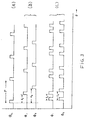
- Fig. 3 illustrates different pulse signal forms useful for discriminating between respective signals ⁇ i .
- Fig. 3(A) shows a clock signal ⁇ CL , i.e., a pulse signal that defines a signal period P.
- Fig. 3(B) shows two signals ⁇ 1 and ⁇ 2 which contain one pulse per signal period P, the time distance t i between the clock signal pulse and the signal pulse being characteristic of those signals ⁇ 1 and ⁇ 2 .
- Fig. 3(C) shows two signals ⁇ 1 and ⁇ 2 which contain two pulses per signal period P, the time distance t i between those two pulses being characteristic of those signals ⁇ 1 and ⁇ 2 .
- control element is preferably of double design, as outlined in Fig. 2 (control elements 100 and 100').
- the corresponding inputs of the two control elements are connected to each other, so that those control elements will, in principle, process identical signals and hence will generate identical output signals.
- the operation of the lift is stopped and an alarm is generated as soon as either of the control elements detects an error situation, and/or as soon as the output signals of the two control elements differ from each other.
- control circuit 200 provided on a printed-circuit board, which control circuit 200 comprises a control element 100 with a plurality of inputs 110 i .
- Operating switches Si are connected with respective inputs 110 i by print tracks 12 i , 30 i .
- a signal source 10 generates a plurality of mutually different signals ⁇ i which are passed to various switches Si, and whose characteristic is priorly known.
- a signal of a switch may end up at an input of the control element that does not correspond with that switch, but the control element can recognize this error situation because the received signal then has the wrong characteristic.
- the control element can then ignore the operating instruction, and/or generate an alarm signal.
- the present invention is not limited to the field of lifts.
- other appliances or processes are conceivable, where a control element must make decisions on the basis of a plurality of switches, and the present invention can be of use there too.
- a microwave oven can be mentioned.
- the switches may also be opto-electrical switches.
- the signals ⁇ i are generated by the control element, in other words, that the control element and the signal source are integrated into a single unit.
Landscapes
- Engineering & Computer Science (AREA)
- Theoretical Computer Science (AREA)
- General Engineering & Computer Science (AREA)
- Quality & Reliability (AREA)
- Physics & Mathematics (AREA)
- General Physics & Mathematics (AREA)
- Computer Hardware Design (AREA)
- Automation & Control Theory (AREA)
- Structure Of Printed Boards (AREA)
- Safety Devices In Control Systems (AREA)
- Indicating And Signalling Devices For Elevators (AREA)
- Input From Keyboards Or The Like (AREA)
- Keying Circuit Devices (AREA)
- Electronic Switches (AREA)
- Transmission And Conversion Of Sensor Element Output (AREA)
Applications Claiming Priority (2)
| Application Number | Priority Date | Filing Date | Title |
|---|---|---|---|
| NL1007129A NL1007129C2 (nl) | 1997-09-26 | 1997-09-26 | Besturingsschakeling. |
| NL1007129 | 1997-09-26 |
Publications (1)
| Publication Number | Publication Date |
|---|---|
| EP0906886A1 true EP0906886A1 (fr) | 1999-04-07 |
Family
ID=19765742
Family Applications (1)
| Application Number | Title | Priority Date | Filing Date |
|---|---|---|---|
| EP19980203241 Withdrawn EP0906886A1 (fr) | 1997-09-26 | 1998-09-28 | Circuit de commande |
Country Status (6)
| Country | Link |
|---|---|
| US (1) | US6075296A (fr) |
| EP (1) | EP0906886A1 (fr) |
| JP (1) | JP2000031800A (fr) |
| KR (1) | KR19990030138A (fr) |
| NL (1) | NL1007129C2 (fr) |
| NO (1) | NO984485L (fr) |
Families Citing this family (6)
| Publication number | Priority date | Publication date | Assignee | Title |
|---|---|---|---|---|
| DE10054588A1 (de) * | 2000-11-03 | 2002-05-08 | Siemens Ag | Für ein Fraftfahrzeug bestimmtes elektronisches Gerät |
| JP5248269B2 (ja) * | 2008-10-31 | 2013-07-31 | 株式会社東芝 | 遮断器の開閉制御装置、及び遮断器の開閉制御システム |
| KR101119698B1 (ko) * | 2010-12-24 | 2012-10-04 | 주식회사 대륙 | 전기 자동차용 아크리스 릴레이, 이의 제어 방법 및 이를 구현하기 위한 프로그램이 기록된 기록매체 |
| JP5703928B2 (ja) * | 2011-04-20 | 2015-04-22 | カシオ計算機株式会社 | キー装置 |
| WO2013073623A1 (fr) | 2011-11-15 | 2013-05-23 | 富士電機株式会社 | Dispositif semi-conducteur et procédé de fabrication du dispositif semi-conducteur |
| EP3443997A1 (fr) | 2017-08-18 | 2019-02-20 | Roche Diabetes Care GmbH | Dispositif médical et procédé de fonctionnement d'un dispositif médical et la détection d'un court-circuit |
Citations (4)
| Publication number | Priority date | Publication date | Assignee | Title |
|---|---|---|---|---|
| US4002973A (en) * | 1975-12-23 | 1977-01-11 | Armor Elevator Company | Elevator testing system |
| JPS5817457A (ja) * | 1981-07-24 | 1983-02-01 | Fuji Xerox Co Ltd | 入力回路の自己診断装置 |
| JPS60168060A (ja) * | 1984-02-10 | 1985-08-31 | Nec Corp | ボ−ドテスタ |
| JPH0873149A (ja) * | 1994-09-02 | 1996-03-19 | Hitachi Building Syst Eng & Service Co Ltd | エレベータ制御盤のプリント板試験装置 |
Family Cites Families (1)
| Publication number | Priority date | Publication date | Assignee | Title |
|---|---|---|---|---|
| JPS58208911A (ja) * | 1982-05-27 | 1983-12-05 | Matsushita Electric Ind Co Ltd | 磁気記録再生装置 |
-
1997
- 1997-09-26 NL NL1007129A patent/NL1007129C2/nl active Search and Examination
-
1998
- 1998-09-23 US US09/158,849 patent/US6075296A/en not_active Expired - Fee Related
- 1998-09-25 KR KR1019980039885A patent/KR19990030138A/ko not_active Application Discontinuation
- 1998-09-25 NO NO984485A patent/NO984485L/no not_active Application Discontinuation
- 1998-09-25 JP JP30774298A patent/JP2000031800A/ja active Pending
- 1998-09-28 EP EP19980203241 patent/EP0906886A1/fr not_active Withdrawn
Patent Citations (4)
| Publication number | Priority date | Publication date | Assignee | Title |
|---|---|---|---|---|
| US4002973A (en) * | 1975-12-23 | 1977-01-11 | Armor Elevator Company | Elevator testing system |
| JPS5817457A (ja) * | 1981-07-24 | 1983-02-01 | Fuji Xerox Co Ltd | 入力回路の自己診断装置 |
| JPS60168060A (ja) * | 1984-02-10 | 1985-08-31 | Nec Corp | ボ−ドテスタ |
| JPH0873149A (ja) * | 1994-09-02 | 1996-03-19 | Hitachi Building Syst Eng & Service Co Ltd | エレベータ制御盤のプリント板試験装置 |
Non-Patent Citations (3)
| Title |
|---|
| PATENT ABSTRACTS OF JAPAN vol. 10, no. 12 (P - 421)<2069> 17 January 1986 (1986-01-17) * |
| PATENT ABSTRACTS OF JAPAN vol. 7, no. 90 (P - 191) 14 April 1983 (1983-04-14) * |
| PATENT ABSTRACTS OF JAPAN vol. 96, no. 7 31 July 1996 (1996-07-31) * |
Also Published As
| Publication number | Publication date |
|---|---|
| JP2000031800A (ja) | 2000-01-28 |
| US6075296A (en) | 2000-06-13 |
| NO984485L (no) | 1999-03-29 |
| KR19990030138A (ko) | 1999-04-26 |
| NL1007129C2 (nl) | 1999-05-04 |
| NL1007129A1 (nl) | 1999-03-29 |
| NO984485D0 (no) | 1998-09-25 |
Similar Documents
| Publication | Publication Date | Title |
|---|---|---|
| JP3187990B2 (ja) | 多重負荷を切り換える電子制御装置 | |
| US20020180278A1 (en) | Circuit arrangement and device for safely disconnecting an element in an installation, in particular a machine installation | |
| US6075296A (en) | Control circuit | |
| US6201363B1 (en) | Power window apparatus | |
| EP0920134B1 (fr) | Circuit interface | |
| US5374920A (en) | Directional and warning blink apparatus for a vehicle, particularly a motor vehicle | |
| CN114026445A (zh) | 用于监控电气安全互锁的装置和方法 | |
| US9679726B2 (en) | Anti-interference switch signal transmission circuit | |
| US7304406B2 (en) | Control device for safety-critical components and corresponding method | |
| US11119156B2 (en) | Monitoring arrangement for monitoring a safety sensor and method for monitoring a safety sensor | |
| JPH11283456A (ja) | スイッチおよびそれを備えた情報検出装置、ならびにコネクタ接続状態検出装置 | |
| JPH07282702A (ja) | 時間プログラムに従ってスイッチング装置を操作する制御装置 | |
| JP4317590B2 (ja) | 中断のない発生器によるテストのための回路配置および方法 | |
| KR20010052224A (ko) | 버스 시스템에서 디지털 전압 신호를 발생시키기 위한시그널링 출력단 | |
| US11101090B2 (en) | Digital signal output device that outputs a digital signal in accordance with operation switch | |
| US7112899B2 (en) | Device for controlling an electric load, and a control device | |
| KR19990030176A (ko) | 안전스위치 | |
| US20030193766A1 (en) | Switching Device For Signaling A Binary Information Item | |
| US20230266495A1 (en) | Sensor | |
| KR101407912B1 (ko) | 토크센서 고장 검출 장치 및 토크센서 | |
| JP2774310B2 (ja) | 論理演算器及び同論理演算器を用いた制御装置 | |
| WO2001095499A1 (fr) | Dispositif et procede permettant de reduire l'electromigration | |
| SU1170424A1 (ru) | Устройство блокировки привода | |
| JPS62245901A (ja) | 位置検出装置 | |
| JPH03256499A (ja) | 選択制御回路 |
Legal Events
| Date | Code | Title | Description |
|---|---|---|---|
| PUAI | Public reference made under article 153(3) epc to a published international application that has entered the european phase |
Free format text: ORIGINAL CODE: 0009012 |
|
| AK | Designated contracting states |
Kind code of ref document: A1 Designated state(s): AT BE CH CY DE DK ES FI FR GB GR IE IT LI LU MC NL PT SE |
|
| AX | Request for extension of the european patent |
Free format text: AL;LT;LV;MK;RO;SI |
|
| 17P | Request for examination filed |
Effective date: 19990929 |
|
| AKX | Designation fees paid |
Free format text: AT BE CH CY DE DK ES FI FR GB GR IE IT LI LU MC NL PT SE |
|
| AXX | Extension fees paid |
Free format text: AL PAYMENT 19990929;LT PAYMENT 19990929;LV PAYMENT 19990929;MK PAYMENT 19990929;RO PAYMENT 19990929;SI PAYMENT 19990929 |
|
| STAA | Information on the status of an ep patent application or granted ep patent |
Free format text: STATUS: THE APPLICATION IS DEEMED TO BE WITHDRAWN |
|
| 18D | Application deemed to be withdrawn |
Effective date: 20030401 |