EP0905794A2 - Cellule solaire et procédé de fabrication - Google Patents
Cellule solaire et procédé de fabrication Download PDFInfo
- Publication number
- EP0905794A2 EP0905794A2 EP98117981A EP98117981A EP0905794A2 EP 0905794 A2 EP0905794 A2 EP 0905794A2 EP 98117981 A EP98117981 A EP 98117981A EP 98117981 A EP98117981 A EP 98117981A EP 0905794 A2 EP0905794 A2 EP 0905794A2
- Authority
- EP
- European Patent Office
- Prior art keywords
- flank
- electrically conductive
- solar cell
- area
- region
- Prior art date
- Legal status (The legal status is an assumption and is not a legal conclusion. Google has not performed a legal analysis and makes no representation as to the accuracy of the status listed.)
- Granted
Links
- 238000004519 manufacturing process Methods 0.000 title claims abstract description 16
- 239000004065 semiconductor Substances 0.000 claims abstract description 47
- 239000004020 conductor Substances 0.000 claims abstract description 25
- 239000000463 material Substances 0.000 claims abstract description 15
- 239000002800 charge carrier Substances 0.000 claims abstract description 9
- 230000005855 radiation Effects 0.000 claims abstract description 9
- 230000005684 electric field Effects 0.000 claims abstract description 5
- 238000000034 method Methods 0.000 claims description 28
- 239000000758 substrate Substances 0.000 claims description 20
- 238000005530 etching Methods 0.000 claims description 7
- 238000000151 deposition Methods 0.000 claims description 3
- 238000002161 passivation Methods 0.000 claims description 3
- 238000005240 physical vapour deposition Methods 0.000 claims description 3
- 239000012212 insulator Substances 0.000 claims 2
- 210000004027 cell Anatomy 0.000 description 61
- 229910052751 metal Inorganic materials 0.000 description 22
- 239000002184 metal Substances 0.000 description 22
- 238000009792 diffusion process Methods 0.000 description 15
- 238000001704 evaporation Methods 0.000 description 13
- 230000008020 evaporation Effects 0.000 description 13
- 238000007740 vapor deposition Methods 0.000 description 11
- 238000013461 design Methods 0.000 description 9
- 239000010410 layer Substances 0.000 description 9
- 230000008901 benefit Effects 0.000 description 7
- 230000008569 process Effects 0.000 description 7
- 238000001465 metallisation Methods 0.000 description 6
- 230000015572 biosynthetic process Effects 0.000 description 5
- XUIMIQQOPSSXEZ-UHFFFAOYSA-N Silicon Chemical compound [Si] XUIMIQQOPSSXEZ-UHFFFAOYSA-N 0.000 description 4
- 229910052782 aluminium Inorganic materials 0.000 description 4
- XAGFODPZIPBFFR-UHFFFAOYSA-N aluminium Chemical compound [Al] XAGFODPZIPBFFR-UHFFFAOYSA-N 0.000 description 4
- 230000004888 barrier function Effects 0.000 description 4
- 238000007650 screen-printing Methods 0.000 description 4
- 229910052710 silicon Inorganic materials 0.000 description 4
- 239000010703 silicon Substances 0.000 description 4
- 238000012549 training Methods 0.000 description 4
- 238000007738 vacuum evaporation Methods 0.000 description 4
- 229910052581 Si3N4 Inorganic materials 0.000 description 3
- 238000005266 casting Methods 0.000 description 3
- 239000003795 chemical substances by application Substances 0.000 description 3
- 230000000873 masking effect Effects 0.000 description 3
- 230000006798 recombination Effects 0.000 description 3
- 238000005215 recombination Methods 0.000 description 3
- HQVNEWCFYHHQES-UHFFFAOYSA-N silicon nitride Chemical compound N12[Si]34N5[Si]62N3[Si]51N64 HQVNEWCFYHHQES-UHFFFAOYSA-N 0.000 description 3
- KRHYYFGTRYWZRS-UHFFFAOYSA-N Fluorane Chemical compound F KRHYYFGTRYWZRS-UHFFFAOYSA-N 0.000 description 2
- VEXZGXHMUGYJMC-UHFFFAOYSA-N Hydrochloric acid Chemical compound Cl VEXZGXHMUGYJMC-UHFFFAOYSA-N 0.000 description 2
- PXHVJJICTQNCMI-UHFFFAOYSA-N Nickel Chemical compound [Ni] PXHVJJICTQNCMI-UHFFFAOYSA-N 0.000 description 2
- 238000004140 cleaning Methods 0.000 description 2
- 230000008021 deposition Effects 0.000 description 2
- 229910003460 diamond Inorganic materials 0.000 description 2
- 239000010432 diamond Substances 0.000 description 2
- 239000002019 doping agent Substances 0.000 description 2
- 238000009713 electroplating Methods 0.000 description 2
- 238000005516 engineering process Methods 0.000 description 2
- 238000009776 industrial production Methods 0.000 description 2
- 238000000623 plasma-assisted chemical vapour deposition Methods 0.000 description 2
- 230000009467 reduction Effects 0.000 description 2
- 230000005082 stem growth Effects 0.000 description 2
- 239000000126 substance Substances 0.000 description 2
- NLXLAEXVIDQMFP-UHFFFAOYSA-N Ammonium chloride Substances [NH4+].[Cl-] NLXLAEXVIDQMFP-UHFFFAOYSA-N 0.000 description 1
- VHUUQVKOLVNVRT-UHFFFAOYSA-N Ammonium hydroxide Chemical compound [NH4+].[OH-] VHUUQVKOLVNVRT-UHFFFAOYSA-N 0.000 description 1
- RYGMFSIKBFXOCR-UHFFFAOYSA-N Copper Chemical compound [Cu] RYGMFSIKBFXOCR-UHFFFAOYSA-N 0.000 description 1
- OAICVXFJPJFONN-UHFFFAOYSA-N Phosphorus Chemical compound [P] OAICVXFJPJFONN-UHFFFAOYSA-N 0.000 description 1
- BQCADISMDOOEFD-UHFFFAOYSA-N Silver Chemical compound [Ag] BQCADISMDOOEFD-UHFFFAOYSA-N 0.000 description 1
- 238000005299 abrasion Methods 0.000 description 1
- 239000004411 aluminium Substances 0.000 description 1
- 235000011114 ammonium hydroxide Nutrition 0.000 description 1
- 239000006117 anti-reflective coating Substances 0.000 description 1
- 230000003667 anti-reflective effect Effects 0.000 description 1
- 238000013459 approach Methods 0.000 description 1
- 229910001417 caesium ion Inorganic materials 0.000 description 1
- 239000000969 carrier Substances 0.000 description 1
- 150000001875 compounds Chemical class 0.000 description 1
- 239000000356 contaminant Substances 0.000 description 1
- 229910052802 copper Inorganic materials 0.000 description 1
- 239000010949 copper Substances 0.000 description 1
- 238000005260 corrosion Methods 0.000 description 1
- 230000007797 corrosion Effects 0.000 description 1
- 230000008878 coupling Effects 0.000 description 1
- 238000010168 coupling process Methods 0.000 description 1
- 238000005859 coupling reaction Methods 0.000 description 1
- 239000013078 crystal Substances 0.000 description 1
- 229910021419 crystalline silicon Inorganic materials 0.000 description 1
- 230000003247 decreasing effect Effects 0.000 description 1
- 230000001627 detrimental effect Effects 0.000 description 1
- 230000000694 effects Effects 0.000 description 1
- 238000007772 electroless plating Methods 0.000 description 1
- 238000000227 grinding Methods 0.000 description 1
- 230000006872 improvement Effects 0.000 description 1
- 239000012535 impurity Substances 0.000 description 1
- 239000007788 liquid Substances 0.000 description 1
- 150000002739 metals Chemical class 0.000 description 1
- 229910052759 nickel Inorganic materials 0.000 description 1
- 230000003287 optical effect Effects 0.000 description 1
- 229910052698 phosphorus Inorganic materials 0.000 description 1
- 239000011574 phosphorus Substances 0.000 description 1
- 230000008092 positive effect Effects 0.000 description 1
- 238000012545 processing Methods 0.000 description 1
- 238000003672 processing method Methods 0.000 description 1
- 230000035945 sensitivity Effects 0.000 description 1
- 229910052709 silver Inorganic materials 0.000 description 1
- 239000004332 silver Substances 0.000 description 1
- 238000005245 sintering Methods 0.000 description 1
- 239000007787 solid Substances 0.000 description 1
- 239000002904 solvent Substances 0.000 description 1
- 238000009987 spinning Methods 0.000 description 1
- 239000002344 surface layer Substances 0.000 description 1
- 239000010409 thin film Substances 0.000 description 1
- 230000007704 transition Effects 0.000 description 1
- 239000002699 waste material Substances 0.000 description 1
Images


Classifications
-
- H—ELECTRICITY
- H01—ELECTRIC ELEMENTS
- H01L—SEMICONDUCTOR DEVICES NOT COVERED BY CLASS H10
- H01L31/00—Semiconductor devices sensitive to infrared radiation, light, electromagnetic radiation of shorter wavelength or corpuscular radiation and specially adapted either for the conversion of the energy of such radiation into electrical energy or for the control of electrical energy by such radiation; Processes or apparatus specially adapted for the manufacture or treatment thereof or of parts thereof; Details thereof
- H01L31/02—Details
- H01L31/0224—Electrodes
- H01L31/022408—Electrodes for devices characterised by at least one potential jump barrier or surface barrier
- H01L31/022425—Electrodes for devices characterised by at least one potential jump barrier or surface barrier for solar cells
-
- H—ELECTRICITY
- H01—ELECTRIC ELEMENTS
- H01L—SEMICONDUCTOR DEVICES NOT COVERED BY CLASS H10
- H01L31/00—Semiconductor devices sensitive to infrared radiation, light, electromagnetic radiation of shorter wavelength or corpuscular radiation and specially adapted either for the conversion of the energy of such radiation into electrical energy or for the control of electrical energy by such radiation; Processes or apparatus specially adapted for the manufacture or treatment thereof or of parts thereof; Details thereof
- H01L31/02—Details
- H01L31/0236—Special surface textures
- H01L31/02363—Special surface textures of the semiconductor body itself, e.g. textured active layers
-
- H—ELECTRICITY
- H01—ELECTRIC ELEMENTS
- H01L—SEMICONDUCTOR DEVICES NOT COVERED BY CLASS H10
- H01L31/00—Semiconductor devices sensitive to infrared radiation, light, electromagnetic radiation of shorter wavelength or corpuscular radiation and specially adapted either for the conversion of the energy of such radiation into electrical energy or for the control of electrical energy by such radiation; Processes or apparatus specially adapted for the manufacture or treatment thereof or of parts thereof; Details thereof
- H01L31/04—Semiconductor devices sensitive to infrared radiation, light, electromagnetic radiation of shorter wavelength or corpuscular radiation and specially adapted either for the conversion of the energy of such radiation into electrical energy or for the control of electrical energy by such radiation; Processes or apparatus specially adapted for the manufacture or treatment thereof or of parts thereof; Details thereof adapted as photovoltaic [PV] conversion devices
- H01L31/06—Semiconductor devices sensitive to infrared radiation, light, electromagnetic radiation of shorter wavelength or corpuscular radiation and specially adapted either for the conversion of the energy of such radiation into electrical energy or for the control of electrical energy by such radiation; Processes or apparatus specially adapted for the manufacture or treatment thereof or of parts thereof; Details thereof adapted as photovoltaic [PV] conversion devices characterised by at least one potential-jump barrier or surface barrier
- H01L31/062—Semiconductor devices sensitive to infrared radiation, light, electromagnetic radiation of shorter wavelength or corpuscular radiation and specially adapted either for the conversion of the energy of such radiation into electrical energy or for the control of electrical energy by such radiation; Processes or apparatus specially adapted for the manufacture or treatment thereof or of parts thereof; Details thereof adapted as photovoltaic [PV] conversion devices characterised by at least one potential-jump barrier or surface barrier the potential barriers being only of the metal-insulator-semiconductor type
-
- Y—GENERAL TAGGING OF NEW TECHNOLOGICAL DEVELOPMENTS; GENERAL TAGGING OF CROSS-SECTIONAL TECHNOLOGIES SPANNING OVER SEVERAL SECTIONS OF THE IPC; TECHNICAL SUBJECTS COVERED BY FORMER USPC CROSS-REFERENCE ART COLLECTIONS [XRACs] AND DIGESTS
- Y02—TECHNOLOGIES OR APPLICATIONS FOR MITIGATION OR ADAPTATION AGAINST CLIMATE CHANGE
- Y02E—REDUCTION OF GREENHOUSE GAS [GHG] EMISSIONS, RELATED TO ENERGY GENERATION, TRANSMISSION OR DISTRIBUTION
- Y02E10/00—Energy generation through renewable energy sources
- Y02E10/50—Photovoltaic [PV] energy
Definitions
- the invention relates to a solar cell comprising a semi-material in which can be generated by incident radiation energy, the charge carriers electrical field separable and then via first and second electrically conductive contacts are derivable, with groove-shaped depressions on at least one semiconductor surface each with at least one flank-like area, of which at least a flank-like area indirectly or directly electrically conductive material for Formation of a first electrically conductive contact is applied.
- the Invention relating to a method for producing a solar cell comprising a semiconductor material, in which charge carriers can be generated by incident radiation energy separable by an electric field and then via first and second electrically conductive Contacts can be derived, with groove-shaped depressions on a semiconductor surface first flank-like areas are formed, on which indirectly or directly electrically conductive material for forming one of the electrically conductive contacts is applied.
- BCSC Battery Contact solar cell
- This method of oblique evaporation makes the usual Disadvantages of conventional vertical vapor deposition avoided with a shadow mask because the design of the self-shading elevations on the one hand on the Use of a shadow mask to define the contact grid can be omitted and on the other hand the system throughput compared to vertical evaporation can be increased significantly because the solar cells at a very flat angle The direction of evaporation can be arranged very closely (Hezel Proc. 13th European Photovoltaik Solar Energy Conference, Nice, 1995, p. 115).
- the evaporation material becomes a lot better exploited than in vertical evaporation, in which most of the Metals envious of the masks and only then labor-intensive etched from them must become.
- the method presented here allows the finger width to be varied essentially by varying the vapor deposition angle, since the width of the trench is mostly determined by the used tools (e.g. diamond-tipped saw blade, wire with lapping agent) is.
- the spacing of the individual contact fingers in these structures is immediately determined specified the tool width.
- Cells of this type are currently achieving efficiencies of 18.6% (Verbeek et al., Proc. 25th IEEE Photovoltaic Specialists Conference, Washington D.C., 1996, p. 521). Due to the pressure in the evaporation chamber, the expansion of the Vapor deposition source and the scattering of the material at the shadow casting edges Divergence of the vapor deposition jet is a sharp shadow cast of the elevations only up to a distance of approx.
- a solar cell with a V-shaped surface is formed Trenches described.
- the solar cell is aligned with the incident radiation.
- the distance of the V-shaped Trenches are defined by the substrate orientation and thickness within very narrow limits, the maximum distance being 2.7 times the depth of the grave.
- the present invention is based on the problem of a solar cell and a method to produce such a of the type described above so that by means of simple technology and if necessary using large-scale and in particular Very simple and inexpensive processing methods Solar cells can be produced very efficiently are.
- a high variability in terms of the design of the electrical Charge-conducting electrically conductive contacts may be possible.
- the problem is solved by a solar cell of the type mentioned at the beginning solved in that the flank-like region perpendicular or almost perpendicular to the Semiconductor surface spanned level and that to form the one electrically conductive contact, the electrically conductive material exclusively on the flank-like area is applied. Further training results from the subclaims.
- the problem essentially becomes a method of the type mentioned at the beginning solved in that the flank-like areas are formed such that they perpendicular or almost perpendicular to the plane spanned by the semiconductor surface run, and that the electrically conductive material to form the one electrically conductive contacts without masking and selectively from the areas of the semiconductor surface is removed, which run outside the flank-like area.
- Training result from the subclaims structuring the method.
- the material forming the electrically conductive contacts is preferably without Use a separate mask on the flank-like areas with the method of Vacuum evaporation applied at a flat angle to the substrate plane.
- Another essential feature of the inventive concept is that of Oblique evaporation required surface structure so that on the one hand Shading by the metal fingers with a sufficiently large conductor cross-section as little as possible, on the other hand the material removal required for the production of the structure is minimized.
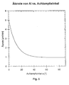
- a basic idea of the present invention is the special stem growth to advantageously use obliquely vapor-deposited metal layers according to the invention. Doing so due to the increasing stem growth with a flatter evaporation angle the separated Layer increasingly porous. The increasing porosity of the layers results, as in FIG. 5 shown a drastic increase in the etching rate under otherwise identical external conditions.
- the exploitation of this effect enables the abovementioned according to the invention trained to use surface structures particularly advantageous, because the on the not deposited metal-like areas is very easy to etch away. Therefore, the Thickness of the actual metal contact can not be designed to be larger by the to compensate for the subsequent loss of thickness.
- the widths not only by the Deposition angle ⁇ or the tool width a, but completely independent of these sizes by the saw depth or flank width b, provided that the tangent of the vapor deposition angle ⁇ is always greater than the ratio of flank width b to distance Shadow edge / flank a (see Fig. 4a-c). This fact enables the manufacturing precise setting of the evaporation angle to handle considerably less critical. It turns out always the same contact width k given by the edge width b.
- a very important feature of the inventive concept is that it can be used as generally as possible
- the technology also allow you to realize finger distances of any size, which for certain Solar cell types is of decisive advantage, because the number of fingers is reduced one reduces shading and thus the short-circuit current of the cell is increased.
- the metal-semiconductor contact area can also be reduced, which in turn the positive effect of an increase in open circuit voltage due to decreased Recombination on the metal contacts.
- the requirements for the tool width and wear are far less, since the BCSC is not as narrow and deep as possible Trenches (with a preferred ratio, width: depth 1: 2-1: 7) are required, but relative wide and flat (preferably width: depth 1: 1-10: 1).
- the shading by the metal contacts is not by the technically feasible trench width is limited downwards, but is due to the Evaporation thickness freely selectable. This is particularly advantageous for low-cost solar cells Finger distance such as B. the type of MIS solar line.
- both parameters can be independent can be optimally designed from each other.
- the surface structures used were used for the structure used for making contacts also the improvement of the light trapping. Because that for optimal light trapping necessary structures in their dimensions in principle by more than an order of magnitude below which the contact distances lie, the two work together in one Structures very detrimental to efficiency.
- This disadvantage can be caused by the Formation of the surface structure according to the invention for producing the electrically Conductive contacts can be eliminated because these structures are particularly simple and in front everything also largely independent of the design of the invention Arrange structures to arrange any substructures that improve light trapping.
- Another inventive concept is preferably in the lower lying area one or more recesses between two electrically conductive contacts to train those who, because of their depth and the depth that extends far into the semiconductor volume pn junction the collection of minority charge carriers in the volume of the semiconductor improve.
- the depressions can be of any geometrical design. By suitable shape (see Fig. 3b), however, the light trapping can also be increased.
- These recesses are preferably made by suitable design of the tool produced simultaneously with the contact recesses.
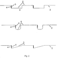
- Fig. 1 shows a schematic representation of a section of a solar cell (1) with at least a semiconductor surface (2) on which edges (3) are formed, which are flank-like Connect areas (4) and electrically conductive contacts (5) directly or indirectly at least some of the flank-like areas are applied.
- the edges and flank-like areas can be easily moved with the help of moving mechanical Structuring elements (e.g. diamond tools, wires with lapping agent) or through Train the use of laser pens.
- the metallization can be done by the method of Vacuum evaporation is done at a small angle to the substrate surface.
- the procedure is as follows: After training the parallel extending edges (3) and their flank-like areas (4) z. B. by means of a diamond-coated grinding wheel is etched off the surface of the solar cell thin surface layer damaged by sawing removed, since this layer with their Dislocations and impurities an increased surface recombination and thus a would result in lower efficiency. This is usually followed by a wet chemical one Cleaning to remove all organic and metallic contaminants from the Remove solar cell surface. The next step is the back of the solar cell with a diffusion barrier from e.g. PECVD silicon nitride provided only on the Front side by diffusion of suitable foreign atoms (e.g. phosphorus with p-doped Substrate) to produce a pn junction.
- a diffusion barrier from e.g. PECVD silicon nitride provided only on the Front side by diffusion of suitable foreign atoms (e.g. phosphorus with p-doped Substrate) to produce a pn junction.
- the diffusion barrier of the back removed by etching in hydrofluoric acid.
- the metallic Back contact applied by vapor deposition or screen printing and sintered.
- the Formation of the front contacts This happens e.g. by physical vapor deposition a metal layer in a vacuum at a flat angle to the substrate surface as well
- the individual conductor tracks are made by applying them an electrically conductive cross-connection (busbar) and the solar cell with an anti-reflective coating e.g. made of PECVD silicon nitride.
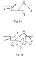
- flank-like areas can vary depending on used tool e.g. be box-shaped, trough-shaped or triangular (see Fig. 2). It is only important according to the invention that a parallel or almost parallel to Flank-like region (4) of sufficient width that is normal to the substrate becomes. Depending on the distance between the fingers, this width is usually between 5 and 50 ⁇ m. Structures that minimize silicon abrasion are advantageous here Training of flank-like areas require structuring costs in the first place Approximation is proportional to the silicon volume to be removed.
- the one shown in Fig. 3b i.a. to improve the collection of minority carriers in the Volume of the semiconductor serving structure (9) has a sawtooth shape, the left Flank additionally reflects the incident light into the semiconductor substrate (2).
- the Laying the collecting pn junction in the semiconductor can vary from approx. 10 ⁇ m to approx. Extend 150 ⁇ m.
- This double function of the structure in terms of optical and electrical situation is especially for chemically not texturable semiconductor materials short diffusion length is an advantage, e.g. multicrystalline or band-drawn material.
- Other forms of deepening to increase the probability of collecting Minority charge carriers are conceivable.
- the pn junction on the front of the solar cell can be generated instead of by diffusion from the gas phase also by spinning on a liquid containing dopant (spin-on dopant). It is also possible to dispense with the application of a diffusion barrier on the rear, if the introduced foreign atoms on the back in a subsequent process step can be compensated by a corresponding second concern of foreign atoms, e.g. by Creation of an aluminum back surface field. Generation of the pn junction (11) but can also by applying solid charges (Cs ions and silicon nitride) and one resulting inversion of the semiconductor surface.
- the contact width k is determined by the vapor deposition angle ⁇ and the distance a of the shadow-casting edge from the flank-like region to be steamed.
- tan ⁇ ⁇ b / a and k a * tan ⁇ , where b indicates the width of the flank-like area.
- the contact width k is determined exclusively by the width b of the flank-like area.
- Another advantageous embodiment of the invention includes the Semiconductor surface (2) before application of the contacts with a passivation layer (7) provided to then open them in narrow contact areas and then with wider ones To provide metal contacts (5), both on the open semiconductor surface and run at least partially on the passivation layer (see Fig. 1 b).
- This allows the a high charge carrier recombination connected metal-semiconductor contact area can be drastically reduced.
- This has an advantageous increase in open circuit voltage and hence the efficiency.
- the electrically conductive metal contact according to the invention not on plateau-like areas but exclusively on the flank-like areas (4) which are parallel or almost parallel to Substrate normals run. This results in a significantly reduced shadowing from the opaque metal fingers and thus an efficiency advantage.
- the inventive method for producing the Rear contacts of solar cells are used. This becomes procedural proceeded in exactly the same way as for the production of the front contacts.
- the metal contacts on the back run perpendicular to the front on possible To minimize series resistance losses.
- the proposal defining the invention the Self-aligning conductor tracks parallel or almost parallel to the substrate normal Applying flank-like areas is also for the solar cell back contact advantageous for several reasons.
- this method enables simple Production of double-sided light-sensitive solar cells, so-called bifacial cells, since not as with conventional solar cells, the entire back is covered with metal. To the others also get all the advantages described for the front to advantage.
- the height of the flank-like region 4 is identified by "b", the perpendicular or almost perpendicular to the spanned by the solar cell surface Level runs.
- the corresponding to a flank-like area 4 from the substrate surface starting next and running in the plane of the substrate surface plateau-like section 20 has a width h. Goes from the plateau-like area 20 the surface 24 extending to the bottom edge 22 of the flank-like region 4.
- the edge SK formed by the transition of surfaces 20, 22 is a so-called shadow-casting edge, which, depending on the evaporation angle ⁇ , specifies the height of the electrically conductive material on the flank-like area 4 to form the electrically conductive contact 5 is deposited. The corresponding height is marked with k.
- the width is of the plateau-like region 20 "h” and that of the surface 24 "a” which runs obliquely thereto wherein the width a of the surface 24 is greater than the height b of the flank-like region 4, in particular a> 3 b.
- the distance between successive flank-like areas 4 on which electrically conductive contacts 5 is A, in particular 100 microns ⁇ A ⁇ 2000 ⁇ m should be.
- the height b of the flank-like areas themselves is preferably 5 ⁇ m ⁇ b ⁇ 200 ⁇ m.
- each depression is delimited by two flank-like areas 4, 26, of which one is provided with the electrically conductive material and each perpendicular to that of of the solar cell surface 30 spanned plane.
- the flank-like ones are corresponding with the electrically conductive material provided areas 4 of the other embodiments also perpendicular to that spanned by the semiconductor material surface Level aligned.
- the first and second having the same or substantially the same height Flanks 4, 26 are connected via a bottom surface 28 of the depression.
- the course of the flanks 4, 26 and the bottom surface 28 results in the desired box-shaped Geometry of the depression.
Applications Claiming Priority (3)
| Application Number | Priority Date | Filing Date | Title |
|---|---|---|---|
| DE19741832A DE19741832A1 (de) | 1997-09-23 | 1997-09-23 | Verfahren zur Herstellung einer Solarzelle und Solarzelle |
| DE19741832 | 1997-09-23 | ||
| US09/282,199 US6172297B1 (en) | 1997-09-23 | 1999-03-31 | Solar cell and method for fabrication of a solar cell |
Publications (3)
| Publication Number | Publication Date |
|---|---|
| EP0905794A2 true EP0905794A2 (fr) | 1999-03-31 |
| EP0905794A3 EP0905794A3 (fr) | 1999-12-29 |
| EP0905794B1 EP0905794B1 (fr) | 2004-12-29 |
Family
ID=26040210
Family Applications (1)
| Application Number | Title | Priority Date | Filing Date |
|---|---|---|---|
| EP98117981A Expired - Lifetime EP0905794B1 (fr) | 1997-09-23 | 1998-09-23 | Cellule solaire et procédé de fabrication |
Country Status (4)
| Country | Link |
|---|---|
| US (1) | US6172297B1 (fr) |
| EP (1) | EP0905794B1 (fr) |
| DE (2) | DE19741832A1 (fr) |
| ES (1) | ES2236854T3 (fr) |
Cited By (4)
| Publication number | Priority date | Publication date | Assignee | Title |
|---|---|---|---|---|
| US6963024B2 (en) | 2001-02-01 | 2005-11-08 | Shin-Etsu Handotai Co., Ltd. | Solar cell module and its installing module |
| US7355114B2 (en) | 2001-03-19 | 2008-04-08 | Shin-Etsu Handotai Co., Ltd. | Solar cell and its manufacturing method |
| US8013239B2 (en) | 2002-08-29 | 2011-09-06 | Day4 Energy Inc. | Electrode for photovoltaic cells, photovoltaic cell and photovoltaic module |
| US8293568B2 (en) | 2008-07-28 | 2012-10-23 | Day4 Energy Inc. | Crystalline silicon PV cell with selective emitter produced with low temperature precision etch back and passivation process |
Families Citing this family (70)
| Publication number | Priority date | Publication date | Assignee | Title |
|---|---|---|---|---|
| US8664030B2 (en) | 1999-03-30 | 2014-03-04 | Daniel Luch | Collector grid and interconnect structures for photovoltaic arrays and modules |
| AUPR174800A0 (en) * | 2000-11-29 | 2000-12-21 | Australian National University, The | Semiconductor processing |
| WO2003047004A1 (fr) * | 2001-11-29 | 2003-06-05 | Origin Energy Solar Pty Ltd | Procede de texturation de semiconducteurs |
| KR100831291B1 (ko) * | 2001-01-31 | 2008-05-22 | 신에쯔 한도타이 가부시키가이샤 | 태양전지 및 태양전지의 제조방법 |
| JP2002305311A (ja) * | 2001-01-31 | 2002-10-18 | Shin Etsu Handotai Co Ltd | 太陽電池の製造方法および太陽電池 |
| US6780665B2 (en) * | 2001-08-28 | 2004-08-24 | Romain Louis Billiet | Photovoltaic cells from silicon kerf |
| DE10142481A1 (de) * | 2001-08-31 | 2003-03-27 | Rudolf Hezel | Solarzelle sowie Verfahren zur Herstellung einer solchen |
| US20050126619A1 (en) * | 2002-02-28 | 2005-06-16 | Shin-Etsu Handotai Co., Ltd | Solar cell module and manufacturing method thereof |
| US20050189013A1 (en) * | 2003-12-23 | 2005-09-01 | Oliver Hartley | Process for manufacturing photovoltaic cells |
| WO2006107154A1 (fr) * | 2005-03-16 | 2006-10-12 | Korea Advanced Institute Of Science And Technology | Cellules solaires à film mince intégrées et procédé de fabrication idoine et procédé de traitement d’électrode transparente pour cellules solaires à film mince intégrées et structure idoine, et substrat transparent ayant une électrode |
| KR100656738B1 (ko) * | 2005-12-14 | 2006-12-14 | 한국과학기술원 | 집적형 박막 태양전지 및 그 제조 방법 |
| KR100725110B1 (ko) * | 2005-12-14 | 2007-06-04 | 한국과학기술원 | 투과형 집적형 박막 태양전지 및 그 제조 방법. |
| US20070144577A1 (en) * | 2005-12-23 | 2007-06-28 | Rubin George L | Solar cell with physically separated distributed electrical contacts |
| US7498508B2 (en) * | 2006-02-24 | 2009-03-03 | Day4 Energy, Inc. | High voltage solar cell and solar cell module |
| US9865758B2 (en) | 2006-04-13 | 2018-01-09 | Daniel Luch | Collector grid and interconnect structures for photovoltaic arrays and modules |
| US8884155B2 (en) | 2006-04-13 | 2014-11-11 | Daniel Luch | Collector grid and interconnect structures for photovoltaic arrays and modules |
| US8729385B2 (en) | 2006-04-13 | 2014-05-20 | Daniel Luch | Collector grid and interconnect structures for photovoltaic arrays and modules |
| US9236512B2 (en) | 2006-04-13 | 2016-01-12 | Daniel Luch | Collector grid and interconnect structures for photovoltaic arrays and modules |
| US9006563B2 (en) | 2006-04-13 | 2015-04-14 | Solannex, Inc. | Collector grid and interconnect structures for photovoltaic arrays and modules |
| US8822810B2 (en) | 2006-04-13 | 2014-09-02 | Daniel Luch | Collector grid and interconnect structures for photovoltaic arrays and modules |
| US8017860B2 (en) | 2006-05-15 | 2011-09-13 | Stion Corporation | Method and structure for thin film photovoltaic materials using bulk semiconductor materials |
| US20080092944A1 (en) * | 2006-10-16 | 2008-04-24 | Leonid Rubin | Semiconductor structure and process for forming ohmic connections to a semiconductor structure |
| US20100147368A1 (en) * | 2007-05-17 | 2010-06-17 | Day4 Energy Inc. | Photovoltaic cell with shallow emitter |
| US20080290368A1 (en) * | 2007-05-21 | 2008-11-27 | Day4 Energy, Inc. | Photovoltaic cell with shallow emitter |
| US20080300918A1 (en) * | 2007-05-29 | 2008-12-04 | Commercenet Consortium, Inc. | System and method for facilitating hospital scheduling and support |
| US8071179B2 (en) | 2007-06-29 | 2011-12-06 | Stion Corporation | Methods for infusing one or more materials into nano-voids if nanoporous or nanostructured materials |
| US8759671B2 (en) * | 2007-09-28 | 2014-06-24 | Stion Corporation | Thin film metal oxide bearing semiconductor material for single junction solar cell devices |
| US8287942B1 (en) | 2007-09-28 | 2012-10-16 | Stion Corporation | Method for manufacture of semiconductor bearing thin film material |
| US7998762B1 (en) | 2007-11-14 | 2011-08-16 | Stion Corporation | Method and system for large scale manufacture of thin film photovoltaic devices using multi-chamber configuration |
| CN101919066A (zh) * | 2007-12-18 | 2010-12-15 | 达伊4能量有限公司 | 具有对光伏链的边缘接入的光伏模块、互连方法、装置和系统 |
| US8642138B2 (en) | 2008-06-11 | 2014-02-04 | Stion Corporation | Processing method for cleaning sulfur entities of contact regions |
| US8003432B2 (en) | 2008-06-25 | 2011-08-23 | Stion Corporation | Consumable adhesive layer for thin film photovoltaic material |
| US9087943B2 (en) * | 2008-06-25 | 2015-07-21 | Stion Corporation | High efficiency photovoltaic cell and manufacturing method free of metal disulfide barrier material |
| US8049097B2 (en) * | 2008-08-11 | 2011-11-01 | General Electric Company | Solar cell including cooling channels and method for fabrication |
| US7855089B2 (en) * | 2008-09-10 | 2010-12-21 | Stion Corporation | Application specific solar cell and method for manufacture using thin film photovoltaic materials |
| US8501521B1 (en) | 2008-09-29 | 2013-08-06 | Stion Corporation | Copper species surface treatment of thin film photovoltaic cell and manufacturing method |
| US8008112B1 (en) | 2008-09-29 | 2011-08-30 | Stion Corporation | Bulk chloride species treatment of thin film photovoltaic cell and manufacturing method |
| US8394662B1 (en) | 2008-09-29 | 2013-03-12 | Stion Corporation | Chloride species surface treatment of thin film photovoltaic cell and manufacturing method |
| US8236597B1 (en) | 2008-09-29 | 2012-08-07 | Stion Corporation | Bulk metal species treatment of thin film photovoltaic cell and manufacturing method |
| US8026122B1 (en) | 2008-09-29 | 2011-09-27 | Stion Corporation | Metal species surface treatment of thin film photovoltaic cell and manufacturing method |
| US8476104B1 (en) | 2008-09-29 | 2013-07-02 | Stion Corporation | Sodium species surface treatment of thin film photovoltaic cell and manufacturing method |
| US8008110B1 (en) | 2008-09-29 | 2011-08-30 | Stion Corporation | Bulk sodium species treatment of thin film photovoltaic cell and manufacturing method |
| US8383450B2 (en) * | 2008-09-30 | 2013-02-26 | Stion Corporation | Large scale chemical bath system and method for cadmium sulfide processing of thin film photovoltaic materials |
| US7863074B2 (en) * | 2008-09-30 | 2011-01-04 | Stion Corporation | Patterning electrode materials free from berm structures for thin film photovoltaic cells |
| US8425739B1 (en) | 2008-09-30 | 2013-04-23 | Stion Corporation | In chamber sodium doping process and system for large scale cigs based thin film photovoltaic materials |
| US7910399B1 (en) * | 2008-09-30 | 2011-03-22 | Stion Corporation | Thermal management and method for large scale processing of CIS and/or CIGS based thin films overlying glass substrates |
| US7947524B2 (en) * | 2008-09-30 | 2011-05-24 | Stion Corporation | Humidity control and method for thin film photovoltaic materials |
| US8741689B2 (en) * | 2008-10-01 | 2014-06-03 | Stion Corporation | Thermal pre-treatment process for soda lime glass substrate for thin film photovoltaic materials |
| US20110018103A1 (en) | 2008-10-02 | 2011-01-27 | Stion Corporation | System and method for transferring substrates in large scale processing of cigs and/or cis devices |
| US8003430B1 (en) | 2008-10-06 | 2011-08-23 | Stion Corporation | Sulfide species treatment of thin film photovoltaic cell and manufacturing method |
| US8435826B1 (en) | 2008-10-06 | 2013-05-07 | Stion Corporation | Bulk sulfide species treatment of thin film photovoltaic cell and manufacturing method |
| US8168463B2 (en) | 2008-10-17 | 2012-05-01 | Stion Corporation | Zinc oxide film method and structure for CIGS cell |
| US8344243B2 (en) * | 2008-11-20 | 2013-01-01 | Stion Corporation | Method and structure for thin film photovoltaic cell using similar material junction |
| KR101028971B1 (ko) * | 2009-05-26 | 2011-04-19 | 한국과학기술원 | 집적형 박막 태양전지 및 그의 제조 방법 |
| US8507786B1 (en) | 2009-06-27 | 2013-08-13 | Stion Corporation | Manufacturing method for patterning CIGS/CIS solar cells |
| US8398772B1 (en) | 2009-08-18 | 2013-03-19 | Stion Corporation | Method and structure for processing thin film PV cells with improved temperature uniformity |
| US8809096B1 (en) | 2009-10-22 | 2014-08-19 | Stion Corporation | Bell jar extraction tool method and apparatus for thin film photovoltaic materials |
| US8324015B2 (en) * | 2009-12-01 | 2012-12-04 | Sunpower Corporation | Solar cell contact formation using laser ablation |
| US8859880B2 (en) | 2010-01-22 | 2014-10-14 | Stion Corporation | Method and structure for tiling industrial thin-film solar devices |
| US8263494B2 (en) | 2010-01-25 | 2012-09-11 | Stion Corporation | Method for improved patterning accuracy for thin film photovoltaic panels |
| US9096930B2 (en) | 2010-03-29 | 2015-08-04 | Stion Corporation | Apparatus for manufacturing thin film photovoltaic devices |
| US8263899B2 (en) | 2010-07-01 | 2012-09-11 | Sunpower Corporation | High throughput solar cell ablation system |
| US8461061B2 (en) | 2010-07-23 | 2013-06-11 | Stion Corporation | Quartz boat method and apparatus for thin film thermal treatment |
| US8628997B2 (en) | 2010-10-01 | 2014-01-14 | Stion Corporation | Method and device for cadmium-free solar cells |
| US8728200B1 (en) | 2011-01-14 | 2014-05-20 | Stion Corporation | Method and system for recycling processing gas for selenization of thin film photovoltaic materials |
| US8998606B2 (en) | 2011-01-14 | 2015-04-07 | Stion Corporation | Apparatus and method utilizing forced convection for uniform thermal treatment of thin film devices |
| US8436445B2 (en) | 2011-08-15 | 2013-05-07 | Stion Corporation | Method of manufacture of sodium doped CIGS/CIGSS absorber layers for high efficiency photovoltaic devices |
| FR2993704A1 (fr) * | 2012-07-23 | 2014-01-24 | Commissariat Energie Atomique | Procede de formation de motifs a la surface d'une plaquette en silicium et plaquette de silicium obtenue grace a un tel procede |
| JP6300712B2 (ja) * | 2014-01-27 | 2018-03-28 | 三菱電機株式会社 | 太陽電池および太陽電池の製造方法 |
| DE102014211227A1 (de) | 2014-06-12 | 2015-12-17 | Fraunhofer-Gesellschaft zur Förderung der angewandten Forschung e.V. | Verfahren zur selektiven Entfernung von Background-Plating auf Solarzellen |
Citations (2)
| Publication number | Priority date | Publication date | Assignee | Title |
|---|---|---|---|---|
| US4379944A (en) * | 1981-02-05 | 1983-04-12 | Varian Associates, Inc. | Grooved solar cell for deployment at set angle |
| EP0561615A2 (fr) * | 1992-03-18 | 1993-09-22 | Philips Electronics Uk Limited | Dispositifs de détection infrarouge et leur fabrication |
Family Cites Families (21)
| Publication number | Priority date | Publication date | Assignee | Title |
|---|---|---|---|---|
| DE2754652A1 (de) * | 1977-12-08 | 1979-06-13 | Ibm Deutschland | Verfahren zum herstellen von silicium-photoelementen |
| US4278473A (en) * | 1979-08-24 | 1981-07-14 | Varian Associates, Inc. | Monolithic series-connected solar cell |
| US4352948A (en) * | 1979-09-07 | 1982-10-05 | Massachusetts Institute Of Technology | High-intensity solid-state solar-cell device |
| US4322571A (en) * | 1980-07-17 | 1982-03-30 | The Boeing Company | Solar cells and methods for manufacture thereof |
| FR2489597A1 (fr) * | 1980-08-29 | 1982-03-05 | Radiotechnique Compelec | Cellule solaire a face photosensible rainuree |
| US4444992A (en) * | 1980-11-12 | 1984-04-24 | Massachusetts Institute Of Technology | Photovoltaic-thermal collectors |
| US4570173A (en) * | 1981-05-26 | 1986-02-11 | General Electric Company | High-aspect-ratio hollow diffused regions in a semiconductor body |
| US4427839A (en) * | 1981-11-09 | 1984-01-24 | General Electric Company | Faceted low absorptance solar cell |
| US4626613A (en) * | 1983-12-23 | 1986-12-02 | Unisearch Limited | Laser grooved solar cell |
| US4608451A (en) * | 1984-06-11 | 1986-08-26 | Spire Corporation | Cross-grooved solar cell |
| DE3712503A1 (de) * | 1987-04-13 | 1988-11-03 | Nukem Gmbh | Solarzelle |
| US5024953A (en) * | 1988-03-22 | 1991-06-18 | Hitachi, Ltd. | Method for producing opto-electric transducing element |
| US5053083A (en) * | 1989-05-08 | 1991-10-01 | The Board Of Trustees Of The Leland Stanford Junior University | Bilevel contact solar cells |
| DE4033658A1 (de) * | 1990-10-23 | 1992-04-30 | Siemens Ag | Verfahren zur bearbeitung von grabenflanken in halbleitersubstraten |
| US5258077A (en) * | 1991-09-13 | 1993-11-02 | Solec International, Inc. | High efficiency silicon solar cells and method of fabrication |
| DE4143083A1 (de) * | 1991-12-27 | 1993-07-01 | Rudolf Prof Dr Hezel | Solarzelle |
| US5356488A (en) * | 1991-12-27 | 1994-10-18 | Rudolf Hezel | Solar cell and method for its manufacture |
| DE4143084A1 (de) * | 1991-12-27 | 1993-07-01 | Rudolf Prof Dr Hezel | Verfahren zur herstellung einer solarzelle sowie solarzelle |
| DE4426347A1 (de) * | 1993-07-29 | 1995-02-02 | Gerhard Dr Willeke | Flaches Bauelement mit einem Gitternetz von Durchgangslöchern |
| JP3202536B2 (ja) * | 1994-07-19 | 2001-08-27 | シャープ株式会社 | バイパス機能付太陽電池セル |
| US5853497A (en) * | 1996-12-12 | 1998-12-29 | Hughes Electronics Corporation | High efficiency multi-junction solar cells |
-
1997
- 1997-09-23 DE DE19741832A patent/DE19741832A1/de not_active Withdrawn
-
1998
- 1998-09-23 EP EP98117981A patent/EP0905794B1/fr not_active Expired - Lifetime
- 1998-09-23 ES ES98117981T patent/ES2236854T3/es not_active Expired - Lifetime
- 1998-09-23 DE DE59812443T patent/DE59812443D1/de not_active Expired - Lifetime
-
1999
- 1999-03-31 US US09/282,199 patent/US6172297B1/en not_active Expired - Fee Related
Patent Citations (2)
| Publication number | Priority date | Publication date | Assignee | Title |
|---|---|---|---|---|
| US4379944A (en) * | 1981-02-05 | 1983-04-12 | Varian Associates, Inc. | Grooved solar cell for deployment at set angle |
| EP0561615A2 (fr) * | 1992-03-18 | 1993-09-22 | Philips Electronics Uk Limited | Dispositifs de détection infrarouge et leur fabrication |
Non-Patent Citations (3)
| Title |
|---|
| HEZEL R ET AL: "A new strategy for the fabrication of cost-effective silicon solar cells" RENEWABLE ENERGY, Bd. 14, Nr. 1-4, 8. Mai 1998 (1998-05-08), Seite 83-88 XP004126823 ISSN: 0960-1481 * |
| HEZEL, R.: "A novel approach to cost-effective high-efficiency solar cells" 13TH EUROPEAN PHOTOVOLTAIC SOLAR ENERGY CONFERENCE PROCEEDINGS, 23. - 27. Oktober 1995, Seiten 115-118, XP002121005 Nice, France * |
| VERBEEK, M. ET AL.: "Mechanically grooved high-efficinecy silicon solar cells with self-aligned metallisation" CONFERENCE RECORD OF THE TWENTY FIFTH IEEE PHOTOVOLTAIC SPECIALISTS CONFERENCE - 1996, 13. - 17. Mai 1996, Seiten 521-524, XP002121004 Washington, DC * |
Cited By (5)
| Publication number | Priority date | Publication date | Assignee | Title |
|---|---|---|---|---|
| US6963024B2 (en) | 2001-02-01 | 2005-11-08 | Shin-Etsu Handotai Co., Ltd. | Solar cell module and its installing module |
| US7355114B2 (en) | 2001-03-19 | 2008-04-08 | Shin-Etsu Handotai Co., Ltd. | Solar cell and its manufacturing method |
| US7615391B2 (en) | 2001-03-19 | 2009-11-10 | Shin-Etsu Chemical Co., Ltd. | Solar cell and method of fabricating the same |
| US8013239B2 (en) | 2002-08-29 | 2011-09-06 | Day4 Energy Inc. | Electrode for photovoltaic cells, photovoltaic cell and photovoltaic module |
| US8293568B2 (en) | 2008-07-28 | 2012-10-23 | Day4 Energy Inc. | Crystalline silicon PV cell with selective emitter produced with low temperature precision etch back and passivation process |
Also Published As
| Publication number | Publication date |
|---|---|
| DE59812443D1 (de) | 2005-02-03 |
| ES2236854T3 (es) | 2005-07-16 |
| EP0905794B1 (fr) | 2004-12-29 |
| DE19741832A1 (de) | 1999-03-25 |
| EP0905794A3 (fr) | 1999-12-29 |
| US6172297B1 (en) | 2001-01-09 |
Similar Documents
| Publication | Publication Date | Title |
|---|---|---|
| EP0905794B1 (fr) | Cellule solaire et procédé de fabrication | |
| EP0548863B1 (fr) | Procédé pour la fabrication d'une cellule solaire et cellule solaire | |
| EP0742959B1 (fr) | Méthode de fabrication d'une cellule solaire et cellule solaire ainsi produite | |
| EP1872411B1 (fr) | Cellule solaire a contact arriere et procede de fabrication associe | |
| EP1421629B1 (fr) | Cellule solaire et procede de fabrication de ladite cellule | |
| DE102005025125B4 (de) | Verfahren zur Herstellung einer einseitig kontaktierten Solarzelle und einseitig kontaktierte Solarzelle | |
| EP0630525B1 (fr) | Procédé de fabrication d'une cellule solaire avec metallization combinée | |
| EP1062689B1 (fr) | Configuration de cellule solaire et procédé de fabrication d'une configuration de cellule solaire | |
| EP1319254B1 (fr) | Procédé de réalisation d'un contact semi-conducteur-metal par l'intermédiaire d'une couche diélectrique | |
| DE19650111B4 (de) | Solarzelle mit geringer Abschattung und Verfahren zur Herstellung | |
| DE112005002592T5 (de) | Rückseitenkontakt-Photovoltaikzellen | |
| DE102011050089A1 (de) | Verfahren zum Herstellen von elektrischen Kontakten an einer Solarzelle, Solarzelle und Verfahren zum Herstellen eines Rückseiten-Kontaktes einer Solarzelle | |
| DE102007012268A1 (de) | Verfahren zur Herstellung einer Solarzelle sowie damit hergestellte Solarzelle | |
| EP2347448B1 (fr) | Procédé pour produire une cellule solaire à hétérojonction sur plaquette à mise en contact sur la face arrière et cellule solaire à hétérojonction produite selon ce procédé | |
| DE4033658A1 (de) | Verfahren zur bearbeitung von grabenflanken in halbleitersubstraten | |
| DE102010020557A1 (de) | Verfahren zur Herstellung einer einseitig kontaktierbaren Solarzelle aus einem Silizium-Halbleitersubstrat | |
| WO2022117826A1 (fr) | Cellule solaire à contact arrière et production de celle-ci | |
| DE4143084A1 (de) | Verfahren zur herstellung einer solarzelle sowie solarzelle | |
| DE2723620A1 (de) | Photozellenanordnung und verfahren zu ihrer herstellung | |
| EP4147277B1 (fr) | Cellule solaire mise en contact du côté arrière | |
| EP2569805A1 (fr) | Composant à semi-conducteur comprenant une couche présentant de nombreux trous, pour une mise en contact optimale d'émetteurs, et procédé permettant sa réalisation | |
| DE19651655C2 (de) | Verschaltete Solarzellen, insbesondere seriell verschaltete Dünnschicht-Solarmodule, und Verfahren zu ihrer Herstellung | |
| DE10057297C2 (de) | Solarzelle mit einem Kontaktrahmen und Verfahren zu deren Herstellung | |
| WO2024008455A1 (fr) | Cellule solaire à contact arrière comprenant des contacts passivés, et procédé de fabrication | |
| DE102013219668A1 (de) | Verfahren und Vorrichtung zum Herstellen eines Dünnschichtwafers und Verfahren und Vorrichtung zum Herstellen einer Dünnschichtsolarzelle |
Legal Events
| Date | Code | Title | Description |
|---|---|---|---|
| PUAI | Public reference made under article 153(3) epc to a published international application that has entered the european phase |
Free format text: ORIGINAL CODE: 0009012 |
|
| AK | Designated contracting states |
Kind code of ref document: A2 Designated state(s): DE ES FR GB IT NL |
|
| AX | Request for extension of the european patent |
Free format text: AL;LT;LV;MK;RO;SI |
|
| PUAL | Search report despatched |
Free format text: ORIGINAL CODE: 0009013 |
|
| RIC1 | Information provided on ipc code assigned before grant |
Free format text: 6H 01L 31/0224 A, 6H 01L 31/18 B, 6H 01L 31/0352 B, 6H 01L 31/0236 B |
|
| AK | Designated contracting states |
Kind code of ref document: A3 Designated state(s): AT BE CH CY DE DK ES FI FR GB GR IE IT LI LU MC NL PT SE |
|
| AX | Request for extension of the european patent |
Free format text: AL;LT;LV;MK;RO;SI |
|
| 17P | Request for examination filed |
Effective date: 20000628 |
|
| AKX | Designation fees paid |
Free format text: DE ES FR GB IT NL |
|
| 17Q | First examination report despatched |
Effective date: 20020312 |
|
| GRAP | Despatch of communication of intention to grant a patent |
Free format text: ORIGINAL CODE: EPIDOSNIGR1 |
|
| GRAS | Grant fee paid |
Free format text: ORIGINAL CODE: EPIDOSNIGR3 |
|
| GRAA | (expected) grant |
Free format text: ORIGINAL CODE: 0009210 |
|
| AK | Designated contracting states |
Kind code of ref document: B1 Designated state(s): DE ES FR GB IT NL |
|
| REG | Reference to a national code |
Ref country code: GB Ref legal event code: FG4D Free format text: NOT ENGLISH |
|
| REF | Corresponds to: |
Ref document number: 59812443 Country of ref document: DE Date of ref document: 20050203 Kind code of ref document: P |
|
| GBT | Gb: translation of ep patent filed (gb section 77(6)(a)/1977) |
Effective date: 20050407 |
|
| REG | Reference to a national code |
Ref country code: ES Ref legal event code: FG2A Ref document number: 2236854 Country of ref document: ES Kind code of ref document: T3 |
|
| PLBE | No opposition filed within time limit |
Free format text: ORIGINAL CODE: 0009261 |
|
| STAA | Information on the status of an ep patent application or granted ep patent |
Free format text: STATUS: NO OPPOSITION FILED WITHIN TIME LIMIT |
|
| 26N | No opposition filed |
Effective date: 20050930 |
|
| ET | Fr: translation filed | ||
| PGFP | Annual fee paid to national office [announced via postgrant information from national office to epo] |
Ref country code: ES Payment date: 20080923 Year of fee payment: 11 |
|
| PGFP | Annual fee paid to national office [announced via postgrant information from national office to epo] |
Ref country code: NL Payment date: 20080930 Year of fee payment: 11 Ref country code: IT Payment date: 20080924 Year of fee payment: 11 |
|
| PGFP | Annual fee paid to national office [announced via postgrant information from national office to epo] |
Ref country code: GB Payment date: 20080924 Year of fee payment: 11 |
|
| PGFP | Annual fee paid to national office [announced via postgrant information from national office to epo] |
Ref country code: FR Payment date: 20080922 Year of fee payment: 11 |
|
| PGFP | Annual fee paid to national office [announced via postgrant information from national office to epo] |
Ref country code: DE Payment date: 20090923 Year of fee payment: 12 |
|
| REG | Reference to a national code |
Ref country code: NL Ref legal event code: V1 Effective date: 20100401 |
|
| GBPC | Gb: european patent ceased through non-payment of renewal fee |
Effective date: 20090923 |
|
| REG | Reference to a national code |
Ref country code: FR Ref legal event code: ST Effective date: 20100531 |
|
| PG25 | Lapsed in a contracting state [announced via postgrant information from national office to epo] |
Ref country code: NL Free format text: LAPSE BECAUSE OF NON-PAYMENT OF DUE FEES Effective date: 20100401 Ref country code: FR Free format text: LAPSE BECAUSE OF NON-PAYMENT OF DUE FEES Effective date: 20090930 |
|
| PG25 | Lapsed in a contracting state [announced via postgrant information from national office to epo] |
Ref country code: GB Free format text: LAPSE BECAUSE OF NON-PAYMENT OF DUE FEES Effective date: 20090923 |
|
| PG25 | Lapsed in a contracting state [announced via postgrant information from national office to epo] |
Ref country code: IT Free format text: LAPSE BECAUSE OF NON-PAYMENT OF DUE FEES Effective date: 20090923 |
|
| REG | Reference to a national code |
Ref country code: ES Ref legal event code: FD2A Effective date: 20110718 |
|
| REG | Reference to a national code |
Ref country code: DE Ref legal event code: R119 Ref document number: 59812443 Country of ref document: DE Effective date: 20110401 |
|
| PG25 | Lapsed in a contracting state [announced via postgrant information from national office to epo] |
Ref country code: DE Free format text: LAPSE BECAUSE OF NON-PAYMENT OF DUE FEES Effective date: 20110401 Ref country code: ES Free format text: LAPSE BECAUSE OF NON-PAYMENT OF DUE FEES Effective date: 20110706 |
|
| PG25 | Lapsed in a contracting state [announced via postgrant information from national office to epo] |
Ref country code: ES Free format text: LAPSE BECAUSE OF NON-PAYMENT OF DUE FEES Effective date: 20090924 |