EP0904633B1 - Power delivery system and method of controlling the power delivery system for use in a radio frequency system - Google Patents
Power delivery system and method of controlling the power delivery system for use in a radio frequency systemInfo
- Publication number
- EP0904633B1 EP0904633B1 EP97921176A EP97921176A EP0904633B1 EP 0904633 B1 EP0904633 B1 EP 0904633B1 EP 97921176 A EP97921176 A EP 97921176A EP 97921176 A EP97921176 A EP 97921176A EP 0904633 B1 EP0904633 B1 EP 0904633B1
- Authority
- EP
- European Patent Office
- Prior art keywords
- power
- modules
- power amplifier
- alarm
- combiner
- Prior art date
- Legal status (The legal status is an assumption and is not a legal conclusion. Google has not performed a legal analysis and makes no representation as to the accuracy of the status listed.)
- Expired - Lifetime
Links
- 238000000034 method Methods 0.000 title claims description 29
- 230000004622 sleep time Effects 0.000 claims description 4
- 230000004044 response Effects 0.000 claims description 2
- 238000004891 communication Methods 0.000 abstract description 3
- 230000005540 biological transmission Effects 0.000 description 24
- 238000010586 diagram Methods 0.000 description 10
- 230000006870 function Effects 0.000 description 10
- 230000001131 transforming effect Effects 0.000 description 7
- 230000008901 benefit Effects 0.000 description 5
- 238000005516 engineering process Methods 0.000 description 5
- 230000001413 cellular effect Effects 0.000 description 4
- 238000012986 modification Methods 0.000 description 3
- 230000004048 modification Effects 0.000 description 3
- 238000012545 processing Methods 0.000 description 3
- 230000009467 reduction Effects 0.000 description 3
- 238000011217 control strategy Methods 0.000 description 2
- 238000002405 diagnostic procedure Methods 0.000 description 2
- 230000003321 amplification Effects 0.000 description 1
- 238000013459 approach Methods 0.000 description 1
- 230000008859 change Effects 0.000 description 1
- 238000007796 conventional method Methods 0.000 description 1
- 230000000593 degrading effect Effects 0.000 description 1
- 238000001514 detection method Methods 0.000 description 1
- 230000000694 effects Effects 0.000 description 1
- 229910052751 metal Inorganic materials 0.000 description 1
- 239000002184 metal Substances 0.000 description 1
- 150000002739 metals Chemical class 0.000 description 1
- 238000012544 monitoring process Methods 0.000 description 1
- 238000003199 nucleic acid amplification method Methods 0.000 description 1
- 230000001629 suppression Effects 0.000 description 1
- 230000007704 transition Effects 0.000 description 1
Images


Classifications
-
- H—ELECTRICITY
- H03—ELECTRONIC CIRCUITRY
- H03F—AMPLIFIERS
- H03F3/00—Amplifiers with only discharge tubes or only semiconductor devices as amplifying elements
- H03F3/68—Combinations of amplifiers, e.g. multi-channel amplifiers for stereophonics
-
- H—ELECTRICITY
- H03—ELECTRONIC CIRCUITRY
- H03F—AMPLIFIERS
- H03F3/00—Amplifiers with only discharge tubes or only semiconductor devices as amplifying elements
- H03F3/60—Amplifiers in which coupling networks have distributed constants, e.g. with waveguide resonators
- H03F3/602—Combinations of several amplifiers
-
- H—ELECTRICITY
- H03—ELECTRONIC CIRCUITRY
- H03F—AMPLIFIERS
- H03F1/00—Details of amplifiers with only discharge tubes, only semiconductor devices or only unspecified devices as amplifying elements
- H03F1/52—Circuit arrangements for protecting such amplifiers
-
- H—ELECTRICITY
- H03—ELECTRONIC CIRCUITRY
- H03F—AMPLIFIERS
- H03F3/00—Amplifiers with only discharge tubes or only semiconductor devices as amplifying elements
- H03F3/20—Power amplifiers, e.g. Class B amplifiers, Class C amplifiers
- H03F3/21—Power amplifiers, e.g. Class B amplifiers, Class C amplifiers with semiconductor devices only
- H03F3/211—Power amplifiers, e.g. Class B amplifiers, Class C amplifiers with semiconductor devices only using a combination of several amplifiers
-
- H—ELECTRICITY
- H03—ELECTRONIC CIRCUITRY
- H03F—AMPLIFIERS
- H03F2200/00—Indexing scheme relating to amplifiers
- H03F2200/211—Indexing scheme relating to amplifiers the input of an amplifier can be attenuated by a continuously controlled transistor attenuator
-
- H—ELECTRICITY
- H03—ELECTRONIC CIRCUITRY
- H03F—AMPLIFIERS
- H03F2200/00—Indexing scheme relating to amplifiers
- H03F2200/255—Amplifier input adaptation especially for transmission line coupling purposes, e.g. impedance adaptation
-
- H—ELECTRICITY
- H03—ELECTRONIC CIRCUITRY
- H03F—AMPLIFIERS
- H03F2203/00—Indexing scheme relating to amplifiers with only discharge tubes or only semiconductor devices as amplifying elements covered by H03F3/00
- H03F2203/20—Indexing scheme relating to power amplifiers, e.g. Class B amplifiers, Class C amplifiers
- H03F2203/21—Indexing scheme relating to power amplifiers, e.g. Class B amplifiers, Class C amplifiers with semiconductor devices only
- H03F2203/211—Indexing scheme relating to power amplifiers, e.g. Class B amplifiers, Class C amplifiers with semiconductor devices only using a combination of several amplifiers
- H03F2203/21106—An input signal being distributed in parallel over the inputs of a plurality of power amplifiers
-
- H—ELECTRICITY
- H03—ELECTRONIC CIRCUITRY
- H03F—AMPLIFIERS
- H03F2203/00—Indexing scheme relating to amplifiers with only discharge tubes or only semiconductor devices as amplifying elements covered by H03F3/00
- H03F2203/20—Indexing scheme relating to power amplifiers, e.g. Class B amplifiers, Class C amplifiers
- H03F2203/21—Indexing scheme relating to power amplifiers, e.g. Class B amplifiers, Class C amplifiers with semiconductor devices only
- H03F2203/211—Indexing scheme relating to power amplifiers, e.g. Class B amplifiers, Class C amplifiers with semiconductor devices only using a combination of several amplifiers
- H03F2203/21109—An input signal being distributed by switching to a plurality of paralleled power amplifiers
-
- H—ELECTRICITY
- H03—ELECTRONIC CIRCUITRY
- H03F—AMPLIFIERS
- H03F2203/00—Indexing scheme relating to amplifiers with only discharge tubes or only semiconductor devices as amplifying elements covered by H03F3/00
- H03F2203/20—Indexing scheme relating to power amplifiers, e.g. Class B amplifiers, Class C amplifiers
- H03F2203/21—Indexing scheme relating to power amplifiers, e.g. Class B amplifiers, Class C amplifiers with semiconductor devices only
- H03F2203/211—Indexing scheme relating to power amplifiers, e.g. Class B amplifiers, Class C amplifiers with semiconductor devices only using a combination of several amplifiers
- H03F2203/21142—Output signals of a plurality of power amplifiers are parallel combined to a common output
Definitions
- the present invention relates generally to radio frequency systems and, more particularly, to a power delivery system for use in a radio frequency system.
- Extended linear power amplifier systems have been proposed for use in cellular base stations. These systems include a number of linear power amplifier modules producing a corresponding number of output signals that need to be combined into a single high power signal before transmission. Such systems are typically used in communication systems such as in a base site of a radiotelephone system. In such systems, it is desirable that the number of linear power amplifier modules may be any number from a minimum number up to a maximum number of allowable amplifiers. In this manner, the amount of power output by the transmission unit of the base station may be adjusted. In addition, it is desirable that the system provides adequate power amplification efficiency across the entire range of selected amplifiers, i.e. from the minimum number to the maximum number of amplifiers.
- a conventional method of continuing operation is a method known as load shedding.
- load shedding In the load shedding method, after a fault is detected, all new calls that would be handled by the affected sector associated with the faulty amplifier are blocked and a predetermined percentage of the existing channels are taken out of service. After the fault has cleared, traffic is then returned to normal capacity.
- load shedding procedure allows for continued operation after a failure condition, it would be desirable if the system could maintain the traffic level prior to the failure and reduce the impact resulting from the failure to call processing.
- the present invention addresses this need by providing a method of controlling a plurality of power amplifier modules, the method being for use in a power delivery system with a power splitter, the plurality of power amplifier modules, and a power combiner; the method comprising the steps of :
- the power splitter and power combiner circuit 100 includes a power splitter circuit 102, a set of amplifiers 104, and a power combiner 106.
- the power splitter 102 receives an input signal 108 that is to be split into a plurality of output signals.
- the plurality of output signals -from the power splitter 102 are fed into individual power amplifiers within the set of power amplifiers 104.
- the output of the power amplifiers 104 are each fed into the power combiner 106.
- the combiner 106 receives each of the outputs from the set of amplifiers 104 and produces an output signal 110.
- the power splitter 102 is coupled to the set of amplifiers 104, which in turn are coupled to the power combiner 106.
- a circuit for performing either of the functions of the power splitter 102 or the power combiner 106 according to a preferred embodiment will now be illustrated with respect to FIG. 2. For convenience, such a circuit will be referred to as a power combiner even though the circuit may also be configured as a power splitter.
- the power combiner 120 includes a plurality of phasing transmission lines 122, a plurality of matching transmission lines 124, a common node 126, an output load 128, and a set of input nodes 130.
- the set of input nodes 130 are each coupled to an amplifier within the set of amplifiers 104.
- Each of the phasing transmission lines 122 is connected to one of the input nodes 130 at one end and is connected to one of the matching transmission lines 124 at the other end.
- Each of the phasing transmission lines 122 has a characteristic impedance which is substantially equivalent to the output load 128.
- each of the phasing transmission lines has a characteristic impedance of about 50 Ohms. Also, each of the phasing transmission lines 122 has a length which is equal to a quarter wavelength or an odd multiple thereof.
- each of the matching transmission lines 124 is connected to the common node 126.
- each of the matching transmission lines 124 has a length which is equal to a quarter wavelength or an odd multiple thereof.
- each matching transmission line 124 has a characteristic impedance determined according to a function of the minimum and maximum number of amplifiers in the set of amplifiers 104.
- the function is a nonlinear function.
- the function is the fourth root of the product of the minimum number of amplifiers and the maximum number of amplifiers, which is then multiplied by the load impedance 128.
- other nonlinear functions such as a cube root function although not as optimal as the fourth root function will also provide suitable performance. This formula is illustrated in FIG. 2 adjacent to the matching transmission lines 124.
- the common node 126 is connected to each of the matching transmission lines 124 and is also connected to a load, typically a 50 Ohm resistance 128.
- a load typically a 50 Ohm resistance 128.
- the combiner 140 includes four phasing transmission lines 142, four matching transmission lines 144, and a common node 146.
- Each of the phasing transmission lines 142 has an impedance of 50 Ohms and a length equal to a quarter wavelength.
- Each of the matching transmission lines has a length of a quarter wavelength and has a characteristic impedance of about 70.71 Ohms.
- the impedance of the matching transmission lines 144 is determined according to the preferred fourth root formula described above.
- the power combiner circuit 140 has many advantages. For example, the power combiner circuit 140 provides for improved power and efficiency across a range of amplifiers that may be- connected to the combiner 140. Further, the preferred circuit 140 provides improved efficiency without degrading the useful bandwidth of the combiner.
- the combiner 200 includes phasing lines 202 and a transforming line 204 which is connected to an output node 206.
- the output node 206 is connected to a load resistor 208.
- the phasing lines 202 are each connected to one of a set of input nodes 210 which support and are coupled to a set of amplifiers 104.
- the phasing transmission lines 202 each have a length of one-half wavelength and each have a characteristic impedance of about 50 Ohms.
- the transforming line 204 is coupled to each of the phasing lines 202 at one end and is coupled to the output node 206 at the other end.
- the transforming line 204 has a length of one-quarter wavelength.
- the transforming line 204 has a characteristic impedance determined in accordance with the formula shown in FIG. 4. The characteristic impedance of the transforming line is calculated by dividing the load resistor impedance by the fourth root of the product of the minimum number of amplifiers connectable to the set of inputs 210 and the maximum number of amplifiers connectable to the inputs 210.
- the combiner 120 will be more suitable for using the combiner 120, and other applications will be more suitable to the combiner 200.
- One factor in determining whether to use the combiner 120 or the combiner 200 will be the calculated length and the characteristic impedance of the transforming line 204.
- the characteristic impedance of the transforming line 204 may be too small to be implemented with existing transmission line technology.
- the combiner 120 illustrated in FIG.- 2 should be used instead.
- any of the transmission lines described herein may be produced according to well known transmission line technology, such as strip line technology. Preferably, considering practical size constraints, the transmission line technology chosen should be suitable for applications with a frequency greater than 200 megahertz.
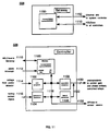
- the power delivery system 500 includes a splitter 502, a plurality of power amplifier modules 508-514, a gateway controller 506, and a power combiner 504. Each of the power amplifier modules 508-514 are coupled to the splitter 502, the combiner 504 and the gateway controller 506.
- the splitter 502 is a power splitter, such as the splitter of FIGs. 1-4.
- the combiner 504 is preferably a power combiner, such as the combiner of FIGs. 1-4.
- the gateway controller 506 is preferably implemented as an embedded microprocessor controller, such as a Motorola 68360 or 68HC11.
- the power amplifier module 508 includes an input switch 520, a power detector 522, a variable attenuator 524, a power amplifier 526, an output switch 530, an alarm detector 532, and a control module 528.
- the control module 528 is coupled to the gateway controller 506 via a data interface 516.
- the control module 528 is also coupled to each of the other components in the power amplifier module 508.
- the input switch 520 is a SHS-080AG switch from Hitachi Metals America, Ltd, Arlington Heights, Illinois
- the output switch 530 is a RSS-SR001 relay -from RelComm Technologies, Inc., Salisbury, Maryland.
- the amplifier 526 is preferably a feedforward type of amplifier, such as the feedforward amplifier in a Motorola SC TM 9600 base station or as described in U.S. Pat. No. 5,307,022.
- the local control module 528 is preferably implemented as an embedded microprocessor controller, such as a Motorola 68360 or 68HC11.
- the power detector 522 is any suitable circuit that can detect a power level associated with the power amplifier 526, such as a power detection circuit for detecting the input power level of the power amplifier.
- FIG. 8 A detailed schematic of an example of such a power detector 522 is shown for illustration purposes in FIG. 8. Although the power detector 522 is shown within module 508, the power detector 522 may be located at many alternative positions in the system 500, such as at the RF input 544 or at the RF output 546.
- variable attenuator 524 may also be implemented with suitable circuit elements and an example of such a circuit is shown in FIG. 9. It should be understood that the variable attenuator may be placed at any position in the system 500 that is prior to the power amplifier 526, such as at the RF input 544.
- the alarm detector 532 includes a plurality of alarm sensors 1002, a plurality of digital to analog converters (D/A) 1004, a plurality of comparitors 1006, and a digital logic component, such as OR gate 1008.
- the alarm detector 532 receives alarm sensor inputs 1010, and alarm thresholds 1012 and produces an alarm interrupt 1014 indicating that an alarm condition has occurred.
- the alarm interrupt 1014 is fed to module controller 528, which sends an alarm message to the gateway controller 506 to inform the gateway 506 of the alarm.
- the alarm detector 532 is designed to detect faults that may be severe enough to remove a module from service.
- the sensors 1002 may be of various types depending on the type of fault to be detected and vary depending upon the particular application and implementation. The following list of suitable sensors is not exhaustive and is for illustrative purposes only: temperature alarm - Analog Devices TMP-01E, PT suppression alarm - RSSI voltage from Signetics SA604 receiver IC, overdrive or reflected power alarms - voltages from power detector of FIG. 8, synthesizer lock alarm - Motorola MC145200, and current alarm - current sensing resistor on each power amplifier stage.
- the controller 528 includes a microprocessor 1100, an analog to digital converter (A/D) 1102, a bank of A/D converters 1104, a bank of D/A converters 1106, and a bank of data latches 1108.
- the microprocessor 1100 receives an alarm interrupt input 1112, and communicates with the gateway controller 506 via a data bus, such as the HDLC bus 1110 and communicates with the alarm detector 532 via control bus 1132.
- A/D converter 1102 receives a voltage level from power detector input 1114 and the bank of A/D converters 1104 receives a tuning sensor input 1116.
- the microprocessor 1100 communicates with the A/D converter 1102, the bank of A/D converters 1104, the bank of D/A converters 1106, and the bank of data latches 1108 over the internal bus 1118.
- the bank of data latches produces an output 1122 which is combined with the output of the bank of D/A converters 1106 to produce analog output lines 1130.
- the analog output lines control the gain of the variable attenuator 524, the input switch 520, and the output switch 530 for each of the modules 508.
- An example of a suitable A/D converter 1104 is an Analog Devices AD7891 eight channel 12 bit A/D converter.
- a suitable D/A converter 1106 is an Analog Devices AD7804 four channel 10 bit DAC or an Analog Devices AD8403 four channel 8 bit RDAC for the D/A where an alarm threshold setting is needed.
- An example of a suitable bank of data latches 1108 is a Motorola 74HCT273A.
- the controller 528 also includes the conventional supporting circuits described below with reference to the gateway controller 506.
- the controller 528 performs many functions. For example, the controller 528 tracks its operation state and communicates with the gateway controller 506 to inform the gateway 506 of state transitions. The controller 506 also may be used to tune the power amplifiers 526, to monitor alarm sensors, and to control alarm thresholds. The controller 528, typically in response to the gateway controller 506, may open or close the input switch 520 or the output switch 530 and may adjust the gain of the variable attenuator 524.
- the gateway controller 506 includes a microprocessor 1150 and communicates with the controller 528 via HDLC bus 1110.
- the gateway controller 506 also communicates with a system controller via a data link 1152, such as an Ethernet connection.
- the system controller may be a mobile switching center in a cellular system.
- the gateway controller 506 coordinates operation of the other controllers 528 in each of the amplifier modules 508 by tracking operating states, calculating amplifier gain values and offsets, and determining what actions each controller 528 should take. Most of the actions for the sleep mode and module shed methods take place in the gateway controller 506.
- gateway controller 506 includes conventional supporting circuitry, such as memory, a clock, a reset switch, various input/output port interfaces, such as the HDLC bus and the Ethernet interface, and other digital support logic to buffer and otherwise handle the various signals and components of the system.
- conventional supporting circuitry such as memory, a clock, a reset switch, various input/output port interfaces, such as the HDLC bus and the Ethernet interface, and other digital support logic to buffer and otherwise handle the various signals and components of the system.
- an RF input signal 544 is split by splitter 502 into a plurality of signals 518 which are input to each of the plurality of power amplifier modules 508, 510, 512, 514.
- the split signals 518 are each amplified by the respective power amplifier module 508-514 and output as amplified signals 540.
- the amplified signals 540 are then combined by combiner 504 into an RF output signal 546.
- the number of active power amplifiers may be modified with an acceptable level of change in the overall power gain of the system 500.
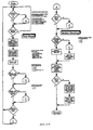
- one of the power amplifier modules 508-514 detects an alarm condition, such as via alarm detector 532 in module 508, that affects the service of that module.
- the control module 528 may detect an alarm condition either by routinely polling the alarm detectors 532, or by an interrupt input from the alarm detectors 532.
- the affected module sends an alarm message to the gateway controller 506, at step 604.
- the gateway controller 606 sends a message to the other modules instructing them to reduce their power gain by a level determined by the controller 606.
- the following formula may be used to determine the amount of gain reduction: 10 * LOG ( original number of modules in service / number of modules remaining in service after faulty module ( s ) removed ) module(s) removed)
- the above formula gives the ideal power gain, due to inherent imperfections in circuit elements, it may be desirable to offset the ideal calculated value. For example, where there are four modules and one is to be removed, the ideal level of gain reduction is 1.25 dB, but an offset, such as an offset of .25 dB may be applied so that the total gain reduction of each of the other modules is at least about 1.25 dB and preferably about 1.5 dB.
- the non-affected modules respond to the gateway 506 after they have successfully reduced their gain, at step 608.
- the modules 508-514 may reduce their gain by changing the attenuation level at the variable attenuator 524.
- the gateway controller 506 sends a message to the faulty module to open its input and output switches 520, 530, to remove that module from service.
- the faulty module then informs the gateway controller 506 that it has shut down, at step 612, performs diagnostic testing to determine the cause of the fault, and stores the results of the diagnostic testing in a non-volatile memory for future use, such as by factory personnel, at step 614.
- the gateway controller 506 sends a message to a system controller, such as a mobile switching center or a mobility manager in a cellular system, of the alarm condition.
- the above alarm control strategy permits implementation of a power amplifier system that performs at a high power gain level under at least three different conditions.
- an alarm is not active and the system maximum traffic load is less than the maximum capability of the system. This is normal operation, and a sleep mode method, described in further detail below, can be used to improve efficiency.
- a sleep mode method described in further detail below.
- an alarm exists but the system maximum traffic load is less than the maximum capability of the system with the alarmed module removed from service. When the fault is detected, the alarmed module is removed from service.
- the above alarm control strategy allows the power delivery system to remain in service with negligible effect to the power gain of the power delivery system.
- the sleep mode method can still be used to improve efficiency even when the alarmed module is remove from service.
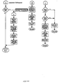
- FIG. 7 another embodiment of a method of controlling a power delivery system, such as the power delivery system 500 of FIG. 5, is illustrated.
- the method includes the steps of determining whether to place a given module into a sleep mode.
- sleep mode one or more power amplifiers are taken out of service temporarily to allow the power amplifier system 500 to operate more efficiently with lower operating costs.
- the sleep mode may be used in off times when- traffic requirements are low.
- In-sleep mode the module is removed from service by opening the input switch 520 and the output switch 530.
- at least some of the DC power dissipating circuits in the amplifier 526 are shut off.
- the control module 528 typically remains active so that tuning parameters of the amplifier 526 are quickly available after the module is awakened.
- the gateway checks to determine if any of the modules are in a sleep time interval.
- One method of providing a sleep time interval is to store general traffic loading conditions based on time of day into the gateway. In this case, a sleep interval would occur at times during the day when traffic is lightest, such as during the early morning hours (e.g. 1-4 A.M.). If the sleep window condition passes, the status of alarms is checked, at step 704. If there are alarms, then processing proceeds as described in FIG. 6. Otherwise, the gateway sends a message to the modules to enable a sleep mode interrupt to allow for sleep mode.
- each of the modules monitor traffic levels, such by monitoring input power readings from the power detector, compare the readings to a threshold, and send messages back to the gateway when thresholds are exceeded.
- the gateway determines the number of modules to put to sleep and the number to wake up based on sleep messages and wakeup messages from the modules. In the particular example of FIG. 7, steps 710-720, the gateway puts two of the four modules to sleep and then wakes up both modules if any wakeup message is received. However, It is contemplated that many other combinations of modules put to sleep or woken up based on the thresholds and messages received by the gateway are possible depending on the particular application.
- step 722 if the sleep window has ended or any alarm conditions are detected, all modules are woken up, at step 724, and the gateway sends a message to all modules to disable sleep interrupts. Otherwise, processing for steps 710-720 is repeated.
- the method of controlling the power delivery system 500 has been described separately with respect to a specific module shedding method in FIG. 6 and a specific sleep mode method in FIG. 7, it is possible, and in some applications preferable, to use a combination of both of the methods.
- certain criteria such as power level or alarm conditions may be used to determine when to enter and leave the sleep mode
- many other sleep criteria may be used. For example, the number of modules in sleep mode, whether the module is below a sleep low threshold or above a sleep high threshold, and whether a particular module is in service or out of service.
- FIG. 12A and FIG. 12B A detailed flow chart of an example of a method of controlling a power delivery system using a combination of both module shedding and sleep mode as well as a variety of sleep mode criteria is shown in FIG. 12A and FIG. 12B.
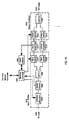
- the power delivery system includes an input splitter 1318, a gateway controller 1300, an alarm detector 1302, power amplifiers 1312, and an output combiner 1320.
- the input splitter 1318 includes a variable attenuator 1304, a power detector 1306, a power splitter 1308, and a first and a second input switch 1310.
- the variable attenuator 1304 receives an RF input signal 1322.
- the power detector 1306 is in communication with the gateway controller 1300, and the input switches 1310 are each coupled to a respective power amplifier 1312.
- the output combiner 1320 includes first and second output switches 1314 and a power combiner 1316.
- the output switches 1314 are each coupled to a respective power amplifier 1312.
- the combiner 1316 outputs an RF output signal 1324.
- the alarm detector 1302 is coupled to the power amplifiers 1312 and the gateway controller 1300.
- a single variable attenuator such as variable attenuator 1304, may be used to adjust the gain of more than one power amplifier 1312.
- the input switches 1310 are located at the input splitter 1318, instead of in power amplifier modules. By placing the input switches 1310 and the variable attenuator 1304 in the input splitter 1318 instead of in the various power amplifier modules, a local module controller, such as controller 528 of FIG. 5, is not needed. Instead, all of the control functions are performed in the common gateway controller 1300.
- each of the individual components disclosed in FIG. 13 is preferably the same as those described in further detail above in reference to FIG. 5.
- the power detector 1306 of FIG. 13 is preferably the same as the power detector 522 of FIG. 5 and FIG. 8.
- the method of controlling a power delivery system as described with reference to FIGs 6, 7, and 12 may be used with the system of FIG. 13 as well as with the system of FIG. 5.
- modules may be inactivated during times when full power is not needed, such as during low traffic times during the day. In this manner, the useful life of each module can be extended, improving efficiency and reducing costs of operation.
- Another potential benefit is that the system has great flexibility since modules may be physically added to the system, or an extra module could be added for high traffic periods or for redundancy purposes. In this case, the extra module would normally be in the sleep mode, i.e. inactive, but could be quickly activated if another module failed or if the traffic level exceeded the capacity of the other modules.
Landscapes
- Engineering & Computer Science (AREA)
- Power Engineering (AREA)
- Amplifiers (AREA)
- Transmitters (AREA)
- Supply And Distribution Of Alternating Current (AREA)
Applications Claiming Priority (3)
| Application Number | Priority Date | Filing Date | Title |
|---|---|---|---|
| US662573 | 1996-06-13 | ||
| US08/662,573 US5831479A (en) | 1996-06-13 | 1996-06-13 | Power delivery system and method of controlling the power delivery system for use in a radio frequency system |
| PCT/US1997/006163 WO1997048181A1 (en) | 1996-06-13 | 1997-04-16 | Power delivery system and method of controlling the power delivery system for use in a radio frequency system |
Publications (3)
| Publication Number | Publication Date |
|---|---|
| EP0904633A1 EP0904633A1 (en) | 1999-03-31 |
| EP0904633A4 EP0904633A4 (en) | 2001-12-05 |
| EP0904633B1 true EP0904633B1 (en) | 2006-10-18 |
Family
ID=24658269
Family Applications (1)
| Application Number | Title | Priority Date | Filing Date |
|---|---|---|---|
| EP97921176A Expired - Lifetime EP0904633B1 (en) | 1996-06-13 | 1997-04-16 | Power delivery system and method of controlling the power delivery system for use in a radio frequency system |
Country Status (8)
Families Citing this family (56)
| Publication number | Priority date | Publication date | Assignee | Title |
|---|---|---|---|---|
| US6463269B2 (en) * | 1997-03-31 | 2002-10-08 | Bellsouth Corporation | Power amplification system with intelligent control of amplifier modules |
| US6292677B1 (en) * | 1997-06-26 | 2001-09-18 | Motorola, Inc. | Power delivery system and method of controlling the power delivery system for use in a radio frequency system |
| DE19730086A1 (de) * | 1997-07-14 | 1999-01-21 | Bosch Gmbh Robert | Sendeeinrichtung für Hochfrequenzsignale |
| KR100241780B1 (ko) * | 1997-12-16 | 2000-02-01 | 윤종용 | 무선 통신 단말기의 전원 절약 장치 |
| US6182231B1 (en) * | 1998-03-31 | 2001-01-30 | International Business Machines Corporation | Dynamic program suspension |
| US6128479A (en) * | 1998-06-04 | 2000-10-03 | Motorola, Inc. | Radio frequency amplifier structure |
| US5999046A (en) * | 1998-06-10 | 1999-12-07 | Motorola, Inc. | Power combiner for use in a radio frequency system and a method of constructing a power combiner |
| US6252871B1 (en) * | 1998-07-01 | 2001-06-26 | Powerwave Technologies, Inc. | Switchable combiner/splitter |
| US6094097A (en) * | 1998-08-11 | 2000-07-25 | Lucent Technologies, Inc. | Programmable RF power combiner |
| US6424216B2 (en) * | 1998-08-19 | 2002-07-23 | Harris Corporation | Power amplifier system having amplifier failure compensation |
| US6124758A (en) * | 1998-08-19 | 2000-09-26 | Harris Corporation | RF power amplifier control system |
| US6188277B1 (en) * | 1998-08-19 | 2001-02-13 | Harris Corporation | Power amplifier having monitoring and circuit protection |
| US6799020B1 (en) | 1999-07-20 | 2004-09-28 | Qualcomm Incorporated | Parallel amplifier architecture using digital phase control techniques |
| US6346744B1 (en) * | 1999-09-14 | 2002-02-12 | Sarnoff Corporation | Integrated RF M×N switch matrix |
| US6255903B1 (en) | 1999-12-06 | 2001-07-03 | Motorola | Linear power amplifier with configurable feedforward error correction circuits |
| US6587013B1 (en) | 2000-02-16 | 2003-07-01 | Signal Technology Corporation | RF power combiner circuit with spaced capacitive stub |
| US6711388B1 (en) * | 2000-03-30 | 2004-03-23 | Nokia Corporation | Distributed power level control system of transmitter for cellular communication |
| FR2812141B1 (fr) * | 2000-07-21 | 2003-01-10 | Thomson Multimedia Sa | Bloc d'amplification de signaux rf, dispositif d'emission de signaux rf et terminal-antenne d'emission de signaux rf |
| TW503345B (en) * | 2001-03-26 | 2002-09-21 | Mediatec Inc | Power controller |
| US7133921B2 (en) * | 2001-04-06 | 2006-11-07 | Mks Instruments, Inc. | Portable devices for different control interfaces |
| US6778921B2 (en) | 2001-04-06 | 2004-08-17 | Eni Technology, Inc. | Modular architecture for industrial power delivery system |
| US6819173B2 (en) * | 2001-04-19 | 2004-11-16 | Motorola, Inc. | Method and apparatus for reduction of distortion in a transmitter |
| US6744316B2 (en) | 2001-04-19 | 2004-06-01 | Motorola, Inc. | Method and apparatus far reduction of distortion in a transmitter |
| US6650200B2 (en) * | 2001-04-20 | 2003-11-18 | Anaren Microwave, Inc. | Dynamic combiner/splitter for RF signal systems |
| US8811917B2 (en) | 2002-05-01 | 2014-08-19 | Dali Systems Co. Ltd. | Digital hybrid mode power amplifier system |
| US8380143B2 (en) | 2002-05-01 | 2013-02-19 | Dali Systems Co. Ltd | Power amplifier time-delay invariant predistortion methods and apparatus |
| US7092681B2 (en) * | 2002-07-23 | 2006-08-15 | Broadcom Corporation | High output power radio frequency integrated circuit |
| US8190163B2 (en) | 2002-08-08 | 2012-05-29 | Qualcomm Incorporated | Methods and apparatus of enhanced coding in multi-user communication systems |
| US7363039B2 (en) | 2002-08-08 | 2008-04-22 | Qualcomm Incorporated | Method of creating and utilizing diversity in multiple carrier communication system |
| US6961595B2 (en) | 2002-08-08 | 2005-11-01 | Flarion Technologies, Inc. | Methods and apparatus for operating mobile nodes in multiple states |
| GB2395077A (en) * | 2002-11-01 | 2004-05-12 | N & L Ltd | An amplifier arrangement linearised by predistortion and feedforward; adaptive bias for improved efficiency; thermal overload protection |
| KR101061654B1 (ko) | 2003-02-19 | 2011-09-01 | 콸콤 인코포레이티드 | 멀티-유저 통신 시스템들에서 제어된 중첩 코딩 |
| US7269036B2 (en) * | 2003-05-12 | 2007-09-11 | Siemens Vdo Automotive Corporation | Method and apparatus for adjusting wakeup time in electrical power converter systems and transformer isolation |
| US8593932B2 (en) | 2003-05-16 | 2013-11-26 | Qualcomm Incorporated | Efficient signal transmission methods and apparatus using a shared transmission resource |
| TWI277308B (en) * | 2003-08-07 | 2007-03-21 | Nokia Corp | Method and apparatus for discrete power synthesis of multicarrier signals with constant envelope power amplifiers |
| US7925291B2 (en) | 2003-08-13 | 2011-04-12 | Qualcomm Incorporated | User specific downlink power control channel Q-bit |
| US7343138B2 (en) * | 2003-12-08 | 2008-03-11 | M/A-Com, Inc. | Compensating for load pull in electromagentic signal propagation using adaptive impedance matching |
| US8125572B2 (en) * | 2005-03-15 | 2012-02-28 | Maxim Integrated Products, Inc. | System and method for automatic power-up and power-down of an output video circuit |
| US7221223B2 (en) * | 2005-07-28 | 2007-05-22 | Motorola, Inc. | Methods and apparatus of managing a power amplifier |
| US7221222B2 (en) * | 2005-07-28 | 2007-05-22 | Motorola, Inc. | Methods and apparatus of managing a power amplifier |
| JP4545089B2 (ja) * | 2005-12-27 | 2010-09-15 | シャープ株式会社 | 画像記録システム及びプログラム |
| US8004364B2 (en) * | 2006-12-22 | 2011-08-23 | The United States Of America As Represented By The Administrator Of The National Aeronautics And Space Administration | High power RF solid state power amplifier system |
| WO2008078195A2 (en) | 2006-12-26 | 2008-07-03 | Dali Systems Co., Ltd. | Method and system for baseband predistortion linearization in multi-channel wideband communication systems |
| PL3410785T3 (pl) | 2007-01-11 | 2025-06-09 | Qualcomm Incorporated | Zastosowanie dtx i drx w systemie łączności bezprzewodowej |
| WO2008111172A1 (ja) * | 2007-03-13 | 2008-09-18 | Panasonic Corporation | 電力増幅器 |
| DE102008016154B4 (de) * | 2008-03-28 | 2013-08-08 | Eads Deutschland Gmbh | Verfahren zur Kompensation von Verstärkungsänderungen bei einer Verstärkerschaltung |
| US7817559B2 (en) * | 2008-04-11 | 2010-10-19 | Nokia Siemens Networks Oy | Network node power conservation apparatus, system, and method |
| TW201019654A (en) * | 2008-11-10 | 2010-05-16 | Inst Information Industry | Control apparatus, signal transmission method and computer program product for the control apparatus |
| US8344704B2 (en) * | 2008-12-31 | 2013-01-01 | Advanced Energy Industries, Inc. | Method and apparatus for adjusting the reference impedance of a power generator |
| FR2937207A1 (fr) * | 2009-03-05 | 2010-04-16 | Thomson Licensing | Emetteur rf de puissance comportant un systeme de regulation de puissance et methode de regulation a une puissance requise d'un signal de sortie rf d'un emetteur de puissance |
| EP2430531B1 (en) * | 2009-04-24 | 2019-12-04 | Dali Systems Co. Ltd. | Remotely reconfigurable power amplifier system and method |
| CN105208083B (zh) | 2010-09-14 | 2018-09-21 | 大力系统有限公司 | 用于发送信号的系统和分布式天线系统 |
| US8902015B1 (en) | 2011-11-18 | 2014-12-02 | The United States Of America As Represented By The Administrator Of The National Aeronautics And Space Administration | Radio frequency power load and associated method |
| JP5873466B2 (ja) * | 2013-08-23 | 2016-03-01 | 株式会社Nttドコモ | マルチアンテナアレーシステム |
| JP6686282B2 (ja) * | 2015-03-16 | 2020-04-22 | セイコーエプソン株式会社 | 回路装置、物理量検出装置、電子機器及び移動体 |
| FR3044494B1 (fr) * | 2015-11-30 | 2019-10-11 | Thales | Circuit de commutation, etage et appareil d'amplification et/ou de division associes |
Family Cites Families (8)
| Publication number | Priority date | Publication date | Assignee | Title |
|---|---|---|---|---|
| US3072858A (en) * | 1959-07-22 | 1963-01-08 | Sperry Rand Corp | Redundant amplifier failure alarm |
| JPS56112106A (en) * | 1980-02-09 | 1981-09-04 | Nec Corp | High frequency power amplifier |
| US4298844A (en) * | 1980-03-21 | 1981-11-03 | Comsonics, Inc. | Split-band redundant amplifier system |
| CA1266707A (en) * | 1985-12-16 | 1990-03-13 | Steve S. Yang | Method of calibrating and equalizing a multi-channel automatic gain control amplifier |
| US4780685A (en) * | 1987-03-19 | 1988-10-25 | General Electric Company | Composite power amplifier with redundancy |
| US5025225A (en) * | 1989-12-15 | 1991-06-18 | Raytheon Company | Amplifier having substantially constant D.C. to r.f. conversion efficiency |
| JPH0454006A (ja) * | 1990-06-22 | 1992-02-21 | Fujitsu Ltd | 増幅装置 |
| JPH05121916A (ja) * | 1991-10-29 | 1993-05-18 | Japan Radio Co Ltd | 高周波電力分配・合成回路 |
-
1996
- 1996-06-13 US US08/662,573 patent/US5831479A/en not_active Expired - Lifetime
-
1997
- 1997-02-14 US US08/799,967 patent/US5867060A/en not_active Expired - Lifetime
- 1997-04-16 JP JP10501579A patent/JP2000512107A/ja active Pending
- 1997-04-16 KR KR1019980710217A patent/KR100345393B1/ko not_active Expired - Fee Related
- 1997-04-16 WO PCT/US1997/006163 patent/WO1997048181A1/en active IP Right Grant
- 1997-04-16 AU AU27291/97A patent/AU2729197A/en not_active Abandoned
- 1997-04-16 CA CA002257954A patent/CA2257954C/en not_active Expired - Fee Related
- 1997-04-16 DE DE69736830T patent/DE69736830T2/de not_active Expired - Lifetime
- 1997-04-16 EP EP97921176A patent/EP0904633B1/en not_active Expired - Lifetime
Also Published As
| Publication number | Publication date |
|---|---|
| EP0904633A4 (en) | 2001-12-05 |
| CA2257954C (en) | 2001-08-14 |
| CA2257954A1 (en) | 1997-12-18 |
| DE69736830T2 (de) | 2007-05-10 |
| US5831479A (en) | 1998-11-03 |
| DE69736830D1 (de) | 2006-11-30 |
| US5867060A (en) | 1999-02-02 |
| AU2729197A (en) | 1998-01-07 |
| EP0904633A1 (en) | 1999-03-31 |
| KR100345393B1 (ko) | 2002-09-18 |
| KR20000016621A (ko) | 2000-03-25 |
| WO1997048181A1 (en) | 1997-12-18 |
| JP2000512107A (ja) | 2000-09-12 |
Similar Documents
| Publication | Publication Date | Title |
|---|---|---|
| EP0904633B1 (en) | Power delivery system and method of controlling the power delivery system for use in a radio frequency system | |
| US6124758A (en) | RF power amplifier control system | |
| EP2197128B1 (en) | Systems and methods for implementing fully redundant antenna hopping with multi-carrier power amplifiers and combing schemes within a base station | |
| EP0670630A1 (en) | Amplifier system | |
| EP0972339B1 (en) | Power amplication system with intelligent control of amplifier modules | |
| US6002928A (en) | Switching apparatus and method for transceiver of cellular base station in code division multiple access mobile telecommunication system | |
| US5548799A (en) | Mobile communication system having a control for limiting the number of carriers based on the level of intermodulation distortion | |
| JPH0252512A (ja) | 電力増幅装置 | |
| US6181929B1 (en) | Method for switching cell site controllers | |
| US6937387B1 (en) | System and method for automatic recovery from a control loop failure | |
| JP2891962B2 (ja) | 電源制御装置 | |
| JPH05304429A (ja) | 並列運転増幅器とその異常検出回路 | |
| JP3755688B2 (ja) | 電動機制御装置 | |
| JPH06152265A (ja) | マイクロ波増幅装置 | |
| JP3042511B2 (ja) | 通信システムと該通信システムの外部送信出力停止方法 | |
| JPH0670297A (ja) | Catv用ステータスモニタによる自動利得制御回路の制御方法 | |
| JPS62188406A (ja) | 電力増幅回路 | |
| JPH02166931A (ja) | 警報信号選択回路 | |
| JPS63197128A (ja) | 送信チヤネル切換装置 | |
| JPH0260236A (ja) | 送受信切替方式 | |
| JPH0653944A (ja) | 回線切替制御方式 | |
| KR20000002440A (ko) | 개인 휴대 통신 서비스 기지국 시스템에서의 채널 엘리먼트 장애 처리 방법 | |
| KR20000043956A (ko) | 원방 감시 제어 시스템 | |
| KR20030075093A (ko) | 무선 전송 시스템의 송신부 절체 방법 | |
| JPH04137834A (ja) | 予備回路自己監視装置 |
Legal Events
| Date | Code | Title | Description |
|---|---|---|---|
| PUAI | Public reference made under article 153(3) epc to a published international application that has entered the european phase |
Free format text: ORIGINAL CODE: 0009012 |
|
| 17P | Request for examination filed |
Effective date: 19990113 |
|
| AK | Designated contracting states |
Kind code of ref document: A1 Designated state(s): DE FI GB SE |
|
| RIC1 | Information provided on ipc code assigned before grant |
Free format text: 7H 03F 3/68 A, 7H 03F 1/14 B, 7H 03F 1/52 B, 7H 03F 3/21 B |
|
| RIC1 | Information provided on ipc code assigned before grant |
Free format text: 7H 03F 3/68 A, 7H 03F 1/14 B, 7H 03F 1/52 B, 7H 03F 3/21 B, 7H 03F 1/02 B |
|
| A4 | Supplementary search report drawn up and despatched |
Effective date: 20011019 |
|
| AK | Designated contracting states |
Kind code of ref document: A4 Designated state(s): DE FI GB SE |
|
| 17Q | First examination report despatched |
Effective date: 20040123 |
|
| GRAP | Despatch of communication of intention to grant a patent |
Free format text: ORIGINAL CODE: EPIDOSNIGR1 |
|
| GRAS | Grant fee paid |
Free format text: ORIGINAL CODE: EPIDOSNIGR3 |
|
| GRAA | (expected) grant |
Free format text: ORIGINAL CODE: 0009210 |
|
| AK | Designated contracting states |
Kind code of ref document: B1 Designated state(s): DE FI GB SE |
|
| REG | Reference to a national code |
Ref country code: GB Ref legal event code: FG4D |
|
| REF | Corresponds to: |
Ref document number: 69736830 Country of ref document: DE Date of ref document: 20061130 Kind code of ref document: P |
|
| REG | Reference to a national code |
Ref country code: SE Ref legal event code: TRGR |
|
| PLBE | No opposition filed within time limit |
Free format text: ORIGINAL CODE: 0009261 |
|
| STAA | Information on the status of an ep patent application or granted ep patent |
Free format text: STATUS: NO OPPOSITION FILED WITHIN TIME LIMIT |
|
| 26N | No opposition filed |
Effective date: 20070719 |
|
| REG | Reference to a national code |
Ref country code: GB Ref legal event code: 732E Free format text: REGISTERED BETWEEN 20110127 AND 20110202 |
|
| REG | Reference to a national code |
Ref country code: DE Ref legal event code: R081 Ref document number: 69736830 Country of ref document: DE Owner name: MOTOROLA MOBILITY, INC. ( N.D. GES. D. STAATES, US Free format text: FORMER OWNER: MOTOROLA INC., SCHAUMBURG, ILL., US Effective date: 20110324 Ref country code: DE Ref legal event code: R081 Ref document number: 69736830 Country of ref document: DE Owner name: MOTOROLA MOBILITY, INC. ( N.D. GES. D. STAATES, US Free format text: FORMER OWNER: MOTOROLA INC., SCHAUMBURG, US Effective date: 20110324 |
|
| PGFP | Annual fee paid to national office [announced via postgrant information from national office to epo] |
Ref country code: GB Payment date: 20150427 Year of fee payment: 19 Ref country code: SE Payment date: 20150429 Year of fee payment: 19 Ref country code: DE Payment date: 20150429 Year of fee payment: 19 Ref country code: FI Payment date: 20150429 Year of fee payment: 19 |
|
| REG | Reference to a national code |
Ref country code: DE Ref legal event code: R119 Ref document number: 69736830 Country of ref document: DE |
|
| REG | Reference to a national code |
Ref country code: SE Ref legal event code: EUG |
|
| GBPC | Gb: european patent ceased through non-payment of renewal fee |
Effective date: 20160416 |
|
| PG25 | Lapsed in a contracting state [announced via postgrant information from national office to epo] |
Ref country code: FI Free format text: LAPSE BECAUSE OF NON-PAYMENT OF DUE FEES Effective date: 20160416 Ref country code: GB Free format text: LAPSE BECAUSE OF NON-PAYMENT OF DUE FEES Effective date: 20160416 Ref country code: DE Free format text: LAPSE BECAUSE OF NON-PAYMENT OF DUE FEES Effective date: 20161101 |
|
| PG25 | Lapsed in a contracting state [announced via postgrant information from national office to epo] |
Ref country code: SE Free format text: LAPSE BECAUSE OF NON-PAYMENT OF DUE FEES Effective date: 20160417 |
|
| P01 | Opt-out of the competence of the unified patent court (upc) registered |
Effective date: 20230520 |