EP0903849B1 - Circuit compresseur du niveau audio - Google Patents
Circuit compresseur du niveau audio Download PDFInfo
- Publication number
- EP0903849B1 EP0903849B1 EP98117245A EP98117245A EP0903849B1 EP 0903849 B1 EP0903849 B1 EP 0903849B1 EP 98117245 A EP98117245 A EP 98117245A EP 98117245 A EP98117245 A EP 98117245A EP 0903849 B1 EP0903849 B1 EP 0903849B1
- Authority
- EP
- European Patent Office
- Prior art keywords
- feedback
- differential amplifier
- output signal
- output
- comparator
- Prior art date
- Legal status (The legal status is an assumption and is not a legal conclusion. Google has not performed a legal analysis and makes no representation as to the accuracy of the status listed.)
- Expired - Lifetime
Links
- 230000006835 compression Effects 0.000 title claims description 21
- 238000007906 compression Methods 0.000 title claims description 21
- 230000005236 sound signal Effects 0.000 description 7
- 238000013459 approach Methods 0.000 description 3
- 238000010586 diagram Methods 0.000 description 1
- 239000004973 liquid crystal related substance Substances 0.000 description 1
Images
Classifications
-
- H—ELECTRICITY
- H03—ELECTRONIC CIRCUITRY
- H03G—CONTROL OF AMPLIFICATION
- H03G7/00—Volume compression or expansion in amplifiers
- H03G7/06—Volume compression or expansion in amplifiers having semiconductor devices
- H03G7/08—Volume compression or expansion in amplifiers having semiconductor devices incorporating negative feedback
-
- H—ELECTRICITY
- H03—ELECTRONIC CIRCUITRY
- H03F—AMPLIFIERS
- H03F3/00—Amplifiers with only discharge tubes or only semiconductor devices as amplifying elements
- H03F3/45—Differential amplifiers
- H03F3/45071—Differential amplifiers with semiconductor devices only
- H03F3/45076—Differential amplifiers with semiconductor devices only characterised by the way of implementation of the active amplifying circuit in the differential amplifier
- H03F3/4508—Differential amplifiers with semiconductor devices only characterised by the way of implementation of the active amplifying circuit in the differential amplifier using bipolar transistors as the active amplifying circuit
- H03F3/45085—Long tailed pairs
- H03F3/45094—Folded cascode stages
Definitions
- This invention relates to a level compression circuit which compresses the level of an audio signal.
- it relates to a level compression circuit in which a signal waveform is not significantly distorted when a signal is compressed.
- camcorders In which a magnetic tape is used to record video and sound signals. Such camcorders are equipped with a small built-in monitor such as a liquid crystal display. An image is played back on this monitor and sound is reproduced on a small speaker.
- a small built-in monitor such as a liquid crystal display. An image is played back on this monitor and sound is reproduced on a small speaker.
- first and second comparators compare the levels of the upper and lower ends of an output signal from a feedback differential amplifier with separate reference values. Output signals of the first and second comparator are applied to a feedback resistor of the feedback differential amplifier, and thus, the level of an input signal can be compressed while preserving its natural waveform.
- the present invention prevents offensive signal distortions even when an input signal level entering a camcorder play-back or similar circuit increases suddenly.
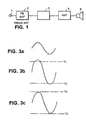
- Figure 1 is a partial block diagram of a conventional camcorder audio play-back system.
- Figure 2 shows the level compression circuit of the present invention.
- Figures 3(a) - 3(c) depict waveforms, which are used to explain the level compression circuit of the present invention in comparison with a prior art amplitiude limiter.
- FIG. 1 A portion of a prior art audio play-back circuit is shown in Figure 1.
- a reproduced audio signal is applied to an input terminal 1 and amplified by a Play-Back (PB) amplifier 2.
- PB Play-Back
- An operator adjusts the level of an amplified and adjusted signal with an electronic volume control circuit 3.
- An adjusted signal is amplified by a speaker amplifier 4 and supplied to a speaker 5.
- the operator who is playing back sound on the camcorder, can listen to the sound at a desired audio volume using the electronic volume control circuit 3.
- Such circuits typically have the distortion problem described in the Background of the Invention above.
- a feedback differential amplifier 10 amplifies an input signal, shown in Figure 3(a), and feeds back an output signal through feedback resistors 11 and 12.
- a first comparator 13 compares the level of the upper end of the output signal from the feedback differential amplifier 10 with a first reference value and generates a first differential current.
- a second comparator 14 compares the level of the lower end of the output signal from said feedback differential amplifier with a second reference value and generates a second differential current.
- a transistor 16 is a component of the feedback differential amplifier 10, which functions as a speaker amplifier.
- An audio signal from a signal source 15 is applied to the base of the transistor 16 and amplified.
- the amplified signal appears on an output terminal 17 of the feedback differential amplifier 10.
- the voltage of this signal is divided by the feedback resistors 11 and 12, and fed back to the base of a transistor 18.
- the resistance ratio of the feedback resistors 11 and 12 determines the gain of the feedback differential amplifier 10.
- the signal which appears on the output terminal 17 of the feedback differential amplifier 10 is applied to a first and second comparator 13 and 14, so that compression is performed.
- the voltage V1 of a first reference source 19, depicted as a battery, is set at a level V1 shown in Figure 3(c).
- the voltage V2 of a second reference source 20 is set at another level V2, as shown in Figure 3(c).
- a solid line in Figure 3(c) illustrates an audio signal.
- a transistor 24 is turned off. Hence, the collector current of the transistor 23 flows through the feedback resistor 11.
- the signal level appearing at the output terminal 17 of the feedback differential amplifier 10 is reduced. This is how the compression works when the output level approaches the voltage V1 of the first reference source 19. As the transistor 21 is driven harder, compression becomes more intensive. When the transistor 21 is completely turned on, the signal level reaches its maximum value (limited value).
- the signal amplitude is limited by controlling the DC voltage at the output terminal 17 in Figure 1. Even when the amplitude is compressed, a waveform remains natural.
- the slope of the positive waveform is determined by the values of resistors 28 and 29, connected to current source 30, and the slope of the negative waveform is determined by the values of resistors 31 and 32, connected to current source 33.
- the turned-off transistor 24 As illustrated in Figure 3(c), the voltage V2 of the second reference source 20 is set at a low level.
- a transistor 25 When the signal level appearing at the output terminal 17 of the feedback differential amplifier 10 is high, a transistor 25 is turned on and a transistor 26 is turned off. Thus, there is no current flowing through a current mirror circuit 27.
- the transistor 23 Under the current conditions, the transistor 23 is turned off. Hence, the collector current of the transistor 23 flows through the feedback resistor 11. In other words, this current flows in the opposite direction as that in the previous case and thus, the DC voltage at the output terminal 17 is increased by the voltage drop across the feedback resistor 11. In this manner, the signal amplitude is also limited at the lower end while the signal's natural waveform is preserved.
- Figure 3(b) illustrates a case in which a signal amplitude is limited in a simple manner, in accordance with prior art of the type mentioned in the Background of the Invention above.
- the circuit of the present invention allows the signal amplitude to be compressed while it preserves its natural waveform, as illustrated in Figure 3(c).
Landscapes
- Engineering & Computer Science (AREA)
- Power Engineering (AREA)
- Amplifiers (AREA)
- Tone Control, Compression And Expansion, Limiting Amplitude (AREA)
Claims (12)
- Circuit de compression de niveau audio pour produire un signal de sortie comprimé comportant :un amplificateur (10) différentiel de rétroaction connecté pour recevoir un signal d'entrée et pour envoyer en retour une partie de son signal de sortie par l'intermédiaire d'au moins une résistance (11, 12) de rétroaction,un premier comparateur (13) connecté pour recevoir le signal de sortie de l'amplificateur différentiel de rétroaction et une première valeur de référence, et produisant un premier signal de sortie comparateur représentatif de la différence entre le niveau de l'extrémité supérieure du signal de sortie de l'amplificateur différentiel de rétroaction et la première valeur de référence, etun second comparateur (14) connecté pour recevoir le signal de sortie de l'amplificateur différentiel de rétroaction et une seconde valeur de référence, et produisant un second signal de sortie comparateur représentatif de la différence entre le niveau de l'extrémité inférieure du signal de sortie de l'amplificateur différentiel de rétroaction et la seconde valeur de référence,les signaux de sortie de comparateur étant appliqués à la résistance de rétroaction, ajustant de manière automatique la sortie de l'amplificateur différentiel de rétroaction.
- Circuit de compression de niveau audio suivant la revendication 1, dans lequel ladite au moins une résistance de rétroaction comporte deux résistances connectées en série.
- Circuit de compression de niveau audio suivant la revendication 1, dans lequel les dispositifs actifs dans le circuit comportent des transistors, et dans lequel ladite au moins une résistance de rétroaction comporte deux résistances connectées en série pour former un diviseur de tension, une extrémité du diviseur étant connectée à la sortie du circuit et des comparateurs, et la connexion entre les deux résistances étant connectée à un transistor de l'amplificateur différentiel de rétroaction.
- Circuit de compression de niveau audio pour produire un signal de sortie comprimé comportant :un amplificateur (10) différentiel de rétroaction connecté pour recevoir un signal d'entrée et pour envoyer en retour une partie de son signal de sortie par l'intermédiaire d'au moins une résistance (11,12) de rétroaction,un premier comparateur (13) connecté pour recevoir le signal de sortie de l'amplificateur différentiel de rétroaction et une première valeur de référence, et produisant un premier courant différentiel, etun second comparateur (14) connecté pour recevoir le signal de sortie de l'amplificateur différentiel de rétroaction et une seconde valeur de référence, et produisant un second courant différentiel,les premier et second courants différentiels étant appliqués à la résistance de rétroaction, ajustant de manière automatique la sortie de l'amplificateur différentiel de rétroaction.
- Circuit de compression de niveau audio suivant la revendication 4, dans lequel ladite au moins une résistance de rétroaction comporte deux résistances connectées en série.
- Circuit de compression de niveau audio suivant la revendication 4, dans lequel des dispositifs actifs dans le circuit comportent des transistors, et ladite au moins une résistance de rétroaction comporte deux résistances connectées en série pour former un diviseur de tension, une extrémité du diviseur étant connectée à la sortie du circuit et des comparateurs, et la connexion entre les deux résistances étant connectée à un transistor de l'amplificateur différentiel de rétroaction.
- Circuit de compression de niveau comportant ;un amplificateur (10) différentiel de rétroaction pour amplifier un signal d'entrée et pour envoyer en retour des signaux de sortie par l'intermédiaire d'une résistance (11, 12) de rétroaction,un premier comparateur (13) pour comparer le niveau de l'extrémité supérieure d'un signal de sortie provenant de l'amplificateur différentiel de rétroaction à une première valeur de référence, etun second comparateur (14) pour comparer le niveau de l'extrémité inférieure du signal de sortie provenant de l'amplificateur différentiel de rétroaction à une seconde valeur de référence,le niveau du signal d'entrée étant comprimé en appliquant des signaux de sortie des premier et second comparateurs à la résistance de rétroaction, et en ajustant automatiquement la tension de courant continu de sortie de l'amplificateur différentiel de rétroaction.
- Circuit de compression de niveau audio suivant la revendication 7, dans lequel la résistance de rétroaction comporte deux parties connectées en série.
- Circuit de compression de niveau audio suivant la revendication 7, dans lequel des dispositifs actifs dans le circuit comportent des transistors, et dans lequel la résistance de rétroaction comporte deux parties connectées en série formant un diviseur de tension, une extrémité du diviseur étant connectée à la sortie du circuit et des comparateurs, et la connexion entre les deux parties étant connectée à un transistor de l'amplificateur différentiel e rétroaction.
- Circuit de compression de niveau comportantun amplificateur (10) différentiel de rétroaction pour amplifier un signal d'entrée et pour envoyer en retour des signaux par une résistance (11, 12) de rétroaction,un premier comparateur (13) pour comparer le niveau de l'extrémité supérieure d'un signal de sortie provenant de l'amplificateur différentiel de rétroaction à une première valeur de référence et pour produire un premier courant différentiel, etun second comparateur (14) pour comparer le niveau de l'extrémité inférieure du signal de sortie provenant de l'amplificateur différentiel de rétroaction à une seconde valeur de référence et pour produire un second courant différentiel,dans lequel le niveau du signal d'entrée est comprimé en appliquant les premier et second courants différentiels à la résistance de rétroaction de l'amplificateur différentiel de rétroaction, et en ajustant automatiquement la tension à courant continu de sortie de l'amplificateur différentiel de rétroaction.
- Circuit de compression de niveau audio suivant la revendication 10, dans lequel la résistance de rétroaction comporte deux parties connectées en série.
- Circuit de compression de niveau audio suivant la revendication 10, dans lequel des dispositifs actifs dans le circuit comportent des transistors, et dans lequel la résistance de rétroaction comporte deux parties connectées en série formant un diviseur de tension, une extrémité du diviseur étant connectée à la sortie du circuit et des comparateurs, et la connexion entre les deux parties étant connectée à un transistor de l'amplificateur différentiel de rétroaction.
Applications Claiming Priority (3)
| Application Number | Priority Date | Filing Date | Title |
|---|---|---|---|
| JP25358897 | 1997-09-18 | ||
| JP253588/97 | 1997-09-18 | ||
| JP9253588A JPH1197961A (ja) | 1997-09-18 | 1997-09-18 | レベル抑制回路 |
Publications (3)
| Publication Number | Publication Date |
|---|---|
| EP0903849A2 EP0903849A2 (fr) | 1999-03-24 |
| EP0903849A3 EP0903849A3 (fr) | 2000-02-16 |
| EP0903849B1 true EP0903849B1 (fr) | 2002-04-10 |
Family
ID=17253467
Family Applications (1)
| Application Number | Title | Priority Date | Filing Date |
|---|---|---|---|
| EP98117245A Expired - Lifetime EP0903849B1 (fr) | 1997-09-18 | 1998-09-11 | Circuit compresseur du niveau audio |
Country Status (6)
| Country | Link |
|---|---|
| US (1) | US6072365A (fr) |
| EP (1) | EP0903849B1 (fr) |
| JP (1) | JPH1197961A (fr) |
| KR (1) | KR100290994B1 (fr) |
| DE (1) | DE69804734T2 (fr) |
| TW (1) | TW437162B (fr) |
Families Citing this family (1)
| Publication number | Priority date | Publication date | Assignee | Title |
|---|---|---|---|---|
| JP2010119083A (ja) * | 2008-10-17 | 2010-05-27 | Denso Corp | 演算増幅器 |
Family Cites Families (11)
| Publication number | Priority date | Publication date | Assignee | Title |
|---|---|---|---|---|
| DE2906192A1 (de) * | 1979-02-17 | 1980-08-28 | Licentia Gmbh | Steuerspannungserzeuger fuer ein system zur dynamik-kompression und/oder -expansion |
| JPS5935522B2 (ja) * | 1979-10-16 | 1984-08-29 | ヤマハ株式会社 | 電力増幅器 |
| US4550426A (en) * | 1981-12-31 | 1985-10-29 | Motorola, Inc. | Method and means of detecting the presence of a signal representing voice and of compressing the level of the signal |
| EP0102945A1 (fr) * | 1982-03-04 | 1984-03-21 | Standard Telephones And Cables Public Limited Company | Circuits ecreteurs de formes d'ondes |
| US5014016A (en) * | 1989-04-13 | 1991-05-07 | Beltone Electronics Corporation | Switching amplifier |
| JPH04160910A (ja) * | 1990-10-25 | 1992-06-04 | Pioneer Electron Corp | 保護回路 |
| FR2700083B1 (fr) * | 1992-12-30 | 1995-02-24 | Gerard Perrot | Amplificateur à distorsion stable pour signaux audio. |
| JP2807853B2 (ja) * | 1993-01-29 | 1998-10-08 | リオン株式会社 | 出力回路 |
| JP3389334B2 (ja) * | 1993-07-28 | 2003-03-24 | 三洋電機株式会社 | 音声出力用集積回路 |
| US5596299A (en) * | 1995-05-30 | 1997-01-21 | Philips Electronics North America Corporation | IF amplifier/limiter with positive feedback |
| EP0763887B1 (fr) * | 1995-09-14 | 2000-03-22 | STMicroelectronics S.r.l. | Circuit de commande de gain automatique d'un amplificateur différentielle |
-
1997
- 1997-09-18 JP JP9253588A patent/JPH1197961A/ja active Pending
-
1998
- 1998-07-15 TW TW087111480A patent/TW437162B/zh not_active IP Right Cessation
- 1998-09-11 DE DE69804734T patent/DE69804734T2/de not_active Expired - Lifetime
- 1998-09-11 EP EP98117245A patent/EP0903849B1/fr not_active Expired - Lifetime
- 1998-09-17 US US09/156,798 patent/US6072365A/en not_active Expired - Lifetime
- 1998-09-17 KR KR1019980038385A patent/KR100290994B1/ko not_active Expired - Fee Related
Also Published As
| Publication number | Publication date |
|---|---|
| EP0903849A3 (fr) | 2000-02-16 |
| TW437162B (en) | 2001-05-28 |
| JPH1197961A (ja) | 1999-04-09 |
| KR19990029880A (ko) | 1999-04-26 |
| EP0903849A2 (fr) | 1999-03-24 |
| DE69804734T2 (de) | 2002-09-05 |
| KR100290994B1 (ko) | 2001-06-01 |
| DE69804734D1 (de) | 2002-05-16 |
| US6072365A (en) | 2000-06-06 |
Similar Documents
| Publication | Publication Date | Title |
|---|---|---|
| CA1305432C (fr) | Circuit de correction physiologique automatique | |
| US3986049A (en) | Audio compressor/limiter amplifier | |
| JP2000106511A (ja) | パワーアンプic | |
| US6975734B1 (en) | Audio apparatus of negative driving with adaptive gain control | |
| EP0903849B1 (fr) | Circuit compresseur du niveau audio | |
| US4823392A (en) | Compressor | |
| US3946249A (en) | Signal control circuit | |
| US6104818A (en) | Microphone circuit | |
| JPH04365210A (ja) | 車載音響再生装置 | |
| KR100213073B1 (ko) | 재생 오디오 신호의 주파수 특성 보상 장치 | |
| US5701353A (en) | Audio signal processing circuit for compressing or expanding audio signal in which output DC voltage is controlled in response to reference voltage | |
| US7460674B2 (en) | Audio effector circuit | |
| JPH0349503Y2 (fr) | ||
| JPH0279605A (ja) | オーディオ増幅器 | |
| JPH0419883Y2 (fr) | ||
| JP2594642B2 (ja) | 増幅回路 | |
| JPH0584119B2 (fr) | ||
| JPH0615331U (ja) | 増幅装置 | |
| JP3162869B2 (ja) | 記録再生装置のノイズ低減回路 | |
| JP2547732B2 (ja) | リミッタ回路 | |
| JPH10284964A (ja) | 音量調節装置 | |
| JPH10270962A (ja) | 自動音声出力可変装置 | |
| JPH11103224A (ja) | レベル抑制回路 | |
| JPH041525B2 (fr) | ||
| KR200159335Y1 (ko) | 재생 등화기의 자동 화질보상회로 |
Legal Events
| Date | Code | Title | Description |
|---|---|---|---|
| PUAI | Public reference made under article 153(3) epc to a published international application that has entered the european phase |
Free format text: ORIGINAL CODE: 0009012 |
|
| AK | Designated contracting states |
Kind code of ref document: A2 Designated state(s): DE FR GB NL |
|
| AX | Request for extension of the european patent |
Free format text: AL;LT;LV;MK;RO;SI |
|
| PUAL | Search report despatched |
Free format text: ORIGINAL CODE: 0009013 |
|
| AK | Designated contracting states |
Kind code of ref document: A3 Designated state(s): AT BE CH CY DE DK ES FI FR GB GR IE IT LI LU MC NL PT SE |
|
| AX | Request for extension of the european patent |
Free format text: AL;LT;LV;MK;RO;SI |
|
| 17P | Request for examination filed |
Effective date: 20000725 |
|
| AKX | Designation fees paid |
Free format text: DE FR GB NL |
|
| GRAG | Despatch of communication of intention to grant |
Free format text: ORIGINAL CODE: EPIDOS AGRA |
|
| 17Q | First examination report despatched |
Effective date: 20001228 |
|
| GRAG | Despatch of communication of intention to grant |
Free format text: ORIGINAL CODE: EPIDOS AGRA |
|
| GRAH | Despatch of communication of intention to grant a patent |
Free format text: ORIGINAL CODE: EPIDOS IGRA |
|
| GRAH | Despatch of communication of intention to grant a patent |
Free format text: ORIGINAL CODE: EPIDOS IGRA |
|
| REG | Reference to a national code |
Ref country code: GB Ref legal event code: IF02 |
|
| GRAA | (expected) grant |
Free format text: ORIGINAL CODE: 0009210 |
|
| AK | Designated contracting states |
Kind code of ref document: B1 Designated state(s): DE FR GB NL |
|
| REF | Corresponds to: |
Ref document number: 69804734 Country of ref document: DE Date of ref document: 20020516 |
|
| ET | Fr: translation filed | ||
| PLBE | No opposition filed within time limit |
Free format text: ORIGINAL CODE: 0009261 |
|
| STAA | Information on the status of an ep patent application or granted ep patent |
Free format text: STATUS: NO OPPOSITION FILED WITHIN TIME LIMIT |
|
| 26N | No opposition filed |
Effective date: 20030113 |
|
| PGFP | Annual fee paid to national office [announced via postgrant information from national office to epo] |
Ref country code: NL Payment date: 20130912 Year of fee payment: 16 |
|
| PGFP | Annual fee paid to national office [announced via postgrant information from national office to epo] |
Ref country code: FR Payment date: 20130826 Year of fee payment: 16 Ref country code: GB Payment date: 20130827 Year of fee payment: 16 |
|
| PGFP | Annual fee paid to national office [announced via postgrant information from national office to epo] |
Ref country code: DE Payment date: 20130930 Year of fee payment: 16 |
|
| REG | Reference to a national code |
Ref country code: DE Ref legal event code: R119 Ref document number: 69804734 Country of ref document: DE |
|
| GBPC | Gb: european patent ceased through non-payment of renewal fee |
Effective date: 20140911 |
|
| REG | Reference to a national code |
Ref country code: FR Ref legal event code: ST Effective date: 20150529 |
|
| PG25 | Lapsed in a contracting state [announced via postgrant information from national office to epo] |
Ref country code: NL Free format text: LAPSE BECAUSE OF NON-PAYMENT OF DUE FEES Effective date: 20150401 |
|
| PG25 | Lapsed in a contracting state [announced via postgrant information from national office to epo] |
Ref country code: GB Free format text: LAPSE BECAUSE OF NON-PAYMENT OF DUE FEES Effective date: 20140911 Ref country code: DE Free format text: LAPSE BECAUSE OF NON-PAYMENT OF DUE FEES Effective date: 20150401 |
|
| PG25 | Lapsed in a contracting state [announced via postgrant information from national office to epo] |
Ref country code: FR Free format text: LAPSE BECAUSE OF NON-PAYMENT OF DUE FEES Effective date: 20140930 |