EP0902468A1 - Resin-sealed semiconductor device and method of manufacturing the device - Google Patents
Resin-sealed semiconductor device and method of manufacturing the device Download PDFInfo
- Publication number
- EP0902468A1 EP0902468A1 EP19980115366 EP98115366A EP0902468A1 EP 0902468 A1 EP0902468 A1 EP 0902468A1 EP 19980115366 EP19980115366 EP 19980115366 EP 98115366 A EP98115366 A EP 98115366A EP 0902468 A1 EP0902468 A1 EP 0902468A1
- Authority
- EP
- European Patent Office
- Prior art keywords
- resin layer
- semiconductor chip
- leads
- lead
- filler
- Prior art date
- Legal status (The legal status is an assumption and is not a legal conclusion. Google has not performed a legal analysis and makes no representation as to the accuracy of the status listed.)
- Granted
Links
Images


Classifications
-
- H—ELECTRICITY
- H01—ELECTRIC ELEMENTS
- H01L—SEMICONDUCTOR DEVICES NOT COVERED BY CLASS H10
- H01L23/00—Details of semiconductor or other solid state devices
- H01L23/28—Encapsulations, e.g. encapsulating layers, coatings, e.g. for protection
-
- H—ELECTRICITY
- H01—ELECTRIC ELEMENTS
- H01L—SEMICONDUCTOR DEVICES NOT COVERED BY CLASS H10
- H01L24/00—Arrangements for connecting or disconnecting semiconductor or solid-state bodies; Methods or apparatus related thereto
- H01L24/01—Means for bonding being attached to, or being formed on, the surface to be connected, e.g. chip-to-package, die-attach, "first-level" interconnects; Manufacturing methods related thereto
- H01L24/26—Layer connectors, e.g. plate connectors, solder or adhesive layers; Manufacturing methods related thereto
- H01L24/31—Structure, shape, material or disposition of the layer connectors after the connecting process
- H01L24/32—Structure, shape, material or disposition of the layer connectors after the connecting process of an individual layer connector
-
- H—ELECTRICITY
- H01—ELECTRIC ELEMENTS
- H01L—SEMICONDUCTOR DEVICES NOT COVERED BY CLASS H10
- H01L23/00—Details of semiconductor or other solid state devices
- H01L23/48—Arrangements for conducting electric current to or from the solid state body in operation, e.g. leads, terminal arrangements ; Selection of materials therefor
- H01L23/488—Arrangements for conducting electric current to or from the solid state body in operation, e.g. leads, terminal arrangements ; Selection of materials therefor consisting of soldered or bonded constructions
- H01L23/495—Lead-frames or other flat leads
- H01L23/49503—Lead-frames or other flat leads characterised by the die pad
- H01L23/4951—Chip-on-leads or leads-on-chip techniques, i.e. inner lead fingers being used as die pad
-
- H—ELECTRICITY
- H01—ELECTRIC ELEMENTS
- H01L—SEMICONDUCTOR DEVICES NOT COVERED BY CLASS H10
- H01L2224/00—Indexing scheme for arrangements for connecting or disconnecting semiconductor or solid-state bodies and methods related thereto as covered by H01L24/00
- H01L2224/01—Means for bonding being attached to, or being formed on, the surface to be connected, e.g. chip-to-package, die-attach, "first-level" interconnects; Manufacturing methods related thereto
- H01L2224/26—Layer connectors, e.g. plate connectors, solder or adhesive layers; Manufacturing methods related thereto
- H01L2224/31—Structure, shape, material or disposition of the layer connectors after the connecting process
- H01L2224/32—Structure, shape, material or disposition of the layer connectors after the connecting process of an individual layer connector
- H01L2224/3201—Structure
- H01L2224/32012—Structure relative to the bonding area, e.g. bond pad
- H01L2224/32014—Structure relative to the bonding area, e.g. bond pad the layer connector being smaller than the bonding area, e.g. bond pad
-
- H—ELECTRICITY
- H01—ELECTRIC ELEMENTS
- H01L—SEMICONDUCTOR DEVICES NOT COVERED BY CLASS H10
- H01L2224/00—Indexing scheme for arrangements for connecting or disconnecting semiconductor or solid-state bodies and methods related thereto as covered by H01L24/00
- H01L2224/01—Means for bonding being attached to, or being formed on, the surface to be connected, e.g. chip-to-package, die-attach, "first-level" interconnects; Manufacturing methods related thereto
- H01L2224/26—Layer connectors, e.g. plate connectors, solder or adhesive layers; Manufacturing methods related thereto
- H01L2224/31—Structure, shape, material or disposition of the layer connectors after the connecting process
- H01L2224/32—Structure, shape, material or disposition of the layer connectors after the connecting process of an individual layer connector
- H01L2224/321—Disposition
- H01L2224/32151—Disposition the layer connector connecting between a semiconductor or solid-state body and an item not being a semiconductor or solid-state body, e.g. chip-to-substrate, chip-to-passive
- H01L2224/32221—Disposition the layer connector connecting between a semiconductor or solid-state body and an item not being a semiconductor or solid-state body, e.g. chip-to-substrate, chip-to-passive the body and the item being stacked
- H01L2224/32245—Disposition the layer connector connecting between a semiconductor or solid-state body and an item not being a semiconductor or solid-state body, e.g. chip-to-substrate, chip-to-passive the body and the item being stacked the item being metallic
-
- H—ELECTRICITY
- H01—ELECTRIC ELEMENTS
- H01L—SEMICONDUCTOR DEVICES NOT COVERED BY CLASS H10
- H01L2224/00—Indexing scheme for arrangements for connecting or disconnecting semiconductor or solid-state bodies and methods related thereto as covered by H01L24/00
- H01L2224/01—Means for bonding being attached to, or being formed on, the surface to be connected, e.g. chip-to-package, die-attach, "first-level" interconnects; Manufacturing methods related thereto
- H01L2224/42—Wire connectors; Manufacturing methods related thereto
- H01L2224/44—Structure, shape, material or disposition of the wire connectors prior to the connecting process
- H01L2224/45—Structure, shape, material or disposition of the wire connectors prior to the connecting process of an individual wire connector
- H01L2224/45001—Core members of the connector
- H01L2224/4501—Shape
- H01L2224/45012—Cross-sectional shape
- H01L2224/45015—Cross-sectional shape being circular
-
- H—ELECTRICITY
- H01—ELECTRIC ELEMENTS
- H01L—SEMICONDUCTOR DEVICES NOT COVERED BY CLASS H10
- H01L2224/00—Indexing scheme for arrangements for connecting or disconnecting semiconductor or solid-state bodies and methods related thereto as covered by H01L24/00
- H01L2224/01—Means for bonding being attached to, or being formed on, the surface to be connected, e.g. chip-to-package, die-attach, "first-level" interconnects; Manufacturing methods related thereto
- H01L2224/42—Wire connectors; Manufacturing methods related thereto
- H01L2224/44—Structure, shape, material or disposition of the wire connectors prior to the connecting process
- H01L2224/45—Structure, shape, material or disposition of the wire connectors prior to the connecting process of an individual wire connector
- H01L2224/45001—Core members of the connector
- H01L2224/45099—Material
- H01L2224/451—Material with a principal constituent of the material being a metal or a metalloid, e.g. boron (B), silicon (Si), germanium (Ge), arsenic (As), antimony (Sb), tellurium (Te) and polonium (Po), and alloys thereof
- H01L2224/45138—Material with a principal constituent of the material being a metal or a metalloid, e.g. boron (B), silicon (Si), germanium (Ge), arsenic (As), antimony (Sb), tellurium (Te) and polonium (Po), and alloys thereof the principal constituent melting at a temperature of greater than or equal to 950°C and less than 1550°C
- H01L2224/45144—Gold (Au) as principal constituent
-
- H—ELECTRICITY
- H01—ELECTRIC ELEMENTS
- H01L—SEMICONDUCTOR DEVICES NOT COVERED BY CLASS H10
- H01L2224/00—Indexing scheme for arrangements for connecting or disconnecting semiconductor or solid-state bodies and methods related thereto as covered by H01L24/00
- H01L2224/01—Means for bonding being attached to, or being formed on, the surface to be connected, e.g. chip-to-package, die-attach, "first-level" interconnects; Manufacturing methods related thereto
- H01L2224/42—Wire connectors; Manufacturing methods related thereto
- H01L2224/47—Structure, shape, material or disposition of the wire connectors after the connecting process
- H01L2224/48—Structure, shape, material or disposition of the wire connectors after the connecting process of an individual wire connector
- H01L2224/4805—Shape
- H01L2224/4809—Loop shape
- H01L2224/48091—Arched
-
- H—ELECTRICITY
- H01—ELECTRIC ELEMENTS
- H01L—SEMICONDUCTOR DEVICES NOT COVERED BY CLASS H10
- H01L2224/00—Indexing scheme for arrangements for connecting or disconnecting semiconductor or solid-state bodies and methods related thereto as covered by H01L24/00
- H01L2224/01—Means for bonding being attached to, or being formed on, the surface to be connected, e.g. chip-to-package, die-attach, "first-level" interconnects; Manufacturing methods related thereto
- H01L2224/42—Wire connectors; Manufacturing methods related thereto
- H01L2224/47—Structure, shape, material or disposition of the wire connectors after the connecting process
- H01L2224/48—Structure, shape, material or disposition of the wire connectors after the connecting process of an individual wire connector
- H01L2224/481—Disposition
- H01L2224/48151—Connecting between a semiconductor or solid-state body and an item not being a semiconductor or solid-state body, e.g. chip-to-substrate, chip-to-passive
- H01L2224/48221—Connecting between a semiconductor or solid-state body and an item not being a semiconductor or solid-state body, e.g. chip-to-substrate, chip-to-passive the body and the item being stacked
- H01L2224/48245—Connecting between a semiconductor or solid-state body and an item not being a semiconductor or solid-state body, e.g. chip-to-substrate, chip-to-passive the body and the item being stacked the item being metallic
- H01L2224/48247—Connecting between a semiconductor or solid-state body and an item not being a semiconductor or solid-state body, e.g. chip-to-substrate, chip-to-passive the body and the item being stacked the item being metallic connecting the wire to a bond pad of the item
-
- H—ELECTRICITY
- H01—ELECTRIC ELEMENTS
- H01L—SEMICONDUCTOR DEVICES NOT COVERED BY CLASS H10
- H01L2224/00—Indexing scheme for arrangements for connecting or disconnecting semiconductor or solid-state bodies and methods related thereto as covered by H01L24/00
- H01L2224/01—Means for bonding being attached to, or being formed on, the surface to be connected, e.g. chip-to-package, die-attach, "first-level" interconnects; Manufacturing methods related thereto
- H01L2224/42—Wire connectors; Manufacturing methods related thereto
- H01L2224/47—Structure, shape, material or disposition of the wire connectors after the connecting process
- H01L2224/48—Structure, shape, material or disposition of the wire connectors after the connecting process of an individual wire connector
- H01L2224/481—Disposition
- H01L2224/48151—Connecting between a semiconductor or solid-state body and an item not being a semiconductor or solid-state body, e.g. chip-to-substrate, chip-to-passive
- H01L2224/48221—Connecting between a semiconductor or solid-state body and an item not being a semiconductor or solid-state body, e.g. chip-to-substrate, chip-to-passive the body and the item being stacked
- H01L2224/48245—Connecting between a semiconductor or solid-state body and an item not being a semiconductor or solid-state body, e.g. chip-to-substrate, chip-to-passive the body and the item being stacked the item being metallic
- H01L2224/4826—Connecting between the body and an opposite side of the item with respect to the body
-
- H—ELECTRICITY
- H01—ELECTRIC ELEMENTS
- H01L—SEMICONDUCTOR DEVICES NOT COVERED BY CLASS H10
- H01L2224/00—Indexing scheme for arrangements for connecting or disconnecting semiconductor or solid-state bodies and methods related thereto as covered by H01L24/00
- H01L2224/01—Means for bonding being attached to, or being formed on, the surface to be connected, e.g. chip-to-package, die-attach, "first-level" interconnects; Manufacturing methods related thereto
- H01L2224/42—Wire connectors; Manufacturing methods related thereto
- H01L2224/47—Structure, shape, material or disposition of the wire connectors after the connecting process
- H01L2224/48—Structure, shape, material or disposition of the wire connectors after the connecting process of an individual wire connector
- H01L2224/484—Connecting portions
- H01L2224/48463—Connecting portions the connecting portion on the bonding area of the semiconductor or solid-state body being a ball bond
- H01L2224/48465—Connecting portions the connecting portion on the bonding area of the semiconductor or solid-state body being a ball bond the other connecting portion not on the bonding area being a wedge bond, i.e. ball-to-wedge, regular stitch
-
- H—ELECTRICITY
- H01—ELECTRIC ELEMENTS
- H01L—SEMICONDUCTOR DEVICES NOT COVERED BY CLASS H10
- H01L2224/00—Indexing scheme for arrangements for connecting or disconnecting semiconductor or solid-state bodies and methods related thereto as covered by H01L24/00
- H01L2224/73—Means for bonding being of different types provided for in two or more of groups H01L2224/10, H01L2224/18, H01L2224/26, H01L2224/34, H01L2224/42, H01L2224/50, H01L2224/63, H01L2224/71
- H01L2224/732—Location after the connecting process
- H01L2224/73201—Location after the connecting process on the same surface
- H01L2224/73215—Layer and wire connectors
-
- H—ELECTRICITY
- H01—ELECTRIC ELEMENTS
- H01L—SEMICONDUCTOR DEVICES NOT COVERED BY CLASS H10
- H01L2224/00—Indexing scheme for arrangements for connecting or disconnecting semiconductor or solid-state bodies and methods related thereto as covered by H01L24/00
- H01L2224/91—Methods for connecting semiconductor or solid state bodies including different methods provided for in two or more of groups H01L2224/80 - H01L2224/90
- H01L2224/92—Specific sequence of method steps
- H01L2224/921—Connecting a surface with connectors of different types
- H01L2224/9212—Sequential connecting processes
- H01L2224/92142—Sequential connecting processes the first connecting process involving a layer connector
- H01L2224/92147—Sequential connecting processes the first connecting process involving a layer connector the second connecting process involving a wire connector
-
- H—ELECTRICITY
- H01—ELECTRIC ELEMENTS
- H01L—SEMICONDUCTOR DEVICES NOT COVERED BY CLASS H10
- H01L24/00—Arrangements for connecting or disconnecting semiconductor or solid-state bodies; Methods or apparatus related thereto
- H01L24/01—Means for bonding being attached to, or being formed on, the surface to be connected, e.g. chip-to-package, die-attach, "first-level" interconnects; Manufacturing methods related thereto
- H01L24/42—Wire connectors; Manufacturing methods related thereto
- H01L24/47—Structure, shape, material or disposition of the wire connectors after the connecting process
- H01L24/48—Structure, shape, material or disposition of the wire connectors after the connecting process of an individual wire connector
-
- H—ELECTRICITY
- H01—ELECTRIC ELEMENTS
- H01L—SEMICONDUCTOR DEVICES NOT COVERED BY CLASS H10
- H01L2924/00—Indexing scheme for arrangements or methods for connecting or disconnecting semiconductor or solid-state bodies as covered by H01L24/00
- H01L2924/0001—Technical content checked by a classifier
- H01L2924/00014—Technical content checked by a classifier the subject-matter covered by the group, the symbol of which is combined with the symbol of this group, being disclosed without further technical details
-
- H—ELECTRICITY
- H01—ELECTRIC ELEMENTS
- H01L—SEMICONDUCTOR DEVICES NOT COVERED BY CLASS H10
- H01L2924/00—Indexing scheme for arrangements or methods for connecting or disconnecting semiconductor or solid-state bodies as covered by H01L24/00
- H01L2924/01—Chemical elements
- H01L2924/01005—Boron [B]
-
- H—ELECTRICITY
- H01—ELECTRIC ELEMENTS
- H01L—SEMICONDUCTOR DEVICES NOT COVERED BY CLASS H10
- H01L2924/00—Indexing scheme for arrangements or methods for connecting or disconnecting semiconductor or solid-state bodies as covered by H01L24/00
- H01L2924/01—Chemical elements
- H01L2924/01006—Carbon [C]
-
- H—ELECTRICITY
- H01—ELECTRIC ELEMENTS
- H01L—SEMICONDUCTOR DEVICES NOT COVERED BY CLASS H10
- H01L2924/00—Indexing scheme for arrangements or methods for connecting or disconnecting semiconductor or solid-state bodies as covered by H01L24/00
- H01L2924/01—Chemical elements
- H01L2924/01033—Arsenic [As]
-
- H—ELECTRICITY
- H01—ELECTRIC ELEMENTS
- H01L—SEMICONDUCTOR DEVICES NOT COVERED BY CLASS H10
- H01L2924/00—Indexing scheme for arrangements or methods for connecting or disconnecting semiconductor or solid-state bodies as covered by H01L24/00
- H01L2924/01—Chemical elements
- H01L2924/01079—Gold [Au]
-
- H—ELECTRICITY
- H01—ELECTRIC ELEMENTS
- H01L—SEMICONDUCTOR DEVICES NOT COVERED BY CLASS H10
- H01L2924/00—Indexing scheme for arrangements or methods for connecting or disconnecting semiconductor or solid-state bodies as covered by H01L24/00
- H01L2924/01—Chemical elements
- H01L2924/01082—Lead [Pb]
-
- H—ELECTRICITY
- H01—ELECTRIC ELEMENTS
- H01L—SEMICONDUCTOR DEVICES NOT COVERED BY CLASS H10
- H01L2924/00—Indexing scheme for arrangements or methods for connecting or disconnecting semiconductor or solid-state bodies as covered by H01L24/00
- H01L2924/10—Details of semiconductor or other solid state devices to be connected
- H01L2924/11—Device type
- H01L2924/14—Integrated circuits
-
- H—ELECTRICITY
- H01—ELECTRIC ELEMENTS
- H01L—SEMICONDUCTOR DEVICES NOT COVERED BY CLASS H10
- H01L2924/00—Indexing scheme for arrangements or methods for connecting or disconnecting semiconductor or solid-state bodies as covered by H01L24/00
- H01L2924/15—Details of package parts other than the semiconductor or other solid state devices to be connected
- H01L2924/181—Encapsulation
Abstract
Description
- The present invention relates to a resin-sealed semiconductor device such as an IC or an LSI and a method of manufacturing the same.
- A resin-sealed semiconductor device comprises a semiconductor chip and a lead connected to the electrode of the semiconductor chip. The distal end of the lead and the semiconductor chip are sealed by a resin. The whole size of the resin-sealed semiconductor device including the sealing resin is determined by the standards. And generally, the size of the semiconductor chip increases as the degree of integration of the circuit increases. When the semiconductor chip increases in size and when the distal end of the lead is arranged not to overlap the semiconductor chip, length of a part of the lead fixed with the resin is shortened, and the lead cannot be rigidly fixed. Therefore, in this case, an LOC (Lead On Chip) type structure in which the distal end of the lead overlaps a semiconductor chip is generally employed.
- Japanese Patent Application Laid-Open No. 61-218139 discloses an LOC type resin-sealed semiconductor device. In the structure disclosed in this publication, as shown in FIG. 5, the distal end of a
lead 1 is adhered to asemiconductor chip 3 through aninsulating tape 4, and the distal end and an electrode 1b of thesemiconductor chip 3 are connected to each other with abonding wire 5. Thesemiconductor chip 3, the distal end of thelead 1, and the bonded portions are covered with the sealingresin layer 2. - The sealing
resin layer 2 generally consists of an epoxy-based resin whose ratio by weight is about 20% and filler whose ratio by weight is about 80%. The filler is silica-based solid bodies each having a diameter of 50 to 100 µm and has a function of keeping the hardness of a resin layer and a function of suppressing thermal expansion. - However, since the above
insulating tape 4 easily absorbs moisture, the moisture contained in theinsulating tape 4 is steamed by heat generated in practical use. Force generated in this case disadvantageously makescracks 6 in the sealingresin layer 2 as shown in FIG. 6. - As shown in FIG. 7, if the large-
diameter filler 7 is clogged in a gap of about 100 µm between thelead 1 and thesemiconductor chip 3, stress is generated between thelead 1 and thesemiconductor chip 3 when thesealing resin layer 2 is solidified. The stress is generated due to the difference between the coefficient of contraction of thesealing resin layer 2 and that of thefiller 7. This stress may makeflaws 8 such as cracks in thesemiconductor chip 3. - The present invention aims to solve the problems of the prior art described above, and its object is to provide a resin-sealed semiconductor device which employs an LOC type structure, suppresses formation of cracks in a sealing resin layer by heat in practical use, and can prevent flaws or cracks from being formed in a semiconductor chip in solidification of the sealing resin layer.
- A resin-sealed semiconductor device according to the present invention comprises: a semiconductor chip having a circuit surface on which a plurality of electrodes are formed; a plurality of leads which are arranged at predetermined gaps with respect to the semiconductor chip in such a manner that distal ends of the leads overlap the semiconductor chip, and which electrically connected to the respective electrodes; a lead fixing resin layer filled between the semiconductor chip and the leads to fix the leads to the semiconductor chip; and a sealing resin layer which is coated to cover the distal ends of the leads and the semiconductor chip, and when the lead fixing resin layer contains filler, the diameter of the filler is smaller than the diameter of filler contained in the sealing resin layer, or the lead fixing resin layer is free from filler.
- When the lead fixing resin layer contains filler, the diameter of the filler is preferably about 1/10 to 1/5 the diameter of the filler contained in the sealing resin layer, or the diameter is preferably about 1/10 an gap between the leads and the semiconductor chip at an overlapping portion therebetween, i.e., the diameter is preferably about 10 µm. In addition, a ratio by weight of the filler contained in the lead fixing resin layer is preferably lower than a ratio by weight of the filler contained in the sealing resin layer.
- A method of manufacturing a resin-sealed semiconductor device according to the present invention which is constituted by sealing a semiconductor chip and leads with a sealing resin layer, comprises: the step of coating a lead fixing resin layer on a circuit surface of the semiconductor chip; the step of fixing the distal ends of a plurality of leads to the semiconductor chip with the lead fixing resin layer; the step of bonding the distal ends of the leads and electrodes formed on the circuit surface; and the step of sealing the semiconductor chip and the leads with the sealing resin layer. The lead fixing resin layer contains filler having a diameter smaller than that of filler contained in the sealing resin layer, or is free from filler.
-
- FIG. 1 is a partially sectional view of a resin-sealed semiconductor device according to an embodiment of the present invention;
- FIG. 2(A) is a side view of a semiconductor chip in the device shown in FIG. 1, and FIG. 2(B) is a plan view of the semiconductor chip in FIG. 2(A);
- FIG. 3(A) is a side view showing a state wherein a resin for a lead fixing resin layer is coated on the semiconductor chip in FIG. 2, and FIG. 3(B) is a plan view showing the state in FIG. 3(A);
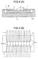
- FIG. 4(A) is a side view showing a state wherein a lead is fixed to the semiconductor chip shown in FIG. 3, and FIG. 4(B) is a plan view showing the state in FIG. 4(A);
- FIG. 5 is a partially sectional view of a conventional resin-sealed semiconductor device;
- FIG. 6 is a partially sectional view showing a problem of the conventional resin-sealed semiconductor device; and
- FIG. 7 is a partially sectional view showing another problem of the resin-sealed semiconductor device.
-
- An embodiment of a resin-sealed semiconductor device according to the present invention will be described below.
- A resin-sealed semiconductor device according to this embodiment, as shown in FIG. 1, is an LOC type semiconductor device comprising a
semiconductor chip 3, alead 1, a leadfixing resin layer 9 and asealing resin layer 2. - The
semiconductor chip 3 is provided with acircuit surface 3a (serving as an upper surface in FIG. 1), and anelectrode 10 is formed on thecircuit surface 3a. Thelead 1 is arranged at a predetermined gap with respect to thesemiconductor chip 3 in such a manner that the distal end of thelead 1 overlaps thesemiconductor chip 3. - A bonding
wire 5 electrically connects the distal end of thelead 1 and theelectrode 10. The leadfixing resin layer 9 is filled between thesemiconductor chip 3 and thelead 1 to fix thelead 1 to thesemiconductor chip 3. The sealingresin layer 2 coated to cover thesemiconductor chip 3 and thelead 1. - The
electrode 10 is formed on thesemiconductor chip 3 such that a plurality ofelectrodes 10 are arranged in two lines at the central portion of thecircuit surface 3a as shown in FIG. 2(A) serving as the side view and FIG. 2(B) serving as the plane view. Thelead 1 connected to theelectrodes 10 is formed such that a plurality ofleads 1 are arranged in correspondence with the number of electrodes. - The gap between the
circuit surface 3a of thesemiconductor chip 3 and the distal end of thelead 1 is about 40 to 100 µm. The leadfixing resin layer 9 is filled between thelead 1 and thecircuit surface 3a over a range from the distal end of thelead 1 to the periphery of thesemiconductor chip 3, i.e., a range in which thelead 1 overlaps thesemiconductor chip 3. - The sealing
resin layer 2 contains filler having a diameter of 50 to 100 µm at a ratio by weight of about 80%, and the remaining 20% is an epoxy-based resin. On the other hand, the leadfixing resin layer 9 also consists of filler and an epoxy-based resin. However, the diameter of the filler is about 1/10 to 1/5 the diameter of the filler contained in the sealingresin layer 2, and is about 1/10 the gap between thelead 1 and thesemiconductor chip 3 at the overlapping portion therebetween. The ratio by weight of the filler contained in the leadfixing resin layer 9 is set to be lower than the ratio by weight of the filler contained in the sealingresin layer 2. More specifically, the leadfixing resin layer 9 contains filler which has a diameter of about 10 µm and whose ratio by weight is about 40%, and the remaining 60% consists of an epoxy-based resin. - As described above, when the
resin layer 9 is used in place of a conventional insulating tape to fix thelead 1, a moisture content in the fixed portion decreases. For this reason, steam generated by heat in practical use can be suppressed, and probability of forming cracks in the sealingresin layer 2 can be reduced. When the filler content is smaller than that in the sealingresin layer 2, probability of clogging filler between thelead 1 and thecircuit surface 3a can be reduced. When the diameter of filler itself is reduced, the filler can be prevented from being clogged. Therefore, stress based on the difference between the coefficient of contraction of the resin and the coefficient of contraction of the filler in solidification of a sealing resin can be prevented from being generated, so that thesemiconductor chip 3 can be prevented from being cracked. - Although the above example explains a case wherein the lead
fixing resin layer 9 contains filler, a material being free from filler can also be used as the leadfixing resin layer 9. - A method of manufacturing a resin-sealed semiconductor device according to the embodiment will be described below. This manufacturing method comprises: the first step of coating the lead
fixing resin layer 9 on thecircuit surface 3a of thesemiconductor chip 3; the second step of fixing the distal ends of the plurality ofleads 1 to thesemiconductor chip 3 with the leadfixing resin layer 9; the third step of bonding the distal ends of theleads 1 and theelectrodes 10 formed on thecircuit surface 3a to each other; and the fourth step of sealing thesemiconductor chip 3 and theleads 1 with thesealing resin layer 2. The respective steps will be sequentially described below. - In the first step, as shown in FIG. 3(A) serving as a side view and FIG. 3(B) serving as a plan view, a
resin 9a for forming the leadfixing resin layer 9 is liquefied, and theliquid resin 9a is supplied from adispenser 11 onto thecircuit surface 3a. Theresin 9a is coated on a position where theleads 1 are fixed, i.e., both the sides of electrode rows in the arrangement direction of theelectrodes 10. The coatedliquid resin 9a initially formes hemisphere shape in the first step. - In the second step, as shown in FIG. 4(A) serving as a side view, the
semiconductor chip 3 is set in arecessed portion 12a formed in aheat block 12, and the plurality ofleads 1 are pressed against theliquid resin 9a from the upper side of FIG. 4(A) to spread theliquid resin 9a. Theheat block 12 is kept at a temperature of 80°C to 100°C, and the leadfixing resin layer 9 serving as a thermosetting resin is solidified for about one minute. The depth of therecessed portion 12a is set such that the level of thecircuit surface 3a is lower than a periphery surrounding surface of the recessedportion 12a by 40 to 100 µm. Thelead 1 is arranged to extend from both the sides of thesemiconductor chip 3 to thecentral electrode 10 as shown in FIG. 4(B) serving as a plan view, and thelead 1 is fixed to thesemiconductor chip 3 with the lead fixingresin layer 9. - In the third step, the
electrode 10 of thesemiconductor chip 3 is electrically connected to the distal end of thelead 1 fixed to thesemiconductor chip 3 in the second step by bonding with thewire 5. And in the fourth step, thesemiconductor chip 3, the distal end of thelead 1, and thewire 5 are sealed with the sealingresin layer 2, and the sealingresin layer 2 is solidified. Thereafter, lead processes such as diver cutting, lead cutting, and lead bending are performed to complete the semiconductor device shown in FIG. 1. - As described above, according to the present invention, when a lead fixing resin layer is used to fix a lead before bonding to a semiconductor chip, a moisture content in the fixed portion decreases. For this reason, steam generated by heat in practical use can be suppressed, and probability of forming cracks in the sealing resin layer can be reduced. In addition, when the diameter of filler contained in the lead fixing resin layer is reduced, probability of clogging the filler between the lead and the semiconductor chip can be reduced. When the diameter of filler itself is reduced, the filler can be prevented from being clogged, and the semiconductor can be prevented from being cracked in solidification of the sealing resin.
- Furthermore, when the filler content in the lead fixing resin layer is made smaller than that in the sealing resin layer, probability of clogging filler between the lead and the circuit surface can be reduced. When a resin being free from filler is used, filler clogging can be canceled. In this manner, stress based on the difference between the coefficient of contraction of the resin and the coefficient of contraction of the filler in solidification of the sealing resin can be prevented from being generated, so that the semiconductor chip can be prevented from being cracked.
Claims (8)
- A resin-sealed semiconductor device comprising:a semiconductor chip having a circuit surface on which a plurality of electrodes are formed;a plurality of leads which are arranged at predetermined gaps with respect to said semiconductor chip in such a manner that distal ends of said leads overlap said semiconductor chip, and which electrically connected to said respective electrodes;a lead fixing resin layer filled between said semiconductor chip and said leads to fix said leads to said semiconductor chip; anda sealing resin layer which is coated to cover the distal ends of said leads and said semiconductor chip which are fixed with said lead fixing resin,
wherein both said lead fixing resin layer and said sealing resin layer contain filler, the diameter of the filler contained in said lead fixing resin layer is smaller than the diameter of filler contained in said sealing resin layer. - A resin-sealed semiconductor device according to claim 1, wherein the diameter of the filler contained in said lead fixing resin layer is about 1/10 to 1/5 the diameter of the filler contained in said sealing resin layer.
- A resin-sealed semiconductor device according to claim 1, wherein the diameter of the filler contained in said lead fixing resin layer is about 1/10 a gap between said leads and said semiconductor chip at an overlapping portion therebetween.
- A resin-sealed semiconductor device according to claim 1, wherein the diameter of the filler contained in said lead fixing resin layer is about 10 µm.
- A resin-sealed semiconductor device according to claim 1, wherein a ratio by weight of the filler contained in said lead fixing resin layer is lower than a ratio by weight of the filler contained in said sealing resin layer.
- A resin-sealed semiconductor device comprising:a semiconductor chip having a circuit surface on which a plurality of electrodes are formed;a plurality of leads which are arranged at predetermined gaps with respect to said semiconductor chip in such a manner that distal ends of said leads overlap said semiconductor chip, and which electrically connected to said respective electrodes;a lead fixing resin layer filled between said semiconductor chip and said leads to fix said leads to said semiconductor chip; anda sealing resin layer which is coated to cover the distal ends of said leads and said semiconductor chip which are fixed with a lead fixing resin,
wherein said lead fixing resin layer is free from filler. - A method of manufacturing a resin-sealed semiconductor device which is formed by sealing a semiconductor chip and leads with a sealing resin layer, comprises:the step of coating a lead fixing resin layer, which contains filler having a diameter smaller than that of filler contained in said sealing resin layer, on a circuit surface of said semiconductor chip;the step of fixing the distal ends of a plurality of leads to said semiconductor chip with said lead fixing resin layer;the step of bonding the distal ends of said leads and electrodes formed on said circuit surface; andthe step of sealing said semiconductor chip and said leads with said sealing resin layer.
- A method of manufacturing a resin-sealed semiconductor device which is formed by sealing a semiconductor chip and leads with a sealing resin layer, comprises:the step of coating a lead fixing resin layer, which is free from filler, on a circuit surface of said semiconductor chip;the step of fixing the distal ends of a plurality of leads to said semiconductor chip with said lead fixing resin layer;the step of bonding the distal ends of said leads and electrodes formed on said circuit surface; andthe step of sealing said semiconductor chip and said leads with said sealing resin layer.
Applications Claiming Priority (3)
| Application Number | Priority Date | Filing Date | Title |
|---|---|---|---|
| JP245808/97 | 1997-09-10 | ||
| JP24580897A JPH1187572A (en) | 1997-09-10 | 1997-09-10 | Resin sealed semiconductor device and production thereof |
| JP24580897 | 1997-09-10 |
Publications (2)
| Publication Number | Publication Date |
|---|---|
| EP0902468A1 true EP0902468A1 (en) | 1999-03-17 |
| EP0902468B1 EP0902468B1 (en) | 2004-10-27 |
Family
ID=17139159
Family Applications (1)
| Application Number | Title | Priority Date | Filing Date |
|---|---|---|---|
| EP19980115366 Expired - Lifetime EP0902468B1 (en) | 1997-09-10 | 1998-08-14 | Resin-sealed semiconductor device and method of manufacturing the device |
Country Status (7)
| Country | Link |
|---|---|
| US (2) | US6274938B1 (en) |
| EP (1) | EP0902468B1 (en) |
| JP (1) | JPH1187572A (en) |
| KR (1) | KR100382965B1 (en) |
| CN (1) | CN100342528C (en) |
| DE (1) | DE69827212T2 (en) |
| TW (1) | TW392316B (en) |
Families Citing this family (5)
| Publication number | Priority date | Publication date | Assignee | Title |
|---|---|---|---|---|
| US6577018B1 (en) * | 2000-08-25 | 2003-06-10 | Micron Technology, Inc. | Integrated circuit device having reduced bow and method for making same |
| SG102637A1 (en) * | 2001-09-10 | 2004-03-26 | Micron Technology Inc | Bow control in an electronic package |
| US7053967B2 (en) * | 2002-05-23 | 2006-05-30 | Planar Systems, Inc. | Light sensitive display |
| CN100378937C (en) * | 2002-05-31 | 2008-04-02 | 威宇科技测试封装有限公司 | Method of wiring on chip by wire soldering technology |
| JP2011023458A (en) * | 2009-07-14 | 2011-02-03 | Toshiba Corp | Semiconductor device and method of manufacturing the same |
Citations (5)
| Publication number | Priority date | Publication date | Assignee | Title |
|---|---|---|---|---|
| US5068712A (en) * | 1988-09-20 | 1991-11-26 | Hitachi, Ltd. | Semiconductor device |
| US5286679A (en) * | 1993-03-18 | 1994-02-15 | Micron Technology, Inc. | Method for attaching a semiconductor die to a leadframe using a patterned adhesive layer |
| US5300459A (en) * | 1989-12-28 | 1994-04-05 | Sanken Electric Co., Ltd. | Method for reducing thermal stress in an encapsulated integrated circuit package |
| EP0651040A1 (en) * | 1993-10-29 | 1995-05-03 | Tomoegawa Paper Co. Ltd. | Liquid adhesive for electronic parts and process for forming insulating adhesive layer using the same |
| WO1997029514A1 (en) * | 1996-02-09 | 1997-08-14 | Mci Computer Gmbh | Semiconductor component |
Family Cites Families (7)
| Publication number | Priority date | Publication date | Assignee | Title |
|---|---|---|---|---|
| US5583375A (en) | 1990-06-11 | 1996-12-10 | Hitachi, Ltd. | Semiconductor device with lead structure within the planar area of the device |
| KR100234824B1 (en) * | 1991-03-20 | 1999-12-15 | 윌리엄 비. 켐플러 | Semiconductor device |
| JP2934357B2 (en) | 1992-10-20 | 1999-08-16 | 富士通株式会社 | Semiconductor device |
| JP2997379B2 (en) * | 1993-03-26 | 2000-01-11 | 京セラ株式会社 | Semiconductor device |
| TW270213B (en) * | 1993-12-08 | 1996-02-11 | Matsushita Electric Ind Co Ltd | |
| JP3350269B2 (en) * | 1995-02-09 | 2002-11-25 | 京セラ株式会社 | Semiconductor device |
| US5759875A (en) * | 1996-10-04 | 1998-06-02 | Micron Technology, Inc. | Reduced filler particle size encapsulant for reduction in die surface damage in LOC packages and method of use |
-
1997
- 1997-09-10 JP JP24580897A patent/JPH1187572A/en active Pending
-
1998
- 1998-08-04 TW TW87112800A patent/TW392316B/en not_active IP Right Cessation
- 1998-08-14 EP EP19980115366 patent/EP0902468B1/en not_active Expired - Lifetime
- 1998-08-14 DE DE1998627212 patent/DE69827212T2/en not_active Expired - Fee Related
- 1998-09-04 KR KR10-1998-0036499A patent/KR100382965B1/en not_active IP Right Cessation
- 1998-09-09 US US09/150,044 patent/US6274938B1/en not_active Expired - Fee Related
- 1998-09-09 CN CNB981191258A patent/CN100342528C/en not_active Expired - Fee Related
-
2001
- 2001-06-07 US US09/875,258 patent/US6541306B2/en not_active Expired - Fee Related
Patent Citations (5)
| Publication number | Priority date | Publication date | Assignee | Title |
|---|---|---|---|---|
| US5068712A (en) * | 1988-09-20 | 1991-11-26 | Hitachi, Ltd. | Semiconductor device |
| US5300459A (en) * | 1989-12-28 | 1994-04-05 | Sanken Electric Co., Ltd. | Method for reducing thermal stress in an encapsulated integrated circuit package |
| US5286679A (en) * | 1993-03-18 | 1994-02-15 | Micron Technology, Inc. | Method for attaching a semiconductor die to a leadframe using a patterned adhesive layer |
| EP0651040A1 (en) * | 1993-10-29 | 1995-05-03 | Tomoegawa Paper Co. Ltd. | Liquid adhesive for electronic parts and process for forming insulating adhesive layer using the same |
| WO1997029514A1 (en) * | 1996-02-09 | 1997-08-14 | Mci Computer Gmbh | Semiconductor component |
Non-Patent Citations (1)
| Title |
|---|
| AMAGAI M ET AL: "DEVELOPMENT OF A TAPELESS LEAD-ON-CHIP (LOC) PACKAGE", PROCEEDINGS OF THE ELECTRONIC COMPONENTS AND TECHNOLOGY CONFERENCE, WASHINGTON, MAY 1 - 4, 1994, no. CONF. 44, 1 May 1994 (1994-05-01), INSTITUTE OF ELECTRICAL AND ELECTRONICS ENGINEERS, pages 506 - 512, XP000479177 * |
Also Published As
| Publication number | Publication date |
|---|---|
| US6274938B1 (en) | 2001-08-14 |
| DE69827212D1 (en) | 2004-12-02 |
| JPH1187572A (en) | 1999-03-30 |
| CN100342528C (en) | 2007-10-10 |
| EP0902468B1 (en) | 2004-10-27 |
| DE69827212T2 (en) | 2005-03-10 |
| TW392316B (en) | 2000-06-01 |
| US6541306B2 (en) | 2003-04-01 |
| KR19990029543A (en) | 1999-04-26 |
| KR100382965B1 (en) | 2003-08-21 |
| US20020000676A1 (en) | 2002-01-03 |
| CN1211074A (en) | 1999-03-17 |
Similar Documents
| Publication | Publication Date | Title |
|---|---|---|
| JP3233535B2 (en) | Semiconductor device and manufacturing method thereof | |
| EP0902468A1 (en) | Resin-sealed semiconductor device and method of manufacturing the device | |
| US6525411B1 (en) | Semiconductor package and method of fabricating the same | |
| US20010038150A1 (en) | Semiconductor device manufactured by package group molding and dicing method | |
| US6265768B1 (en) | Chip scale package | |
| US7023027B2 (en) | Diode package having an anode and a cathode formed on one surface of a diode chip | |
| JP2003124388A (en) | Wafer level chip scale package and method of fabricating the same | |
| JPS5810841A (en) | Resin sealing type semiconductor device | |
| US6838311B2 (en) | Flip chip package and method for forming the same | |
| US6900080B2 (en) | Microelectronic package with reduced underfill and methods for forming such packages | |
| US5043793A (en) | Semiconductor device with stress relief coating at the periphery of the device | |
| JP2005317860A (en) | Resin sealed semiconductor device | |
| JPS59117250A (en) | Semiconductor device | |
| US6949820B2 (en) | Substrate-based chip package | |
| JP3354716B2 (en) | Method for manufacturing semiconductor integrated circuit device | |
| JP2570457B2 (en) | Semiconductor device | |
| JPH0511661B2 (en) | ||
| KR100333383B1 (en) | method of strengthening jointing strength of solder ball of semiconductor package | |
| JPH01135052A (en) | Semiconductor device and manufacture thereof | |
| US6673652B1 (en) | Underfilling method for a flip-chip packaging process | |
| KR100336576B1 (en) | Wafer level package | |
| JP2826432B2 (en) | Semiconductor device | |
| JP2680969B2 (en) | Semiconductor memory device | |
| KR200202059Y1 (en) | adhesive for bonding chip in fabrication of vari able chip-size applicable package | |
| JPH02285649A (en) | Semiconductor device |
Legal Events
| Date | Code | Title | Description |
|---|---|---|---|
| PUAI | Public reference made under article 153(3) epc to a published international application that has entered the european phase |
Free format text: ORIGINAL CODE: 0009012 |
|
| AK | Designated contracting states |
Kind code of ref document: A1 Designated state(s): DE FR GB NL |
|
| AX | Request for extension of the european patent |
Free format text: AL;LT;LV;MK;RO;SI |
|
| 17P | Request for examination filed |
Effective date: 19990803 |
|
| AKX | Designation fees paid |
Free format text: DE FR GB NL |
|
| 17Q | First examination report despatched |
Effective date: 20030401 |
|
| GRAP | Despatch of communication of intention to grant a patent |
Free format text: ORIGINAL CODE: EPIDOSNIGR1 |
|
| GRAS | Grant fee paid |
Free format text: ORIGINAL CODE: EPIDOSNIGR3 |
|
| RIN1 | Information on inventor provided before grant (corrected) |
Inventor name: ANZAI, NORITAKA Inventor name: OHUCHI, SHINJI |
|
| GRAA | (expected) grant |
Free format text: ORIGINAL CODE: 0009210 |
|
| AK | Designated contracting states |
Kind code of ref document: B1 Designated state(s): DE FR GB NL |
|
| REG | Reference to a national code |
Ref country code: GB Ref legal event code: FG4D |
|
| REF | Corresponds to: |
Ref document number: 69827212 Country of ref document: DE Date of ref document: 20041202 Kind code of ref document: P |
|
| PGFP | Annual fee paid to national office [announced via postgrant information from national office to epo] |
Ref country code: GB Payment date: 20050802 Year of fee payment: 8 |
|
| PGFP | Annual fee paid to national office [announced via postgrant information from national office to epo] |
Ref country code: NL Payment date: 20050818 Year of fee payment: 8 |
|
| PGFP | Annual fee paid to national office [announced via postgrant information from national office to epo] |
Ref country code: FR Payment date: 20050819 Year of fee payment: 8 |
|
| PLBE | No opposition filed within time limit |
Free format text: ORIGINAL CODE: 0009261 |
|
| STAA | Information on the status of an ep patent application or granted ep patent |
Free format text: STATUS: NO OPPOSITION FILED WITHIN TIME LIMIT |
|
| ET | Fr: translation filed | ||
| 26N | No opposition filed |
Effective date: 20050728 |
|
| PGFP | Annual fee paid to national office [announced via postgrant information from national office to epo] |
Ref country code: DE Payment date: 20051026 Year of fee payment: 8 |
|
| PG25 | Lapsed in a contracting state [announced via postgrant information from national office to epo] |
Ref country code: NL Free format text: LAPSE BECAUSE OF NON-PAYMENT OF DUE FEES Effective date: 20070301 Ref country code: DE Free format text: LAPSE BECAUSE OF NON-PAYMENT OF DUE FEES Effective date: 20070301 |
|
| GBPC | Gb: european patent ceased through non-payment of renewal fee |
Effective date: 20060814 |
|
| NLV4 | Nl: lapsed or anulled due to non-payment of the annual fee |
Effective date: 20070301 |
|
| REG | Reference to a national code |
Ref country code: FR Ref legal event code: ST Effective date: 20070430 |
|
| PG25 | Lapsed in a contracting state [announced via postgrant information from national office to epo] |
Ref country code: GB Free format text: LAPSE BECAUSE OF NON-PAYMENT OF DUE FEES Effective date: 20060814 |
|
| PG25 | Lapsed in a contracting state [announced via postgrant information from national office to epo] |
Ref country code: FR Free format text: LAPSE BECAUSE OF NON-PAYMENT OF DUE FEES Effective date: 20060831 |