EP0894330B1 - Anzeigevorrichtung - Google Patents
Anzeigevorrichtung Download PDFInfo
- Publication number
- EP0894330B1 EP0894330B1 EP98900025A EP98900025A EP0894330B1 EP 0894330 B1 EP0894330 B1 EP 0894330B1 EP 98900025 A EP98900025 A EP 98900025A EP 98900025 A EP98900025 A EP 98900025A EP 0894330 B1 EP0894330 B1 EP 0894330B1
- Authority
- EP
- European Patent Office
- Prior art keywords
- display device
- envelope
- selection structure
- connection elements
- electrodes
- Prior art date
- Legal status (The legal status is an assumption and is not a legal conclusion. Google has not performed a legal analysis and makes no representation as to the accuracy of the status listed.)
- Expired - Lifetime
Links
- 239000000463 material Substances 0.000 claims abstract description 39
- 229910000639 Spring steel Inorganic materials 0.000 claims abstract description 4
- 230000003647 oxidation Effects 0.000 claims description 5
- 238000007254 oxidation reaction Methods 0.000 claims description 5
- 238000007669 thermal treatment Methods 0.000 claims description 2
- 239000011521 glass Substances 0.000 description 10
- 238000007789 sealing Methods 0.000 description 9
- 238000004519 manufacturing process Methods 0.000 description 6
- PXHVJJICTQNCMI-UHFFFAOYSA-N Nickel Chemical compound [Ni] PXHVJJICTQNCMI-UHFFFAOYSA-N 0.000 description 5
- 238000010276 construction Methods 0.000 description 5
- 239000000037 vitreous enamel Substances 0.000 description 5
- 229910000640 Fe alloy Inorganic materials 0.000 description 3
- XEEYBQQBJWHFJM-UHFFFAOYSA-N Iron Chemical compound [Fe] XEEYBQQBJWHFJM-UHFFFAOYSA-N 0.000 description 2
- 229910045601 alloy Inorganic materials 0.000 description 2
- 239000000956 alloy Substances 0.000 description 2
- 239000005388 borosilicate glass Substances 0.000 description 2
- 239000011651 chromium Substances 0.000 description 2
- 239000011248 coating agent Substances 0.000 description 2
- 238000000576 coating method Methods 0.000 description 2
- PCHJSUWPFVWCPO-UHFFFAOYSA-N gold Chemical compound [Au] PCHJSUWPFVWCPO-UHFFFAOYSA-N 0.000 description 2
- 239000010931 gold Substances 0.000 description 2
- 229910052737 gold Inorganic materials 0.000 description 2
- 229910052751 metal Inorganic materials 0.000 description 2
- 239000002184 metal Substances 0.000 description 2
- 238000000034 method Methods 0.000 description 2
- 230000001590 oxidative effect Effects 0.000 description 2
- VYZAMTAEIAYCRO-UHFFFAOYSA-N Chromium Chemical compound [Cr] VYZAMTAEIAYCRO-UHFFFAOYSA-N 0.000 description 1
- 229910000531 Co alloy Inorganic materials 0.000 description 1
- 229910000831 Steel Inorganic materials 0.000 description 1
- KGWWEXORQXHJJQ-UHFFFAOYSA-N [Fe].[Co].[Ni] Chemical compound [Fe].[Co].[Ni] KGWWEXORQXHJJQ-UHFFFAOYSA-N 0.000 description 1
- 230000002411 adverse Effects 0.000 description 1
- YCLAMANSVUJYPT-UHFFFAOYSA-L aluminum chloride hydroxide hydrate Chemical compound O.[OH-].[Al+3].[Cl-] YCLAMANSVUJYPT-UHFFFAOYSA-L 0.000 description 1
- 229910052785 arsenic Inorganic materials 0.000 description 1
- 229910052804 chromium Inorganic materials 0.000 description 1
- BIJOYKCOMBZXAE-UHFFFAOYSA-N chromium iron nickel Chemical compound [Cr].[Fe].[Ni] BIJOYKCOMBZXAE-UHFFFAOYSA-N 0.000 description 1
- 210000003298 dental enamel Anatomy 0.000 description 1
- 238000006073 displacement reaction Methods 0.000 description 1
- 238000010348 incorporation Methods 0.000 description 1
- 229910052742 iron Inorganic materials 0.000 description 1
- 239000004973 liquid crystal related substance Substances 0.000 description 1
- 239000011572 manganese Substances 0.000 description 1
- WPBNNNQJVZRUHP-UHFFFAOYSA-L manganese(2+);methyl n-[[2-(methoxycarbonylcarbamothioylamino)phenyl]carbamothioyl]carbamate;n-[2-(sulfidocarbothioylamino)ethyl]carbamodithioate Chemical compound [Mn+2].[S-]C(=S)NCCNC([S-])=S.COC(=O)NC(=S)NC1=CC=CC=C1NC(=S)NC(=O)OC WPBNNNQJVZRUHP-UHFFFAOYSA-L 0.000 description 1
- 150000002739 metals Chemical class 0.000 description 1
- 229910052759 nickel Inorganic materials 0.000 description 1
- 229910000623 nickel–chromium alloy Inorganic materials 0.000 description 1
- 238000005192 partition Methods 0.000 description 1
- 230000001681 protective effect Effects 0.000 description 1
- 239000005361 soda-lime glass Substances 0.000 description 1
- 125000006850 spacer group Chemical group 0.000 description 1
- 239000010959 steel Substances 0.000 description 1
Images

Classifications
-
- H—ELECTRICITY
- H01—ELECTRIC ELEMENTS
- H01J—ELECTRIC DISCHARGE TUBES OR DISCHARGE LAMPS
- H01J31/00—Cathode ray tubes; Electron beam tubes
- H01J31/08—Cathode ray tubes; Electron beam tubes having a screen on or from which an image or pattern is formed, picked up, converted, or stored
- H01J31/10—Image or pattern display tubes, i.e. having electrical input and optical output; Flying-spot tubes for scanning purposes
- H01J31/12—Image or pattern display tubes, i.e. having electrical input and optical output; Flying-spot tubes for scanning purposes with luminescent screen
- H01J31/123—Flat display tubes
- H01J31/125—Flat display tubes provided with control means permitting the electron beam to reach selected parts of the screen, e.g. digital selection
- H01J31/126—Flat display tubes provided with control means permitting the electron beam to reach selected parts of the screen, e.g. digital selection using line sources
-
- H—ELECTRICITY
- H01—ELECTRIC ELEMENTS
- H01J—ELECTRIC DISCHARGE TUBES OR DISCHARGE LAMPS
- H01J29/00—Details of cathode-ray tubes or of electron-beam tubes of the types covered by group H01J31/00
- H01J29/92—Means forming part of the tube for the purpose of providing electrical connection to it
-
- H—ELECTRICITY
- H01—ELECTRIC ELEMENTS
- H01R—ELECTRICALLY-CONDUCTIVE CONNECTIONS; STRUCTURAL ASSOCIATIONS OF A PLURALITY OF MUTUALLY-INSULATED ELECTRICAL CONNECTING ELEMENTS; COUPLING DEVICES; CURRENT COLLECTORS
- H01R12/00—Structural associations of a plurality of mutually-insulated electrical connecting elements, specially adapted for printed circuits, e.g. printed circuit boards [PCB], flat or ribbon cables, or like generally planar structures, e.g. terminal strips, terminal blocks; Coupling devices specially adapted for printed circuits, flat or ribbon cables, or like generally planar structures; Terminals specially adapted for contact with, or insertion into, printed circuits, flat or ribbon cables, or like generally planar structures
- H01R12/50—Fixed connections
- H01R12/51—Fixed connections for rigid printed circuits or like structures
- H01R12/52—Fixed connections for rigid printed circuits or like structures connecting to other rigid printed circuits or like structures
-
- H—ELECTRICITY
- H01—ELECTRIC ELEMENTS
- H01J—ELECTRIC DISCHARGE TUBES OR DISCHARGE LAMPS
- H01J2329/00—Electron emission display panels, e.g. field emission display panels
- H01J2329/92—Means forming part of the display panel for the purpose of providing electrical connection to it
Definitions
- the invention relates to a display device having a vacuum-tight envelope comprising a transparent front wall which is provided with a display screen having a pattern of luminescent pixels, which display device comprises an internal selection structure which is provided with holes and with a plurality of electrodes for addressing desired pixels.
- Display devices for displaying monochromatic or color images comprise, inter alia, (flat) cathode ray tubes (CRTs), plasma display panels (PDPs) and plasma-addressed liquid-crystal display devices (PALC displays).
- CTRs cathode ray tubes
- PDPs plasma display panels
- PLC displays plasma-addressed liquid-crystal display devices
- a display device is known from United States Patent US 5,313,136 (PHN 12.927).
- the display device (of the thin type) described in said document comprises a vacuum envelope having a transparent front wall an inner surface of which is provided with a display screen having a pattern of luminescent pixels, and said vacuum envelope further comprises a rear wall (which is connected to the front wall by side walls and/or partitions) which extends parallel to the front wall.
- the known display device comprises at least an electron source for generating electrons and addressing means for guiding said electrons to the display screen.
- the addressing means comprise a selection structure, which is composed of a stack of flat plates which are provided with coaxial apertures and on which a plurality of electrodes are provided for addressing the electrons. As soon as the electrons have passed through the selection structure, they are accelerated so as to provide the electrons with sufficient energy to excite the luminescent pixels, so that a high luminance is achieved.
- a type of plasma display panels comprises, in a vacuum envelope, a selection structure provided with holes and with row electrodes and column electrodes, which selection structure is situated between a rear wall provided with a plasma cathode and a front wall provided with a display screen having a pattern of luminescent pixels.
- a gas discharge is maintained between the plasma cathode and a (series of) row electrode(s), which serve(s) as the anode.
- a number of electrons from the gas discharge, which arrive at the anode pass through the holes of the selection structure at a location where a row electrode and a column electrode cross each other.
- the current through the selection structure is determined by the voltage applied across the column electrode corresponding to the relevant row electrode. As soon as the electrons have passed through the selection structure, they are accelerated so as to provide the electrons with sufficient energy to excite the luminescent pixels, so that a high luminance is achieved.
- a plasma is generated which plasma produces UV-light to address the relevant luminescent pixels by means of the selection structure.
- a disadvantage of the known display device is that rejects occur during the manufacture thereof, which is undesirable.
- connection elements which each comprise a springy end portion, which contacts an electrode on the selection structure, and which connection elements further comprise a feed-through portion to make an electric connection, through a wall of the envelope, between the electrodes and a voltage source situated outside the envelope.
- the invention is based on the recognition that it is desirable to make a construction for contacting the electrodes on the selection structure, the (electric) connection with the electrodes on the selection structure being made in the interior of the vacuum-tight envelope.
- the electric connections to the electrodes on the selection structure are made outside the vacuum-tight envelope, the selection structure being passed to the outside through a (side) wall of the vacuum-tight envelope. This applies, in particular, to selection structures composed of a number of plates.
- connection elements which each comprise a springy end portion which electrically contacts an electrode on the selection structure, which connection elements further comprise a feed-through portion for passing the connection elements through a (side) wall of the envelope.
- the selection structure does not have to be fed through (a side wall of) the vacuum-tight envelope, the selection structure itself does not form part of the (wall of the) vacuum-tight envelope.
- the alignment of (the plates of) the selection structure relative to the pixels which alignment must meet high accuracy requirements due to the presence of a plurality of holes for selectively passing the electrons or for selectively generating a plasma (pdp)
- pdp a plasma
- the selection structure is not situated partly inside the envelope and partly outside the envelope, a difference in pressure distribution on (the plates of) the selection structure is precluded in this manner.
- a bend in (a plate of) the selection structure may, in addition, give rise to a poor adhesion between an electrode and (the plate of) the selection structure, which may lead to rejects. Particularly in the case of large display devices (having a picture diameter, for example, of 100 cm) with large-scale selection structures, this increases the risk of rejects.
- the risk of rejects during the manufacture of the display device is reduced.
- An additional advantage is that the service life of the display device is increased by incorporating the (critical) (connection) elements in the interior of the display device. Oxidation of the electrodes and of the springy end portions is precluded by contacting the electrodes of the selection structure inside the vacuum-tight envelope.
- An embodiment of the display device in accordance with the invention is characterized in that the springy end portion comprises a material which retains its springiness up to a temperature of at least 450 °C.
- the springy end portion comprises a material which retains its springiness up to a temperature of at least 450 °C.
- the springy end portion is preferably made of a material whose limit of elasticity remains so high, after a temperature treatment up to approximately 450 °C, that the remaining springiness is sufficient to preserve the electric contact.
- the springy end portion is made of a material whose modulus of elasticity is above 20.10 10 Pa.
- a material which can particularly suitably be used for the springy end portion is a so-called spring steel, for example an alloy comprising iron, chromium, nickel and manganese, such as an iron alloy comprising 16-18 % by weight of Cr, 6-9 % by weight of Ni and ⁇ 2 % by weight of Mn (preferably ⁇ 1.5 % by weight of Si).
- the feed-through portion comprises a material whose expansion is adapted to that of the material of the envelope.
- the coefficient of expansion of the feed-through portion of the connection element should be adapted to the coefficient of expansion of the (glass) frit or the vitreous enamel.
- the material used for the feed-through portion is a so-called expansion alloy.
- the material of the envelope influences the choice of the material used for the feed-through portion.
- an iron-nickel-cobalt alloy (a so-called "fernico-steel" for fusion-sealing of glass) can suitably be used as the material for the feed-through portion.
- a material which can very suitably be used for fusion-sealing of glass is a material having a linear coefficient of expansion in the range from 5.8 to 6.2 ⁇ 10 -6 K -1 , for example an iron alloy comprising 28 % by weight of Ni and 18 % by weight of Co.
- an iron-nickel-chromium alloy can suitably be used as the material for the feed-through portion.
- a particularly suitable material for fusion-sealing of glass is a material having a linear coefficient of expansion in the range from 9 to 10 ⁇ 10 -6 K -1 , for example an iron alloy comprising 47 % by weight of Ni and 5 % by weight of Co.
- connection elements comprise, outside the envelope, a further end portion of a material which reduces oxidation of the further end portion during a thermal treatment at temperatures up to at least 450 °C under atmospheric conditions.
- a temperature increase occurs in the display device.
- the further end portion makes a satisfactory electric contact if said further end portion is connected to the voltage source.
- said further end portion is made of the same material as the feed-through portion.
- the material used for said further end portion may also comprise (other) poorly oxidizing or refined metals.
- the further end portion may also be provided with an oxidation-reducing material, for example a gold layer.
- the feed-through portion and/or the further end portion is/are surrounded by a protective gas when the temperature increases during sealing the display device in a vacuum-tight manner.
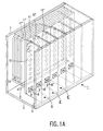
- Fig. 1A is a very schematic, perspective view, partly cut away, of an example of a construction of a display device 1 (flat CRT), which is provided with a selection structure in accordance with the invention.
- the selection structure comprises a stack of flat plates.
- the invention is important, in particular, for this type of flat display devices.
- the display device comprises a front wall (window) 3 and an opposing rear wall 4, which extends parallel to said front wall 3.
- This electron source 5 comprises, for example, a cathode arrangement comprising one or more line cathodes or a large number of separate electrodes.
- a number of electron-propagation means, which cooperate with the electron source 5, are arranged next to said electron sources, which electron-propagation means are formed by ducts 6, 6', 6" etc., which are separated from the electron-propagation means by walls 12, 12', 12" etc., which extend at right angles to the rear wall 4 so as to form the ducts of a so-called duct structure.
- the electron-propagation means cooperate, via a so-called cathode plate having (entrance) apertures 8, 8', 8", etc., and electrodes 9, 9', 9", etc., with the electron source 5 and extend substantially parallel to the front wall.
- the apertures 8, 8', 8", etc. are rectangular.
- the apertures 8, 8', 8", etc. are square, round, oval or of any other shape.
- the electron source 5 is arranged in the extension of (i.e. below) the duct structure.
- a selection structure, which closes the ducts 6, 6', 6", etc., is provided with holes 7, 7', 7", etc., to selectively pass the electrons.
- the selection structure 10 comprises a stack of a number of (flat) plates 11, 11 ' , 11", etc., provided with holes 7, 7', 7", etc.
- the plates 11, 11', 11", etc., of the selection structure 10 have been displaced relative to each other and provided with electrodes (not shown in Fig. 1A) to address desired pixels.
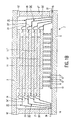
- Fig. 1B very schematically shows, in cross-section, a plan view of the display device 1 shown in Fig. 1A.
- Side walls 2'; 2" connect the front wall 3 to the rear wall 4 by means of so-called glass frits or vitreous enamels 15, 15'; 16, 16', so that a vacuum-tight envelope is formed.
- the side walls 2'; 2" may alternatively form part of the rear wall 4 or the front wall 3.
- the walls 12, 12', 12" etc. separate the ducts 6, 6', 6” etc., from each other, which ducts form the electron-propagation means (the electron source is not shown in Fig. 1B).
- connection elements 21, 21'; 22, 22' in accordance with the invention, which electrically connect the electrodes on the plates 11, 11', 11", etc., of the selection structure to a voltage source (not shown in Fig. 1B) which is situated outside the envelope.
- the connection elements 21.21'; 22, 22' comprise springy end portions 23, 23'; 24, 24', which contact an electrode on the selection structure.
- the connection elements 21, 21'; 22, 22' further comprise feed-through portions 25, 25'; 26, 26', which bring about an electric connection between the selection structure and the voltage source via a glass frit or a vitreous enamel 15; 16.
- connection elements 21, 21'; 22, 22' comprise further end portions 27; 28 for making electric connections to the voltage source.
- these further end portions 27; 28 may also comprise a further springy end portion.
- parts of said connection elements may be made of an oxidation-reducing material (for example a poorly oxidizing or refined metal) or be provided with an oxidation-reducing coating, for example a gold layer. It is alternatively possible to surround the display device with a protective-gas atmosphere.
- the selection structure comprises a plurality of stacked, flat plates 11, 11', 11" etc., which are provided with electrodes. These plates are displaced relative to each other in such a manner that they do not overlap at locations where the springy end portions 23, 23'; 24, 24' of the connection elements 21, 21'; 22, 22' contact the electrodes on the plates of the selection structure.
- the advantage of such a displacement is that the plates of the selection structure have the same dimensions, which simplifies the manufacture of the selection structure.
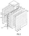
- Fig. 2 is a very schematic, perspective view, partly cut away, of a part of an alternative construction of a display device.
- This display device of the thin type is a so-called plasma display panel (PDP).
- the plasma display panel 41 comprises, in a vacuum envelope, a selection structure 47; 47' provided with holes (not shown in Fig. 2) and with row electrodes and column electrodes 51, 51'; 52, 52', which selection structure is arranged between a rear wall 44 provided with one or more plasma cathodes 45, 45' and a front wall 43 provided with a display screen having a pattern of luminescent pixels 46, 46', 46", etc.
- the selection structure comprises a stack of two plates 47, 47'.
- a gas discharge is maintained between the plasma cathode 45, 45' and a (series of) row electrode(s) 51, 51', which serve(s) as the anode.
- a number of electrons from the gas discharge, which arrive at the anode, pass through the holes in the (plates of the) selection structure 47; 47' at the location where a row electrode and a column electrode cross each other.
- the current through the selection structure 47; 47' is determined by the voltage applied across the column electrodes 52, 52' corresponding to the relevant row electrode.
- connection elements in accordance with the invention connect the electrodes 51, 51'; 52, 52' on the plates of the selection structure 47; 47' to a voltage source (not shown in Fig. 2) which is situated outside the envelope.
- the plasma generates UV-light which exits the holes of the selection structure 47; 47', which UV-light addresses the relevant luminescent pixels 46, 46', 46", etc., of the display screen on the frontwall 43 of the plasma display panel.
- Fig. 3 is a schematic, perspective view of a part of a selection structure 67 provided with connection elements 71, 72 in accordance with the invention.
- the connection elements 71; 72 electrically connect the electrodes on the plates 60; 60" of the selection structure 67 to a voltage source (not shown in Fig. 3) outside the envelope. Plates 60' are contacted on the other side of the selection structure (not shown in Fig. 3).
- the connection elements 71; 72 comprise springy end portions 73; 74 which contact an electrode 61; 62 on the selection structure 67.
- connection elements 71; 72 further comprise feed-through portions 75; 76 which electrically connect the selection structure 67 to the voltage source through a side wall (not shown in Fig. 3) of the envelope.
- the springy end portions 73, 74 and the feed-through portions 75, 76 are connected to each other, for example by means of a welded joint 80. This is the case, notably, if the materials of the springy end portions 73, 74 and of the feed-through portions 75, 76 are different.
- the requirements to be met by the materials of the connection elements 71; 72 generally are different.
- connection elements 71; 72 comprise further end portions 77; 78 for making electric connections to the voltage source, which further end portions 77; 78 may be made of or provided with an oxidation-reducing material or coating.
- the selection structure 67 comprises a plurality of stacked flat plates 60, 60', 60", etc., which are provided with electrodes 61; 62. These plates are displaced relative to each other in such a manner that they do not overlap at locations where the springy end portions 73; 74 of the connection elements 71; 72 contact the electrodes on the plates of the selection structure 67.
- connection elements During mounting of the connection elements, a plurality of connection elements are interconnected via a strip 85.
- a strip 85 is situated on the side of the further end portions 77; 78 of the connection elements 71; 72. After mounting of the connection elements 71; 72, this strip 85 is removed.
- the invention relates to a display device comprising a vacuum-tight envelope having a transparent front wall provided with a display screen and a rear wall which extends parallel to said front wall.
- the display device comprises an internal selection structure which is provided with holes and with a plurality of electrodes for addressing desired pixels on the display screen.
- the display device is provided with connection elements which each comprise a springy end portion, which contacts an electrode on the selection structure, and which connection elements further comprise a feed-through portion for making an electric connection, through a wall of the envelope, between the electrodes and a voltage source situated outside the envelope.
- the springy end portion comprises a material which retains its springiness up to temperatures of at least 450 °C, for example a spring steel, and the material of the feed-through portion is adapted to the expansion of the material of the envelope.
- the plates of the selection structure are displaced relative to each other in such a manner that the plates do not overlap at locations where the springy end portions of the connection elements contact the electrodes. During mounting, the connection elements are coupled to each other via a strip.
Landscapes
- Cathode-Ray Tubes And Fluorescent Screens For Display (AREA)
- Vessels, Lead-In Wires, Accessory Apparatuses For Cathode-Ray Tubes (AREA)
- Gas-Filled Discharge Tubes (AREA)
- Devices For Indicating Variable Information By Combining Individual Elements (AREA)
Claims (7)
- Wiedergabeanordnung (1) mit einer vakuumdichten Hülle mit einer transparenten Vorderwand (3), die mit einem Wiedergabeschirm versehen ist, der ein Muster leuchtender Pixel aufweist, wobei diese Wiedergabeanordnung (1) eine interne Selektionsstruktur (10, G7) aulweist, die mit Löchern (7) versehen ist sowie mit einer Anzahl Elektroden zum Adressieren gewünschter Pixel , dadurch gekennzeichnet, dass die Wiedergabeanordnung (1) mit Verbindungselementen (21, 21', 22, 22') versehen ist, die je einen federnden Endteil (23, 23'; 24, 24') aufweisen, der eine Elektrode auf der Selektionsstruktur (10, 67) kontaktiert und wobei diese Verbindungselemente weiterhin einen Durchrührungsteil (25, 25'; 26, 26') aufweisen um eine elektrische Verbindung zu machen, und zwar durch eine Wand (2'; 2") der Hülle, zwischen den Elektroden und einer Spannungsquelle, die sich außerhalb der Hülle befindet.
- Wiedergabeanordnung nach Anspruch 1, dadurch gekennzeichnet, dass der federnde Endteil (23, 23'; 24, 24') ein Material umfasst, das bis zu Temperaturen von wenigstens 450°C seine Federkraft beibehält.
- Wiedergabeanordnung nach Anspruch 2, dadurch gekennzeichnet, dass das Material des federnden Endteils (23, 23'; 24, 24') einen Federstahl enthält.
- Wiedergabeanordnung nach Anspruch 1 oder 2, dadurch gekennzeichnet, dass der Durchführungsteil (25, 25'; 26, 26') ein Material aufweist, dessen Ausdehnung an die des Materials der Hülle angepasst ist.
- Wiedergabeanordnung nach einem der vorstehenden Ansprüche, dadurch gekennzeichnet, dass die Verbindungselemente (21, 21'; 22, 22') außerhalb der Hülle einen weiteren Endteil (27; 28) aus einem Material aufweisen, das Oxidation des weiteren Endteils (27; 28) während einer thermischen Behandlung bis zu wenigstens 450°C unter atmosphärischen Umständen reduziert.
- Wiedergabeanordnung nach Anspruch 1 oder 2, dadurch gekennzeichnet, dass die Selektionsstruktur (67) eine Anzahl flacher Platten (60, 60', 60") aufweist, die mit Elektroden (61, 62) versehen sind, wobei diese Platten (60, 60', 60") gegenüber einander derart verschoben sind, dass die Platten (60, 60', 60") an Stellen, wo die federnden Endteile (73, 74) der Verbindungselemente (71, 72) die Elektroden (61, 62) kontaktieren, nicht überlappen.
- Wiedergabeanordnung nach Anspruch 6, dadurch gekennzeichnet, dass die flachen Platten (60, 60', 60") an wechselnden Seiten mit Verbindungselementen (71, 72) versehen sind.
Priority Applications (1)
| Application Number | Priority Date | Filing Date | Title |
|---|---|---|---|
| EP98900025A EP0894330B1 (de) | 1997-01-20 | 1998-01-12 | Anzeigevorrichtung |
Applications Claiming Priority (4)
| Application Number | Priority Date | Filing Date | Title |
|---|---|---|---|
| EP97200159 | 1997-01-20 | ||
| EP97200159 | 1997-01-20 | ||
| EP98900025A EP0894330B1 (de) | 1997-01-20 | 1998-01-12 | Anzeigevorrichtung |
| PCT/IB1998/000028 WO1998032151A1 (en) | 1997-01-20 | 1998-01-12 | Display device, a connection element for use in said display device, and a strip provided with such connection elements |
Publications (2)
| Publication Number | Publication Date |
|---|---|
| EP0894330A1 EP0894330A1 (de) | 1999-02-03 |
| EP0894330B1 true EP0894330B1 (de) | 2003-06-04 |
Family
ID=8227944
Family Applications (1)
| Application Number | Title | Priority Date | Filing Date |
|---|---|---|---|
| EP98900025A Expired - Lifetime EP0894330B1 (de) | 1997-01-20 | 1998-01-12 | Anzeigevorrichtung |
Country Status (5)
| Country | Link |
|---|---|
| US (1) | US6008572A (de) |
| EP (1) | EP0894330B1 (de) |
| JP (1) | JP2000508826A (de) |
| DE (1) | DE69815220T2 (de) |
| WO (1) | WO1998032151A1 (de) |
Families Citing this family (1)
| Publication number | Priority date | Publication date | Assignee | Title |
|---|---|---|---|---|
| JP2000067741A (ja) * | 1998-08-26 | 2000-03-03 | Futaba Corp | 扁平型真空容器の電極構造 |
Family Cites Families (4)
| Publication number | Priority date | Publication date | Assignee | Title |
|---|---|---|---|---|
| NL9000060A (nl) * | 1989-06-01 | 1991-01-02 | Philips Nv | Beeldweergeefinrichting van het dunne type. |
| US5557296A (en) * | 1989-06-01 | 1996-09-17 | U.S. Philips Corporation | Flat-panel type picture display device with insulating electron-propagation ducts |
| ES2093355T3 (es) * | 1992-06-12 | 1996-12-16 | Philips Electronics Nv | Dispositivo de presentacion de imagenes de tipo panel plano con conductos aislantes de propagacion de electrones. |
| JPH07254504A (ja) * | 1994-12-20 | 1995-10-03 | Hokuriku Electric Ind Co Ltd | 電子部品及び高電圧用電子部品 |
-
1998
- 1998-01-12 DE DE69815220T patent/DE69815220T2/de not_active Expired - Fee Related
- 1998-01-12 JP JP10529170A patent/JP2000508826A/ja active Pending
- 1998-01-12 EP EP98900025A patent/EP0894330B1/de not_active Expired - Lifetime
- 1998-01-12 WO PCT/IB1998/000028 patent/WO1998032151A1/en active IP Right Grant
- 1998-01-16 US US09/008,341 patent/US6008572A/en not_active Expired - Fee Related
Also Published As
| Publication number | Publication date |
|---|---|
| US6008572A (en) | 1999-12-28 |
| DE69815220D1 (de) | 2003-07-10 |
| DE69815220T2 (de) | 2004-04-08 |
| JP2000508826A (ja) | 2000-07-11 |
| EP0894330A1 (de) | 1999-02-03 |
| WO1998032151A1 (en) | 1998-07-23 |
Similar Documents
| Publication | Publication Date | Title |
|---|---|---|
| EP0405262A1 (de) | Anzeigevorrichtung mit flachem Bildschirm | |
| US6998769B2 (en) | Image displaying apparatus having a potential regulating electrode, an anode, and a spacing member, for suppressing undesired discharge | |
| US7095169B2 (en) | Flat panel display device | |
| KR20040038780A (ko) | 용기의 제조방법 및 전자선장치의 제조방법 | |
| JP2006019247A (ja) | 画像表示装置 | |
| JP4481891B2 (ja) | 画像表示装置 | |
| KR100661009B1 (ko) | 화상형성장치와 이것을 구비한 텔레비젼 장치 | |
| EP0894330B1 (de) | Anzeigevorrichtung | |
| KR20070014840A (ko) | 저저항 스페이서를 이용한 전자방출표시장치 | |
| US7839071B2 (en) | Vacuum container and method for manufacturing the same, and image display apparatus and method for manufacturing the same | |
| US20070222362A1 (en) | Image display apparatus | |
| JP2000315468A (ja) | 画像形成装置 | |
| US20070120460A1 (en) | Image display device | |
| JP4481892B2 (ja) | 画像表示装置 | |
| JP2002367540A (ja) | 画像表示装置 | |
| KR20040101628A (ko) | 평판형 칼라 디스플레이 장치 | |
| JP4036417B2 (ja) | 画像形成装置 | |
| JP2566155B2 (ja) | 平板型画像表示装置 | |
| WO2005048288A1 (ja) | 画像表示装置 | |
| JPH03208240A (ja) | 平板型陰極線表示装置 | |
| JPH02177239A (ja) | 平板型crt | |
| JP4089786B2 (ja) | 画像表示装置 | |
| JP2002197998A (ja) | 電子線装置及び画像形成装置及び電子線装置の製造方法 | |
| JP2002075254A (ja) | 画像形成装置 | |
| EP1876629A1 (de) | Plasmaanzeigetafel und verfahren zu ihrer herstellung |
Legal Events
| Date | Code | Title | Description |
|---|---|---|---|
| PUAI | Public reference made under article 153(3) epc to a published international application that has entered the european phase |
Free format text: ORIGINAL CODE: 0009012 |
|
| AK | Designated contracting states |
Kind code of ref document: A1 Designated state(s): DE FR GB |
|
| 17P | Request for examination filed |
Effective date: 19990125 |
|
| 17Q | First examination report despatched |
Effective date: 20020424 |
|
| GRAH | Despatch of communication of intention to grant a patent |
Free format text: ORIGINAL CODE: EPIDOS IGRA |
|
| RTI1 | Title (correction) |
Free format text: DISPLAY DEVICE |
|
| RTI1 | Title (correction) |
Free format text: DISPLAY DEVICE |
|
| GRAH | Despatch of communication of intention to grant a patent |
Free format text: ORIGINAL CODE: EPIDOS IGRA |
|
| GRAA | (expected) grant |
Free format text: ORIGINAL CODE: 0009210 |
|
| AK | Designated contracting states |
Designated state(s): DE FR GB |
|
| REG | Reference to a national code |
Ref country code: GB Ref legal event code: FG4D |
|
| REG | Reference to a national code |
Ref country code: GB Ref legal event code: 746 Effective date: 20030610 |
|
| REF | Corresponds to: |
Ref document number: 69815220 Country of ref document: DE Date of ref document: 20030710 Kind code of ref document: P |
|
| PG25 | Lapsed in a contracting state [announced via postgrant information from national office to epo] |
Ref country code: GB Free format text: LAPSE BECAUSE OF NON-PAYMENT OF DUE FEES Effective date: 20040112 |
|
| ET | Fr: translation filed | ||
| PLBE | No opposition filed within time limit |
Free format text: ORIGINAL CODE: 0009261 |
|
| STAA | Information on the status of an ep patent application or granted ep patent |
Free format text: STATUS: NO OPPOSITION FILED WITHIN TIME LIMIT |
|
| REG | Reference to a national code |
Ref country code: FR Ref legal event code: D6 |
|
| 26N | No opposition filed |
Effective date: 20040305 |
|
| PG25 | Lapsed in a contracting state [announced via postgrant information from national office to epo] |
Ref country code: DE Free format text: LAPSE BECAUSE OF NON-PAYMENT OF DUE FEES Effective date: 20040803 |
|
| GBPC | Gb: european patent ceased through non-payment of renewal fee |
Effective date: 20040112 |
|
| PG25 | Lapsed in a contracting state [announced via postgrant information from national office to epo] |
Ref country code: FR Free format text: LAPSE BECAUSE OF NON-PAYMENT OF DUE FEES Effective date: 20040930 |
|
| REG | Reference to a national code |
Ref country code: FR Ref legal event code: ST |