EP0890296B1 - Apparatuses for controlling phase difference in plasma processing systems - Google Patents
Apparatuses for controlling phase difference in plasma processing systems Download PDFInfo
- Publication number
- EP0890296B1 EP0890296B1 EP97916806A EP97916806A EP0890296B1 EP 0890296 B1 EP0890296 B1 EP 0890296B1 EP 97916806 A EP97916806 A EP 97916806A EP 97916806 A EP97916806 A EP 97916806A EP 0890296 B1 EP0890296 B1 EP 0890296B1
- Authority
- EP
- European Patent Office
- Prior art keywords
- signal
- phase
- circuit
- peak
- power source
- Prior art date
- Legal status (The legal status is an assumption and is not a legal conclusion. Google has not performed a legal analysis and makes no representation as to the accuracy of the status listed.)
- Expired - Lifetime
Links
- 238000012545 processing Methods 0.000 title claims abstract description 33
- 238000005259 measurement Methods 0.000 claims description 26
- 239000004065 semiconductor Substances 0.000 claims description 6
- 230000001939 inductive effect Effects 0.000 claims description 4
- 238000004519 manufacturing process Methods 0.000 claims description 4
- 238000000034 method Methods 0.000 abstract description 32
- 230000010363 phase shift Effects 0.000 description 49
- 229920002120 photoresistant polymer Polymers 0.000 description 33
- 230000008569 process Effects 0.000 description 24
- 230000000694 effects Effects 0.000 description 23
- 238000005530 etching Methods 0.000 description 8
- XAGFODPZIPBFFR-UHFFFAOYSA-N aluminium Chemical compound [Al] XAGFODPZIPBFFR-UHFFFAOYSA-N 0.000 description 6
- 229910052782 aluminium Inorganic materials 0.000 description 6
- 230000003628 erosive effect Effects 0.000 description 4
- 239000000463 material Substances 0.000 description 4
- 230000003287 optical effect Effects 0.000 description 4
- 238000011160 research Methods 0.000 description 4
- 239000003990 capacitor Substances 0.000 description 3
- 238000005229 chemical vapour deposition Methods 0.000 description 2
- 238000007796 conventional method Methods 0.000 description 2
- 239000000112 cooling gas Substances 0.000 description 2
- 230000008878 coupling Effects 0.000 description 2
- 238000010168 coupling process Methods 0.000 description 2
- 238000005859 coupling reaction Methods 0.000 description 2
- 239000013078 crystal Substances 0.000 description 2
- 238000013461 design Methods 0.000 description 2
- 238000002474 experimental method Methods 0.000 description 2
- 239000010408 film Substances 0.000 description 2
- 239000001307 helium Substances 0.000 description 2
- 229910052734 helium Inorganic materials 0.000 description 2
- SWQJXJOGLNCZEY-UHFFFAOYSA-N helium atom Chemical compound [He] SWQJXJOGLNCZEY-UHFFFAOYSA-N 0.000 description 2
- 150000002500 ions Chemical class 0.000 description 2
- 238000001465 metallisation Methods 0.000 description 2
- 230000003647 oxidation Effects 0.000 description 2
- 238000007254 oxidation reaction Methods 0.000 description 2
- 230000001681 protective effect Effects 0.000 description 2
- 239000000523 sample Substances 0.000 description 2
- 239000000126 substance Substances 0.000 description 2
- 229910015844 BCl3 Inorganic materials 0.000 description 1
- ATJFFYVFTNAWJD-UHFFFAOYSA-N Tin Chemical compound [Sn] ATJFFYVFTNAWJD-UHFFFAOYSA-N 0.000 description 1
- RTAQQCXQSZGOHL-UHFFFAOYSA-N Titanium Chemical compound [Ti] RTAQQCXQSZGOHL-UHFFFAOYSA-N 0.000 description 1
- -1 aluminum-silicon-copper Chemical compound 0.000 description 1
- 238000002048 anodisation reaction Methods 0.000 description 1
- 230000003667 anti-reflective effect Effects 0.000 description 1
- 230000004888 barrier function Effects 0.000 description 1
- 239000004020 conductor Substances 0.000 description 1
- 239000013256 coordination polymer Substances 0.000 description 1
- 230000003247 decreasing effect Effects 0.000 description 1
- 238000000151 deposition Methods 0.000 description 1
- 230000008021 deposition Effects 0.000 description 1
- 238000001514 detection method Methods 0.000 description 1
- 230000003116 impacting effect Effects 0.000 description 1
- 230000000977 initiatory effect Effects 0.000 description 1
- 238000012986 modification Methods 0.000 description 1
- 230000004048 modification Effects 0.000 description 1
- 238000012544 monitoring process Methods 0.000 description 1
- 238000002161 passivation Methods 0.000 description 1
- 238000000206 photolithography Methods 0.000 description 1
- 238000005268 plasma chemical vapour deposition Methods 0.000 description 1
- 229910021420 polycrystalline silicon Inorganic materials 0.000 description 1
- 229920005591 polysilicon Polymers 0.000 description 1
- 239000010453 quartz Substances 0.000 description 1
- VYPSYNLAJGMNEJ-UHFFFAOYSA-N silicon dioxide Inorganic materials O=[Si]=O VYPSYNLAJGMNEJ-UHFFFAOYSA-N 0.000 description 1
- 238000004544 sputter deposition Methods 0.000 description 1
- 230000000087 stabilizing effect Effects 0.000 description 1
- 239000010409 thin film Substances 0.000 description 1
- 239000010936 titanium Substances 0.000 description 1
- 229910052719 titanium Inorganic materials 0.000 description 1
- 238000012546 transfer Methods 0.000 description 1
- FAQYAMRNWDIXMY-UHFFFAOYSA-N trichloroborane Chemical compound ClB(Cl)Cl FAQYAMRNWDIXMY-UHFFFAOYSA-N 0.000 description 1
Images

Classifications
-
- H—ELECTRICITY
- H01—ELECTRIC ELEMENTS
- H01J—ELECTRIC DISCHARGE TUBES OR DISCHARGE LAMPS
- H01J37/00—Discharge tubes with provision for introducing objects or material to be exposed to the discharge, e.g. for the purpose of examination or processing thereof
- H01J37/32—Gas-filled discharge tubes
- H01J37/32009—Arrangements for generation of plasma specially adapted for examination or treatment of objects, e.g. plasma sources
- H01J37/32082—Radio frequency generated discharge
- H01J37/321—Radio frequency generated discharge the radio frequency energy being inductively coupled to the plasma
-
- H—ELECTRICITY
- H01—ELECTRIC ELEMENTS
- H01J—ELECTRIC DISCHARGE TUBES OR DISCHARGE LAMPS
- H01J37/00—Discharge tubes with provision for introducing objects or material to be exposed to the discharge, e.g. for the purpose of examination or processing thereof
- H01J37/32—Gas-filled discharge tubes
- H01J37/32009—Arrangements for generation of plasma specially adapted for examination or treatment of objects, e.g. plasma sources
- H01J37/32082—Radio frequency generated discharge
- H01J37/32137—Radio frequency generated discharge controlling of the discharge by modulation of energy
- H01J37/32155—Frequency modulation
- H01J37/32165—Plural frequencies
-
- H—ELECTRICITY
- H01—ELECTRIC ELEMENTS
- H01J—ELECTRIC DISCHARGE TUBES OR DISCHARGE LAMPS
- H01J37/00—Discharge tubes with provision for introducing objects or material to be exposed to the discharge, e.g. for the purpose of examination or processing thereof
- H01J37/32—Gas-filled discharge tubes
- H01J37/32009—Arrangements for generation of plasma specially adapted for examination or treatment of objects, e.g. plasma sources
- H01J37/32082—Radio frequency generated discharge
- H01J37/32174—Circuits specially adapted for controlling the RF discharge
- H01J37/32183—Matching circuits
-
- H—ELECTRICITY
- H01—ELECTRIC ELEMENTS
- H01J—ELECTRIC DISCHARGE TUBES OR DISCHARGE LAMPS
- H01J37/00—Discharge tubes with provision for introducing objects or material to be exposed to the discharge, e.g. for the purpose of examination or processing thereof
- H01J37/32—Gas-filled discharge tubes
- H01J37/32917—Plasma diagnostics
- H01J37/32935—Monitoring and controlling tubes by information coming from the object and/or discharge
- H01J37/32963—End-point detection
-
- H—ELECTRICITY
- H01—ELECTRIC ELEMENTS
- H01J—ELECTRIC DISCHARGE TUBES OR DISCHARGE LAMPS
- H01J37/00—Discharge tubes with provision for introducing objects or material to be exposed to the discharge, e.g. for the purpose of examination or processing thereof
- H01J37/32—Gas-filled discharge tubes
- H01J37/32917—Plasma diagnostics
- H01J37/32935—Monitoring and controlling tubes by information coming from the object and/or discharge
- H01J37/32972—Spectral analysis
-
- H—ELECTRICITY
- H01—ELECTRIC ELEMENTS
- H01J—ELECTRIC DISCHARGE TUBES OR DISCHARGE LAMPS
- H01J37/00—Discharge tubes with provision for introducing objects or material to be exposed to the discharge, e.g. for the purpose of examination or processing thereof
- H01J37/32—Gas-filled discharge tubes
- H01J37/32917—Plasma diagnostics
- H01J37/3299—Feedback systems
-
- H—ELECTRICITY
- H05—ELECTRIC TECHNIQUES NOT OTHERWISE PROVIDED FOR
- H05H—PLASMA TECHNIQUE; PRODUCTION OF ACCELERATED ELECTRICALLY-CHARGED PARTICLES OR OF NEUTRONS; PRODUCTION OR ACCELERATION OF NEUTRAL MOLECULAR OR ATOMIC BEAMS
- H05H1/00—Generating plasma; Handling plasma
- H05H1/24—Generating plasma
- H05H1/46—Generating plasma using applied electromagnetic fields, e.g. high frequency or microwave energy
Definitions
- the present invention relates to apparatuses for inducing plasma in plasma enhanced processing systems, which are typically used in semiconductor fabrication. More specifically, the invention relates to apparatuses for controlling the phase shift between generators in plasma processing systems to achieve desired process results.
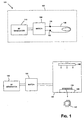
- Fig. 1 shows a chemical etch reactor 100, representing a plasma generating system which utilizes an inductive coil for plasma generation.
- Reactor 100 includes coil system 102 and chamber 124.
- Coil system 102 includes a coil element 106, which is excited by a radio frequency generator 110.
- Coil element 106 is coupled to a matching circuit 108 for matching the impedance of coil element 106 to that of radio frequency generator 110.
- the matching of the impedances permits radio frequency generator 110 to efficiently deliver power to coil element 106.
- the chamber wall of chamber 124 is typically grounded.
- the ground path may be provided through the lower electrode, e.g., a chuck 128 of Fig. 1, when the plasma is confined.
- shower head 126 Within chamber 124, there typically exists a shower head 126.
- shower head 126 is shown disposed above a chuck 128 and wafer 134, which is supported by chuck 128.
- Chuck 128 acts as a second electrode and is preferably biased by its independent radio frequency circuit 120 via a matching network 122.
- coil element 106 and match 108 are typically disposed proximate to chamber 124 while RF generator 110 may be placed in any reasonable location.
- shower head 126 represents the apparatus for dispensing etchant or deposition materials onto wafer 134.
- shower head 126 preferably includes a plurality of holes for releasing gaseous source materials (typically around the periphery edge of shower head 126) into the RF-induced plasma region between itself and wafer 134 during operation.
- gaseous source materials typically around the periphery edge of shower head 1266
- shower head 126 is made of quartz although it may also be made of other suitable materials and may be left either electrically floating or grounded.
- generators 110 and 120 are typically driven at a given RF frequency. To ensure that both generators deliver power at the same frequency, they may be frequency-locked in a master-and-slave configuration. For example, lower (bias) generator 120 may be designated the master, and the frequency of the upper (coil) generator 110 may slaved to that of master generator 120 (or vice versa). Frequency locking may be achieved by any conventional technique, including, e.g., disabling the frequency-generating crystal in the slave generator and employing the frequency-generating crystal in the master generator to drive both the master and slave generators.
- phase difference may arise due to factors internal to the generators themselves or due to system parameters such as the difference in the lengths of the cables that couple the generators to their respective electrodes. It is discovered that the phase difference may give rise to undesirable or unexpected process and electrical characteristics, which may lead to uncertain consequences on the process results.
- US-5,116482 describes a film forming system using capacitive plasma generation for sputtering thin films.
- the system includes a first master RF power supply connected to a top capacitive electrode by a matching box.
- a second slave RF power supply is connected to a bottom capacitive electrode by a second matching box.
- a first monitor sensor detects the voltage of the top electrode and a second monitor sensor detects the voltage of the bottom electrode.
- the outputs of the monitor sensors are passed to a phase adjusting device which is also supplied with an externally set signal.
- the phase adjusting device generates a phase shifting signal to controls the slave RF power supply to have a phase difference with respect to the master power supply corresponding to the phase difference set by the externally set signal.
- a plasma processing system for generating plasma for use in semiconductor fabrication, said plasma processing system having a first radio frequency (RF) power source for outputting a first RF signal to a first electrode and a second RF power source for outputting a second RF signal to a second electrode, said second RF power source being coupled to said first RF power source as a slave RF power source in a master-and-slave configuration, said plasma processing system comprising a control circuit, including: a first sensor circuit coupled to said first electrode for detecting a phase of said first RF signal; a first matching circuit connected between the first RF power source and the first electrode; a second sensor circuit coupled to said second electrode for detecting a phase of said second RF signal; a second matching circuit connected between the second RF power source and the second electrode; a mixer circuit coupled to said first sensor circuit and said second sensor circuit for detecting a phase difference between said first RF signal and said second RF signal and for outputting a first signal representing said phase difference; a phase difference
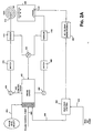
- Fig. 2A is a schematic illustrating, according to the present invention, the overall control circuit for controlling the phase difference between two frequency-locked generators of a plasma processing system.
- RF generators 402 and 404 are arranged in a master-and-slave configuration with RF generator 402 acting as the reference generator. Power to the plasma in a plasma processing chamber 406 are delivered by these two RF generators 402 and 404 through match circuits 408 and 410, respectively.
- the chuck RF generator e.g., RF generator 402
- the master generator e.g., the master generator in Fig. 2A
- the invention applies equally well when the RF generator associated with the upper electrode, e.g., RF generator 404, is designated the master.
- the upper electrode 412 is shown having an Archimedes spiral coil in Fig. 2A, other suitable electrodes may well be employed to generate plasma within the plasma processing chamber.
- One end of the coil may be isolated from ground, e.g., through a transformer, or grounded.
- a sensor 414 is coupled to one end of coil 412. Sensor 414 is disposed between coil 412 and match network 410 to avoid the effects of the tuning networks that are used for impedance matching. Likewise, a sensor 416 is coupled between chuck electrode 418 and match circuit 408 to ascertain the phase of the RF signal supplied to chuck electrode 418.
- phase servo circuit 422 which may be implemented by an error amplifier or any number of known phase servo circuit designs, compares the feedback signal from mixer circuit 420 with a phase control set point signal 424 to output a control signal 430 to the slave generator, e.g., RF generator 404 in Fig. 2A. Responsive to control signal 430, the slave generator then modifies its phase, thereby causing the phase difference between the phases of the RF signals detected by sensors 414 and 416 to substantially match the value specified by phase control set point signal 424.
- phase control set point value 424 may represent a predefined value to facilitate system matching, i.e., to ensure that the difference between the phases of the RF signals supplied to the upper electrode and lower electrode is substantially the same from machine to machine.
- the inventive technique of feedback control to ensure that the phase difference conforms to a predefined value is referred to herein as passive control of the phase difference.
- passive control of the phase difference When the phase difference is passively controlled, it is possible to ensure that the phase difference between the phases of the RF signals will stay substantially constant across different systems irrespective of system parameters, e.g., the placement of the RF generators relative to the plasma processing chamber.
- phase control set point value 424 may represent a user-variable value for actively controlling the phase difference between the phases of the RF signals to achieve desired process results.
- the inventive technique of actively modifying the phase difference to achieve specific desired process results is referred to herein as active control of the phase difference.
- a user may specify that the RF signal supplied to the upper electrode lead the RF signal supplied to the lower electrode by 180 to maximize aluminum-to-photoresist selectivity during an aluminum etch step (the effect of the phase difference on the aluminum-to-photoresist selectivity is illustrated in a subsequent Fig. 9 herein).
- the user may specify that the RF power supplies deliver their power in phase to maximize the etch rate during an oxide etch step (Fig. 6A).
- Other examples are readily apparent to those skilled in the art upon reviewing the figures and the disclosure herein.
- either the chuck's RF peak-to-peak a.c. voltage or the wafer's d.c. voltage may be used as a feedback signal to facilitate control of either of those two values by changing the phase difference.
- an a.c./d.c. bias measurement circuit 440 represents, for ease of illustration, the circuit for measuring either the chuck's RF peak-to-peak a.c. voltage or the wafer's d.c. voltage (depending on the embodiment).
- a.c./d.c. bias measurement circuit 440 may represent a d.c. bias measurement circuit.
- a.c./d.c. bias measurement circuit 440 may represent either a d.c. bias measurement circuit or one that measures the chuck's RF peak-to-peak a.c. voltage.
- the chuck's RF peak-to-peak a.c. voltage may be measured using a voltage probe or any other conventional technique.
- the wafer's d.c. voltage may be sensed by, for example, employing a probe inside chamber 406 to sense the state of the plasma within chamber 406, or by inferring it from the chuck's RF peak-to-peak a.c. voltage itself.
- a method of inferring the wafer's d.c. bias from the chuck's RF peak-to-peak a.c. voltage reference may be made to the commonly-assigned, co-pending patent applications entitled “Dynamic Feedback Electrostatic Chuck,” (U.S. patent no. 5,812,361) and “Voltage Controller for Electrostatic Chuck of Vacuum Plasma Processors" by Neil Benjamin, Seyed Jafar Jafarian-Tehrani, and Max Artussi (U.S. patent no. 5,708,250), both filed on even date.
- Peak bias control circuit 442 represents the circuit for comparing the signal output by a.c./d.c. bias measurement circuit 440 with a user-input bias set point signal 444 and for outputting an error signal 446. Responsive to this error signal, phase servo circuit 422 then modifies control signal 430, thereby modifying the phase difference between the RF signals supplied by the two RF generators and indirectly modifying either chuck's RF peak-to-peak a.c. voltage or the wafer's d.c. bias voltage (depending on the implementation of ac/dc bias measurement circuit 440) until it matches the bias set point signal 444.
- the signal output by a.c./d.c. bias measurement circuit 440 may be monitored by an appropriate logic circuit to allow the user to, for example, determine the phase difference that results in a specific value of chuck's RF peak-to-peak a.c. voltage (or wafer's d.c. bias voltage).
- the phase of the slave generator may be modified while monitoring the value output by a.c./d.c. bias measurement circuit 440 to ascertain the phase difference value that results in, e.g., the highest or lowest chuck's RF peak-to-peak a.c. voltage (or wafer's d.c. bias voltage).
- phase servo circuit 422 Since these specific values of the chuck's RF peak-to-peak a.c. voltage (or the wafer's d.c. bias voltage) are directly related to specific process characteristics, the user may then employ the ascertained phase difference as an input into phase servo circuit 422 to ensure that the desired process results can be obtained more reliably and consistently.
- the inventive control circuit does not have to include all the components shown in Fig. 2A. It includes essentially of sensors 414 and 416, mixer circuit 420, two electrodes 412, 418, matching circuits 408, 410, and phase servo circuit 422. With these circuit blocks, the detection of the phase difference between the RF signals supplied by the RF power supplies and the modification of that phase difference are facilitated. If it is desired to also modify the phase difference to achieve a specific RF peak-to-peak a.c. voltage set point or a specific wafer d.c. voltage set point, the control circuit may include a.c./d.c. bias measurement circuit 440 and peak bias control circuit 442 of Fig. 2A.
- Match circuits 408 and 410 may be implemented by any number of conventional match circuits.
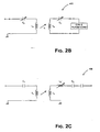
- Fig. 2B shows an implementation of upper TCP match circuit 410 that has been found to be suitable.
- capacitor Cs resonates the inductance of the TCP coil.
- Capacitor C P transforms the load impedance to match the source impedance of the RF power source, which is typically about 50 ⁇ .
- Inductors L P and L S are primary and secondary inductances of the match transformer. The values of these inductances L P and L S depend on the coil size and the coupling factor between the coil and the plasma.
- One version of match circuit 410 known by its part number 853-031685-001, is available from the aforementioned Lam Research Corp.
- Fig. 2C illustrates an implementation of lower TCP match circuit 408.
- variable inductor Ls' is employed to resonate the load.
- Variable coupling factor K transforms the load to the proper impedance to maximize power delivery by the RF generator.
- match circuit 408 known by its part number 853-015130-002, is available from the aforementioned Lam Research Corp.
- Fig. 2D illustrates a d.c. bias measurement circuit that is suitable for implementing a.c./d.c. bias measurement circuit 440.
- the chuck's RF signal is sensed through a plurality of resistors 460, which provides a high impedance to ground to limit amount of RF current drawn.
- resistors 460 there are five resistors 460 in series to reduce the capacitive division effect of the d.c. bias measurement circuit.
- Resistors 470 and 472 form a resistor network for scaling down the signal received through the plurality of resistors 460.
- Capacitor 474 is coupled in parallel with resistors 470 and 472 to supply a d.c.
- the effects of the phase shift on process characteristics are investigated to determine whether changes to the phase shift impact certain critical process parameters such as the RF peak-to-peak voltage on the lower electrode, the wafer d.c. bias, etch rates, aluminum-to-photoresist selectivity, and others.
- certain critical process parameters such as the RF peak-to-peak voltage on the lower electrode, the wafer d.c. bias, etch rates, aluminum-to-photoresist selectivity, and others.
- the disclosed invention may be practiced in any plasma etch systems to etch, among others, the metallization layer, the oxide layer, or the polysilicon layer.
- the invention may also be practiced, as can be appreciated by those skilled in the art, in plasma CVD systems to control film characteristics such as density and/or stress, or in any plasma processing systems, which may be employed for annodization, oxidation, or the like.
- plasma CVD systems to control film characteristics such as density and/or stress
- any plasma processing systems which may be employed for annodization, oxidation, or the like.
- two frequency-locked Advanced Energy 1,250 Watt 13.56 MHz RF generators are configured in a master-and-slave configuration to provide power to a TCP 9600TM etching system, which is available from Lam Research Corporation of Fremont, California.
- the lower (bias) generator is employed as the master to the upper (TCP) slave generator (although the invention applies equally well when the upper generator serves as the master).
- an ENI VL400 phase shift controller by ENI which is a division of Astec America Inc. of Rochester, New York, was coupled to both generators to keep the lower (bias) generator fixed and to phase shift the upper (TCP) generator relative to the lower generator.
- a patterned wafer from SEMATECH of Austin, Texas was exposed to a partial etch.
- This SEMATECH wafer comprises the following layers: photoresist layer, TiN arc (anti-reflective) layer, metallization layer comprising aluminum-silicon-copper, barrier layer comprising titanium, and oxide layer.
- oxide a wafer having thereon patterned thermal oxide is employed.
- the process settings for the experiments related to Figs. 3-13 are approximately as follows: Power to top electrode (watts) 400 Power to bottom electrode (watts) 100 Reactor chamber pressure (Pa) 0.67 (5 m Torr) Cl 2 flow rate (m 3 s -1 ) 1 ⁇ 10 -6 (62 sccm) BCl 3 flow rate (m 3 s -1 ) 3 ⁇ 10 -7 (18 sccm) Wafer Temperature (°C) 50 Helium cooling gas (Pa) 1,600 (12 Torr)
- phase shift settings were employed: - 90° (i.e., the top generator lags the bottom generator by 90°), 0° (i.e., they are in phase), 90° (i.e., the top generator leads the bottom generator by 90°), and 180° (i.e., they are opposite in phase).
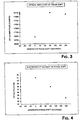
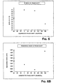
- Fig. 3 is a graph illustrating, in accordance with one aspect of the present invention, the effect of the phase shift on the optical amplitude of the 261 nm plasma emission, which is employed to determine the endpoint for the aluminum etch.
- the mean value of the 261 nm signal when the generators are running in phase was observed to be low relative to the mean value of the same signal when the generators were running at - 90°, 90°, and 180° out of phase respectively.
- the lower mean value of the optical signal suggests that relatively less intense plasma is present when the power is delivered by the two generators in phase.
- Fig. 4 is a graph illustrating, in accordance with one aspect of the present invention, the effect of the phase shift on the lower (bias) electrode RF peak-to-peak voltage.
- Fig. 3 indicates that changes in phase shift indeed result in changes in the lower electrode RF peak-to-peak voltage in the range from about 34 to 41 volts, with the lower electrode RF peak-to-peak voltage attaining its maximum when the generators are in phase, as shown in Fig. 4.
- the phase shift e.g., using the circuit of Fig. 2A or another suitable control circuit, the lower electrode RF peak-to-peak voltage may be controlled, leading to improved process results.
- the d.c. bias of Fig. 5 tracked the lower electrode peak-to-peak voltage and varies from about - 39 volts to - 26 volts as the phase difference was shifted from 0° to 180°, as shown in Fig. 5.
- the changes in the d.c. bias voltage indicates that the plasma characteristics are significantly impacted by the phase shift.
- the d.c. bias voltage is directly linked to the process occurring on the wafer since when the d.c. bias is higher, the etching ions will likely impact the wafer with a higher energy to result in a higher etch rate and a more anisotropic etch.
- etching for semiconductor devices is a precise balancing of chemical and physical processes, and physical etching is tied directly to the difference between the plasma potential and the d.c. potential on the wafer, the bias needs to be under tight control, not only to ensure that repeatable process results can be achieved, but also to harness the phase shift to enhance process results, e.g., maximize or minimize the etch rates or the anisotropic etch quality.
- the etch results suggest that desirable process characteristics may be achieved by controlling, either passively or actively, the phase difference between the RF signals supplied by the RF power supplies.
- the wafer d.c. bias or the lower electrode RF peak-to-peak voltage since there is a correspondence between the wafer d.c. bias or the lower electrode RF peak-to-peak voltage and the phase shift, it is possible, as mentioned earlier in connection with Fig. 2A, to employ either the wafer d.c. bias or the lower electrode peak-to-peak voltage as a feedback signal to a phase control circuit in order to passively or actively control the phase difference, i.e., to either maintain a desired phase difference value across different plasma processing systems or to actively control the phase difference to enhance process results.
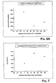
- Fig. 6A is a graph illustrating, in accordance with one aspect of the present invention, the effect of the phase shift on the oxide etch rate.
- the oxide etch rate is approximately 1,600 angstroms per minute.
- the oxide etch rate is up to about 1,750 angstroms per minute.
- the oxide etch rate when the top power supply leads the bottom power supply by 90° and 180° is significantly lower, at about 1,400 and 1,500 angstroms (10 -10 m) per minute respectively.
- etch rate difference of up to about 300 angstroms per minute may be obtained when the phase shift changes from 0° to 90°.
- Fig. 6B is a graph illustrating, in accordance with one aspect of the present invention, the effect of the phase shift on the remaining oxide thickness.
- the oxide thickness is at its lowest when the phase difference is about 90° and is high when the phase difference is either 0° or 180°. Consequently, changes to the phase difference do indeed impact the remaining oxide thickness, and further point to the advantages that may be achieved when the phase difference is controlled.
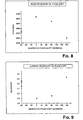
- Fig. 7 is a graph illustrating, in accordance with one aspect of the present invention, the effect of the phase shift on the aluminum-to-oxide selectivity.
- the selectivity varies significantly responsive to the phase shift, having values of about 5.6, 5.0, 6.5, and 6.0 for a phase shift value of about - 90°, 0°, 90°, and 180°, respectively.
- a high wafer d.c. bias (as seen in Fig. 5) and low selectivity.
- the wafer d.c. bias is at its highest (in Fig. 5) while the aluminum-to-oxide selectivity is at its lowest (in Fig. 7).
- a high d.c. bias may increase the energy of the impacting ions, thereby decreasing the aluminum-to-oxide selectivity.
- Fig. 8 is a graph illustrating, in accordance with one aspect of the present invention, the effect of the phase shift on the photoresist etch rate. Again, changes in the phase shift appear to significantly impact the etch rate of the photoresist with an etch rate of as high as over about 3,000 angstroms per minute when the power supplies are in phase, and about 2,600 angstroms per minute when the power supplies are about 180° out of phase.
- Fig. 9 illustrates, in accordance with one aspect of the present invention, that changing the phase shift also significantly impacts the aluminum-to-photoresist selectivity.
- the lowest aluminum-to-photoresist selectivity is obtained when the power supplies are delivering power to the plasma in phase (0° phase shift).
- the maximum selectivity, as illustrated in Fig. 9, is achieved when the power supplies are delivering power at about 180° out of phase. This has several important implications. As manufacturers move toward smaller devices, a high aluminum-to-photoresist selectivity is valuable. This is because as the lines become thinner, the photoresist layer must be thinner.
- a thinner photoresist layer requires a higher aluminum-to-photoresist selectivity so that the protective photoresist layer does not get inadvertently etched away, resulting in damage to the underlying features.
- Fig. 9 suggests that increased aluminum-to-photoresist selectivity can be achieved by changing the phase shift between the RF power supplies.
- the highest etch rate and lowest selectivities are obtained when the power supplies are in phase. It appears that the aluminum-to-photoresist selectivity can be improved when the power supplies are delivering power to the plasma out of phase. For example, the highest aluminum-to-oxide selectivity occurs when the power supplies are about 90° out of phase (Fig. 7), and the highest aluminum-to-photoresist selectivity occurs when the power supplies are about 180° out of phase (Fig. 9).
- Figs. 8 and 9 also suggest that the slowest photoresist etch rate and the highest aluminum-to-photoresist selectivity are obtained when the power supplies are delivering power to the plasma at about 180° out of phase. At about 180°, it can be expected that more of the photoresist will remain, i.e., less of the photoresist layer will get etched away, resulting in better protection of the underlying features.
- the ability to adjust the hardware to improve the ability of a given photoresist layer to protect the underlying features is particularly valuable as devices are scaled smaller and smaller.
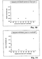
- Figs. 10 and 11 remaining photoresist on 0.8 ⁇ m feature is measured, after etching with a recipe commonly used to etch through the aluminum layer in semiconductor manufacturing, at the center of the wafer (Fig. 10), and at the edge of the wafer (Fig. 11). As shown in Figs. 10 and 11, maximum remaining photoresist thickness measurements occur when the power supplies deliver their power at about 180° phase shift. Note that the remaining photoresist thickness measurements are maximized and minimized at the same phase shifts, i.e., at 180° phase shift and about 90° phase shift respectively, in both Fig. 10 and Fig. 11.
- Figs. 12 and 13 illustrate the effect of the phase shift on the critical dimension (CD) at the center of the wafer and the edge of the wafer respectively.
- the critical dimension (CD) represents the post-etch measurement of the line width.
- Maximum critical dimension measurements were obtained when the generators were in the high bias, in-phase condition, when photoresist erosion was at a maximum.
- a high amount of photoresist erosion passivates the sidewall to a greater degree to protect the aluminum against erosion, resulting in more protection for the lines and a greater CD measurement.
- Minimum critical dimension measurements occur at both the wafer center and the wafer edge when the generators were running at a phase shift of about 180° and, as shown in Fig. 8, the photoresist etch rate is at its minimum.
- Fig. 14 shows, the steps involved in an etch method, in which the phase difference between the RF signals supplied by the RF power supplies are controlled, either actively or passively, to achieve the desired process results.
- the wafer is prepared for etching in a conventional pre-etch step.
- the pre-etch steps may include, for example, conventional photolithography steps, clamping the wafer on the chuck, stabilizing the pressure within the plasma processing chamber, and introducing helium cooling gas to the wafer backside to facilitate heat transfer between the wafer and the chuck, among others.
- step 502 the phase difference between the RF signals provided by the RF power supplies is controlled, e.g., using the circuit of Fig. 2A.
- the control may be passive (i.e., to ensure that the phase difference does not vary from a predefined value), or active (i.e., actively control the phase difference to match a user-specified phase difference value).
- step 504 at least a portion of one layer of the wafer layer stack is etched while controlling the phase difference. Note that although this step 504 occurs after step 502, control of the phase difference preferably continues during etching. Further, step 504 may be initiated either before, contemporaneous with, or after the initiation of step 502.
- the wafer may undergo additional processing steps to fabricate the desired components as well as post-etch processing steps that are conventional in nature. Thereafter, the finished wafer may be cut into dies, which may then be made into IC chips. The resulting IC chip, e.g., IC chips 140 of Fig. 1, may then be incorporated in an electronic device, e.g., any of the of well known commercial or consumer electronic devices, including digital computers.
- an electronic device e.g., any of the of well known commercial or consumer electronic devices, including digital computers.
Landscapes
- Physics & Mathematics (AREA)
- Engineering & Computer Science (AREA)
- Plasma & Fusion (AREA)
- Chemical & Material Sciences (AREA)
- Analytical Chemistry (AREA)
- Spectroscopy & Molecular Physics (AREA)
- Electromagnetism (AREA)
- Plasma Technology (AREA)
- Drying Of Semiconductors (AREA)
- Chemical Vapour Deposition (AREA)
- Discharge Heating (AREA)
- Investigating, Analyzing Materials By Fluorescence Or Luminescence (AREA)
Applications Claiming Priority (3)
| Application Number | Priority Date | Filing Date | Title |
|---|---|---|---|
| US08/642,172 US5824606A (en) | 1996-03-29 | 1996-03-29 | Methods and apparatuses for controlling phase difference in plasma processing systems |
| US642172 | 1996-03-29 | ||
| PCT/US1997/004271 WO1997037518A1 (en) | 1996-03-29 | 1997-03-19 | Methods and apparatuses for controlling phase difference in plasma processing systems |
Publications (2)
| Publication Number | Publication Date |
|---|---|
| EP0890296A1 EP0890296A1 (en) | 1999-01-13 |
| EP0890296B1 true EP0890296B1 (en) | 2005-11-23 |
Family
ID=24575500
Family Applications (1)
| Application Number | Title | Priority Date | Filing Date |
|---|---|---|---|
| EP97916806A Expired - Lifetime EP0890296B1 (en) | 1996-03-29 | 1997-03-19 | Apparatuses for controlling phase difference in plasma processing systems |
Country Status (9)
Families Citing this family (38)
| Publication number | Priority date | Publication date | Assignee | Title |
|---|---|---|---|---|
| JP3220394B2 (ja) * | 1996-09-27 | 2001-10-22 | 東京エレクトロン株式会社 | プラズマ処理装置 |
| US6214162B1 (en) | 1996-09-27 | 2001-04-10 | Tokyo Electron Limited | Plasma processing apparatus |
| JPH10214822A (ja) * | 1997-01-30 | 1998-08-11 | Nec Corp | プラズマエッチング装置およびエッチング方法 |
| JPH10335096A (ja) * | 1997-06-03 | 1998-12-18 | Hitachi Ltd | プラズマ処理装置 |
| DE19737244A1 (de) * | 1997-08-27 | 1999-03-04 | Harald Tobies | Vorrichtung und Verfahren zur Regelung der Phasenlage von Hochfrequenzelektroden bei Plasmaprozessen |
| WO1999014699A1 (en) * | 1997-09-17 | 1999-03-25 | Tokyo Electron Limited | System and method for monitoring and controlling gas plasma processes |
| US6348679B1 (en) * | 1998-03-17 | 2002-02-19 | Ameritherm, Inc. | RF active compositions for use in adhesion, bonding and coating |
| US6483871B1 (en) * | 1998-12-28 | 2002-11-19 | Nortel Networks Limited | Phase detector with adjustable set point |
| DE19900179C1 (de) * | 1999-01-07 | 2000-02-24 | Bosch Gmbh Robert | Plasmaätzanlage |
| DE19933841A1 (de) * | 1999-07-20 | 2001-02-01 | Bosch Gmbh Robert | Vorrichtung und Verfahren zum Ätzen eines Substrates mittels eines induktiv gekoppelten Plasmas |
| JP2001035808A (ja) * | 1999-07-22 | 2001-02-09 | Semiconductor Energy Lab Co Ltd | 配線およびその作製方法、この配線を備えた半導体装置、ドライエッチング方法 |
| US6649888B2 (en) | 1999-09-23 | 2003-11-18 | Codaco, Inc. | Radio frequency (RF) heating system |
| TWI224806B (en) * | 2000-05-12 | 2004-12-01 | Semiconductor Energy Lab | Semiconductor device and manufacturing method thereof |
| JP4717295B2 (ja) * | 2000-10-04 | 2011-07-06 | 株式会社半導体エネルギー研究所 | ドライエッチング装置及びエッチング方法 |
| US6726804B2 (en) | 2001-01-22 | 2004-04-27 | Liang-Guo Wang | RF power delivery for plasma processing using modulated power signal |
| JP2003045874A (ja) | 2001-07-27 | 2003-02-14 | Semiconductor Energy Lab Co Ltd | 金属配線およびその作製方法、並びに金属配線基板およびその作製方法 |
| US7571697B2 (en) * | 2001-09-14 | 2009-08-11 | Lam Research Corporation | Plasma processor coil |
| US7602127B2 (en) * | 2005-04-18 | 2009-10-13 | Mks Instruments, Inc. | Phase and frequency control of a radio frequency generator from an external source |
| EP1753011B1 (de) * | 2005-08-13 | 2012-10-03 | HÜTTINGER Elektronik GmbH + Co. KG | Verfahren zur Erzeugung von Ansteuersignalen für HF-Leistungsgeneratoren |
| DE102006052061B4 (de) * | 2006-11-04 | 2009-04-23 | Hüttinger Elektronik Gmbh + Co. Kg | Verfahren zur Ansteuerung von zumindest zwei HF-Leistungsgeneratoren |
| US8262847B2 (en) | 2006-12-29 | 2012-09-11 | Lam Research Corporation | Plasma-enhanced substrate processing method and apparatus |
| KR20080111801A (ko) * | 2007-06-20 | 2008-12-24 | 삼성전자주식회사 | 플라즈마 공정장치 및 그 방법 |
| US8282844B2 (en) * | 2007-08-01 | 2012-10-09 | Tokyo Electron Limited | Method for etching metal nitride with high selectivity to other materials |
| DE102007036592B4 (de) * | 2007-08-02 | 2014-07-10 | Astrium Gmbh | Hochfrequenzgenerator für Ionen- und Elektronenquellen |
| US7970562B2 (en) * | 2008-05-07 | 2011-06-28 | Advanced Energy Industries, Inc. | System, method, and apparatus for monitoring power |
| US20100276391A1 (en) * | 2009-03-05 | 2010-11-04 | Applied Materials, Inc. | Inductively coupled plasma reactor having rf phase control and methods of use thereof |
| JP5595134B2 (ja) * | 2010-06-11 | 2014-09-24 | 富士フイルム株式会社 | ドライエッチング装置及びドライエッチング方法 |
| US9117767B2 (en) * | 2011-07-21 | 2015-08-25 | Lam Research Corporation | Negative ion control for dielectric etch |
| US9161428B2 (en) | 2012-04-26 | 2015-10-13 | Applied Materials, Inc. | Independent control of RF phases of separate coils of an inductively coupled plasma reactor |
| US20130284369A1 (en) * | 2012-04-26 | 2013-10-31 | Applied Materials, Inc. | Two-phase operation of plasma chamber by phase locked loop |
| US8809803B2 (en) | 2012-08-13 | 2014-08-19 | Varian Semiconductor Equipment Associates, Inc. | Inductively coupled plasma ion source with multiple antennas for wide ion beam |
| US9312106B2 (en) | 2013-03-13 | 2016-04-12 | Applied Materials, Inc. | Digital phase controller for two-phase operation of a plasma reactor |
| DE102015212243A1 (de) | 2015-06-30 | 2017-01-05 | TRUMPF Hüttinger GmbH + Co. KG | Vorrichtung zur Erzeugung mehrerer Takt- oder Hochfrequenzsignale |
| US10283330B2 (en) * | 2016-07-25 | 2019-05-07 | Lam Research Corporation | Systems and methods for achieving a pre-determined factor associated with an edge region within a plasma chamber by synchronizing main and edge RF generators |
| US10546724B2 (en) * | 2017-05-10 | 2020-01-28 | Mks Instruments, Inc. | Pulsed, bidirectional radio frequency source/load |
| US20190108976A1 (en) * | 2017-10-11 | 2019-04-11 | Advanced Energy Industries, Inc. | Matched source impedance driving system and method of operating the same |
| JP7101546B2 (ja) * | 2018-06-26 | 2022-07-15 | 株式会社日立ハイテク | プラズマ処理装置およびプラズマ処理方法 |
| US11670488B2 (en) * | 2020-01-10 | 2023-06-06 | COMET Technologies USA, Inc. | Fast arc detecting match network |
Family Cites Families (17)
| Publication number | Priority date | Publication date | Assignee | Title |
|---|---|---|---|---|
| JPS5930130B2 (ja) * | 1979-09-20 | 1984-07-25 | 富士通株式会社 | 気相成長方法 |
| US5273616A (en) * | 1980-04-10 | 1993-12-28 | Massachusetts Institute Of Technology | Method of producing sheets of crystalline material and devices made therefrom |
| JPH0747820B2 (ja) * | 1989-09-22 | 1995-05-24 | 株式会社日立製作所 | 成膜装置 |
| JP3016821B2 (ja) * | 1990-06-15 | 2000-03-06 | 東京エレクトロン株式会社 | プラズマ処理方法 |
| US5057185A (en) * | 1990-09-27 | 1991-10-15 | Consortium For Surface Processing, Inc. | Triode plasma reactor with phase modulated plasma control |
| US5228939A (en) * | 1991-12-30 | 1993-07-20 | Cheng Chu | Single wafer plasma etching system |
| KR970005035B1 (ko) * | 1992-03-31 | 1997-04-11 | 마쯔시다덴기산교 가부시기가이샤 | 플라즈마발생방법 및 그 장치 |
| JPH0613196A (ja) * | 1992-06-25 | 1994-01-21 | Matsushita Electric Ind Co Ltd | プラズマ発生方法および発生装置 |
| JPH06151373A (ja) * | 1992-11-12 | 1994-05-31 | Canon Inc | 半導体デバイス製造装置 |
| US5401350A (en) * | 1993-03-08 | 1995-03-28 | Lsi Logic Corporation | Coil configurations for improved uniformity in inductively coupled plasma systems |
| US5414324A (en) * | 1993-05-28 | 1995-05-09 | The University Of Tennessee Research Corporation | One atmosphere, uniform glow discharge plasma |
| KR100302167B1 (ko) * | 1993-11-05 | 2001-11-22 | 히가시 데쓰로 | 플라즈마처리장치및플라즈마처리방법 |
| WO1995015672A1 (en) * | 1993-12-01 | 1995-06-08 | Wisconsin Alumni Research Foundation | Method and apparatus for planar plasma processing |
| EP0721514B1 (en) * | 1994-05-13 | 1999-09-22 | Applied Materials, Inc. | Magnetically enhanced multiple capacitive plasma generation apparatus and related method |
| EP0685873B1 (en) * | 1994-06-02 | 1998-12-16 | Applied Materials, Inc. | Inductively coupled plasma reactor with an electrode for enhancing plasma ignition |
| DE69509046T2 (de) * | 1994-11-30 | 1999-10-21 | Applied Materials, Inc. | Plasmareaktoren zur Behandlung von Halbleiterscheiben |
| US5573595A (en) * | 1995-09-29 | 1996-11-12 | Lam Research Corporation | Methods and apparatus for generating plasma |
-
1996
- 1996-03-29 US US08/642,172 patent/US5824606A/en not_active Expired - Lifetime
-
1997
- 1997-03-19 JP JP9535293A patent/JP2000507739A/ja not_active Ceased
- 1997-03-19 AT AT97916806T patent/ATE311091T1/de not_active IP Right Cessation
- 1997-03-19 EP EP97916806A patent/EP0890296B1/en not_active Expired - Lifetime
- 1997-03-19 ES ES97916806T patent/ES2253773T3/es not_active Expired - Lifetime
- 1997-03-19 IL IL12639397A patent/IL126393A/en not_active IP Right Cessation
- 1997-03-19 AU AU25327/97A patent/AU2532797A/en not_active Abandoned
- 1997-03-19 DE DE69734706T patent/DE69734706T2/de not_active Expired - Lifetime
- 1997-03-19 WO PCT/US1997/004271 patent/WO1997037518A1/en active IP Right Grant
Also Published As
| Publication number | Publication date |
|---|---|
| EP0890296A1 (en) | 1999-01-13 |
| JP2000507739A (ja) | 2000-06-20 |
| IL126393A (en) | 2002-03-10 |
| ES2253773T3 (es) | 2006-06-01 |
| WO1997037518A1 (en) | 1997-10-09 |
| IL126393A0 (en) | 1999-05-09 |
| DE69734706D1 (de) | 2005-12-29 |
| US5824606A (en) | 1998-10-20 |
| DE69734706T2 (de) | 2006-08-17 |
| ATE311091T1 (de) | 2005-12-15 |
| AU2532797A (en) | 1997-10-22 |
Similar Documents
| Publication | Publication Date | Title |
|---|---|---|
| EP0890296B1 (en) | Apparatuses for controlling phase difference in plasma processing systems | |
| KR102195550B1 (ko) | 플라즈마 처리 장치 | |
| TWI622081B (zh) | 電漿處理裝置及電漿處理方法 | |
| US8974684B2 (en) | Synchronous embedded radio frequency pulsing for plasma etching | |
| US7771608B2 (en) | Plasma processing method and apparatus | |
| US7156949B2 (en) | Plasma processing apparatus | |
| US7754615B2 (en) | Method and apparatus for detecting endpoint in a dry etching system by monitoring a superimposed DC current | |
| CN101568997B (zh) | 表面处理设备 | |
| TW202107949A (zh) | 用於主動調諧電漿功率源的方法及設備 | |
| KR20040020912A (ko) | 플라즈마 프로세서 | |
| WO1985001751A1 (en) | Method and apparatus for fabricating devices using reactive ion etching | |
| US6855225B1 (en) | Single-tube interlaced inductively coupling plasma source | |
| JP7721455B2 (ja) | プラズマ処理方法及びプラズマ処理システム | |
| KR20240110747A (ko) | 플라즈마 반응기 | |
| KR100585538B1 (ko) | 플라즈마처리시스템내에서위상차를제어하기위한장치및방법 | |
| JP7071008B2 (ja) | プラズマ処理装置およびプラズマ処理方法 | |
| JP7699444B2 (ja) | プラズマ処理方法およびプラズマ処理装置 | |
| JP2017069209A (ja) | プラズマ処理装置の制御方法、プラズマ処理方法及びプラズマ処理装置 | |
| WO2024203479A1 (ja) | エッチング方法及びプラズマ処理装置 | |
| TW202524544A (zh) | 用於rf和pvt整合的電漿處理組件 | |
| WO2025177874A1 (ja) | プラズマエッチング装置及び基板処理装置 |
Legal Events
| Date | Code | Title | Description |
|---|---|---|---|
| PUAI | Public reference made under article 153(3) epc to a published international application that has entered the european phase |
Free format text: ORIGINAL CODE: 0009012 |
|
| 17P | Request for examination filed |
Effective date: 19981019 |
|
| AK | Designated contracting states |
Kind code of ref document: A1 Designated state(s): AT CH DE ES FR GB IE IT LI NL SE |
|
| 17Q | First examination report despatched |
Effective date: 20020814 |
|
| GRAP | Despatch of communication of intention to grant a patent |
Free format text: ORIGINAL CODE: EPIDOSNIGR1 |
|
| RTI1 | Title (correction) |
Free format text: APPARATUSES FOR CONTROLLING PHASE DIFFERENCE IN PLASMA PROCESSING SYSTEMS |
|
| GRAS | Grant fee paid |
Free format text: ORIGINAL CODE: EPIDOSNIGR3 |
|
| GRAA | (expected) grant |
Free format text: ORIGINAL CODE: 0009210 |
|
| AK | Designated contracting states |
Kind code of ref document: B1 Designated state(s): AT CH DE ES FR GB IE IT LI NL SE |
|
| REG | Reference to a national code |
Ref country code: GB Ref legal event code: FG4D |
|
| REG | Reference to a national code |
Ref country code: CH Ref legal event code: EP |
|
| REF | Corresponds to: |
Ref document number: 69734706 Country of ref document: DE Date of ref document: 20051229 Kind code of ref document: P |
|
| REG | Reference to a national code |
Ref country code: IE Ref legal event code: FG4D |
|
| PG25 | Lapsed in a contracting state [announced via postgrant information from national office to epo] |
Ref country code: SE Free format text: LAPSE BECAUSE OF FAILURE TO SUBMIT A TRANSLATION OF THE DESCRIPTION OR TO PAY THE FEE WITHIN THE PRESCRIBED TIME-LIMIT Effective date: 20060223 |
|
| REG | Reference to a national code |
Ref country code: ES Ref legal event code: FG2A Ref document number: 2253773 Country of ref document: ES Kind code of ref document: T3 |
|
| ET | Fr: translation filed | ||
| PLBE | No opposition filed within time limit |
Free format text: ORIGINAL CODE: 0009261 |
|
| STAA | Information on the status of an ep patent application or granted ep patent |
Free format text: STATUS: NO OPPOSITION FILED WITHIN TIME LIMIT |
|
| 26N | No opposition filed |
Effective date: 20060824 |
|
| REG | Reference to a national code |
Ref country code: CH Ref legal event code: PFA Owner name: LAM RESEARCH CORPORATION Free format text: LAM RESEARCH CORPORATION#4650 CUSHING PARKWAY#FREMONT, CA 94538-6470 (US) -TRANSFER TO- LAM RESEARCH CORPORATION#4650 CUSHING PARKWAY#FREMONT, CA 94538-6470 (US) |
|
| PGFP | Annual fee paid to national office [announced via postgrant information from national office to epo] |
Ref country code: ES Payment date: 20090326 Year of fee payment: 13 Ref country code: AT Payment date: 20090304 Year of fee payment: 13 |
|
| PGFP | Annual fee paid to national office [announced via postgrant information from national office to epo] |
Ref country code: CH Payment date: 20090325 Year of fee payment: 13 |
|
| PGFP | Annual fee paid to national office [announced via postgrant information from national office to epo] |
Ref country code: NL Payment date: 20100324 Year of fee payment: 14 |
|
| REG | Reference to a national code |
Ref country code: CH Ref legal event code: PL |
|
| PG25 | Lapsed in a contracting state [announced via postgrant information from national office to epo] |
Ref country code: AT Free format text: LAPSE BECAUSE OF NON-PAYMENT OF DUE FEES Effective date: 20100319 |
|
| PG25 | Lapsed in a contracting state [announced via postgrant information from national office to epo] |
Ref country code: LI Free format text: LAPSE BECAUSE OF NON-PAYMENT OF DUE FEES Effective date: 20100331 Ref country code: CH Free format text: LAPSE BECAUSE OF NON-PAYMENT OF DUE FEES Effective date: 20100331 |
|
| REG | Reference to a national code |
Ref country code: ES Ref legal event code: FD2A Effective date: 20110419 |
|
| PG25 | Lapsed in a contracting state [announced via postgrant information from national office to epo] |
Ref country code: ES Free format text: LAPSE BECAUSE OF NON-PAYMENT OF DUE FEES Effective date: 20110404 |
|
| PG25 | Lapsed in a contracting state [announced via postgrant information from national office to epo] |
Ref country code: ES Free format text: LAPSE BECAUSE OF NON-PAYMENT OF DUE FEES Effective date: 20100320 |
|
| REG | Reference to a national code |
Ref country code: NL Ref legal event code: V1 Effective date: 20111001 |
|
| PG25 | Lapsed in a contracting state [announced via postgrant information from national office to epo] |
Ref country code: NL Free format text: LAPSE BECAUSE OF NON-PAYMENT OF DUE FEES Effective date: 20111001 |
|
| PGFP | Annual fee paid to national office [announced via postgrant information from national office to epo] |
Ref country code: IT Payment date: 20120327 Year of fee payment: 16 |
|
| PGFP | Annual fee paid to national office [announced via postgrant information from national office to epo] |
Ref country code: IE Payment date: 20130325 Year of fee payment: 17 Ref country code: GB Payment date: 20130327 Year of fee payment: 17 |
|
| GBPC | Gb: european patent ceased through non-payment of renewal fee |
Effective date: 20140319 |
|
| REG | Reference to a national code |
Ref country code: IE Ref legal event code: MM4A |
|
| PG25 | Lapsed in a contracting state [announced via postgrant information from national office to epo] |
Ref country code: GB Free format text: LAPSE BECAUSE OF NON-PAYMENT OF DUE FEES Effective date: 20140319 Ref country code: IE Free format text: LAPSE BECAUSE OF NON-PAYMENT OF DUE FEES Effective date: 20140319 |
|
| PG25 | Lapsed in a contracting state [announced via postgrant information from national office to epo] |
Ref country code: IT Free format text: LAPSE BECAUSE OF NON-PAYMENT OF DUE FEES Effective date: 20140319 |
|
| REG | Reference to a national code |
Ref country code: FR Ref legal event code: PLFP Year of fee payment: 20 |
|
| PGFP | Annual fee paid to national office [announced via postgrant information from national office to epo] |
Ref country code: FR Payment date: 20160328 Year of fee payment: 20 |
|
| PGFP | Annual fee paid to national office [announced via postgrant information from national office to epo] |
Ref country code: DE Payment date: 20160331 Year of fee payment: 20 |
|
| REG | Reference to a national code |
Ref country code: DE Ref legal event code: R071 Ref document number: 69734706 Country of ref document: DE |