EP0887789A2 - Treiberschaltungen für eine Magnetaufzeichnungsvorrichtung - Google Patents
Treiberschaltungen für eine Magnetaufzeichnungsvorrichtung Download PDFInfo
- Publication number
- EP0887789A2 EP0887789A2 EP98111881A EP98111881A EP0887789A2 EP 0887789 A2 EP0887789 A2 EP 0887789A2 EP 98111881 A EP98111881 A EP 98111881A EP 98111881 A EP98111881 A EP 98111881A EP 0887789 A2 EP0887789 A2 EP 0887789A2
- Authority
- EP
- European Patent Office
- Prior art keywords
- signal
- write
- read
- data
- circuit
- Prior art date
- Legal status (The legal status is an assumption and is not a legal conclusion. Google has not performed a legal analysis and makes no representation as to the accuracy of the status listed.)
- Withdrawn
Links
Images


Classifications
-
- G—PHYSICS
- G11—INFORMATION STORAGE
- G11B—INFORMATION STORAGE BASED ON RELATIVE MOVEMENT BETWEEN RECORD CARRIER AND TRANSDUCER
- G11B5/00—Recording by magnetisation or demagnetisation of a record carrier; Reproducing by magnetic means; Record carriers therefor
- G11B5/48—Disposition or mounting of heads or head supports relative to record carriers ; arrangements of heads, e.g. for scanning the record carrier to increase the relative speed
- G11B5/4806—Disposition or mounting of heads or head supports relative to record carriers ; arrangements of heads, e.g. for scanning the record carrier to increase the relative speed specially adapted for disk drive assemblies, e.g. assembly prior to operation, hard or flexible disk drives
- G11B5/486—Disposition or mounting of heads or head supports relative to record carriers ; arrangements of heads, e.g. for scanning the record carrier to increase the relative speed specially adapted for disk drive assemblies, e.g. assembly prior to operation, hard or flexible disk drives with provision for mounting or arranging electrical conducting means or circuits on or along the arm assembly
-
- G—PHYSICS
- G11—INFORMATION STORAGE
- G11B—INFORMATION STORAGE BASED ON RELATIVE MOVEMENT BETWEEN RECORD CARRIER AND TRANSDUCER
- G11B5/00—Recording by magnetisation or demagnetisation of a record carrier; Reproducing by magnetic means; Record carriers therefor
- G11B5/012—Recording on, or reproducing or erasing from, magnetic disks
-
- G—PHYSICS
- G11—INFORMATION STORAGE
- G11B—INFORMATION STORAGE BASED ON RELATIVE MOVEMENT BETWEEN RECORD CARRIER AND TRANSDUCER
- G11B5/00—Recording by magnetisation or demagnetisation of a record carrier; Reproducing by magnetic means; Record carriers therefor
- G11B5/02—Recording, reproducing, or erasing methods; Read, write or erase circuits therefor
-
- G—PHYSICS
- G11—INFORMATION STORAGE
- G11B—INFORMATION STORAGE BASED ON RELATIVE MOVEMENT BETWEEN RECORD CARRIER AND TRANSDUCER
- G11B5/00—Recording by magnetisation or demagnetisation of a record carrier; Reproducing by magnetic means; Record carriers therefor
- G11B5/48—Disposition or mounting of heads or head supports relative to record carriers ; arrangements of heads, e.g. for scanning the record carrier to increase the relative speed
-
- G—PHYSICS
- G11—INFORMATION STORAGE
- G11B—INFORMATION STORAGE BASED ON RELATIVE MOVEMENT BETWEEN RECORD CARRIER AND TRANSDUCER
- G11B5/00—Recording by magnetisation or demagnetisation of a record carrier; Reproducing by magnetic means; Record carriers therefor
- G11B2005/0002—Special dispositions or recording techniques
- G11B2005/0005—Arrangements, methods or circuits
- G11B2005/001—Controlling recording characteristics of record carriers or transducing characteristics of transducers by means not being part of their structure
- G11B2005/0013—Controlling recording characteristics of record carriers or transducing characteristics of transducers by means not being part of their structure of transducers, e.g. linearisation, equalisation
- G11B2005/0016—Controlling recording characteristics of record carriers or transducing characteristics of transducers by means not being part of their structure of transducers, e.g. linearisation, equalisation of magnetoresistive transducers
- G11B2005/0018—Controlling recording characteristics of record carriers or transducing characteristics of transducers by means not being part of their structure of transducers, e.g. linearisation, equalisation of magnetoresistive transducers by current biasing control or regulation
Definitions
- the present invention relates to a drive circuit for a magnetic recording device. More particularly, the present invention relates to a drive circuit for a magnetic hard disk drive.
- Fig. 6a illustrates a conventional drive circuit 15 for driving a magnetic hard disk drive.
- the drive circuit 15 is connected to magnetic heads 3 to 6.
- the magnetic heads 3 and 4 are respectively disposed near the upper and lower surfaces of a first disk 1, and the magnetic heads 5 and 6 are respectively disposed near the upper and lower surfaces of a second disk 2.
- the disks 1 and 2 rotate around a rotary shaft 7, and thus, the heads 3 to 6 are capable of selectively writing and reading data to and from the surfaces of the disks 1 and 2.
- the magnetic heads 3 to 6 are respectively provided at the tips of swing arms (not shown) to move the heads 3 to 6 in the radial direction of the disks 1 and 2 when the swing arms move within a movable range 9.
- the drive circuit 15 is provided in the vicinity of the swing arms and is typically connected to the magnetic heads 3 to 6 via wires which have lengths of several centimeters. Thus, the drive circuit 15 is capable of reading and writing data to and from the disk by outputting and receiving signals to and from the heads 3 and 6 via the wires. Also, the drive circuit 15 is connected to an input/output signal bus 8 so that it can exchange signals with an external circuit such as read channel LSI.
- Fig. 6b is a block diagram showing an example of the interaction between a CPU 100, a read channel LSI (i.e. a control circuit) 102, and the drive circuit 15.
- the CPU 100 exchanges data and commands with the read channel LSI 102, and the read channel LSI 102 inputs or outputs various signals to and from the drive circuit 15.
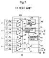
- Fig. 7 illustrates the detailed configuration of the conventional drive circuit 15 shown in Fig. 6a and the various signals it receives from and transmits to the read channel LSI 102.
- the circuit 15 comprises a read/write circuit 200, a read postamplifier 23, a read/write switching circuit 34, a head selection circuit 35, and a write current generation circuit 36.
- the read/write circuit 200 comprises write drivers 26 to 29 and read preamplifiers 30 to 33.
- the magnetic heads 3 to 6 respectively contain write heads 3a to 6a and read heads 3b to 6b.
- a chip selection signal 57 and a read/write selection signal 56 are supplied from an external control circuit (e.g. the read channel LSI 102) to the read/write switching circuit 34.
- the chip selection signal 57 enables the drive circuit 15 and sets it in an operational state, and the read/write selection signal 56 indicates whether a read operation or a write operation is to be performed.
- the signal 56 indicates that a write operation is to be performed.
- the switching circuit 34 outputs a read/write mode signal indicating that a write operation is to be performed.
- the external control circuit also outputs a two bit head selection signal 51 and 52 to the head selection circuit 35 for selecting one of the four heads 3 to 6.
- the circuit 35 inputs the signal 51 and 52 and determines that the magnetic head 3 has been selected to perform a read or write operation. As a result, the circuit 35 outputs an enable signal to enable the write driver 26 and read preamplifier 30 which are connected to the magnetic head 3.
- the write current generation circuit 36 inputs the read/write mode signal from the read/write switching circuit 34, a predetermined write bias current, and a write data signal 53.
- the predetermined write bias current is generated by connecting an external resistor 55 between the write current terminal 54 and ground. Since the read/write mode signal from the circuit 34 indicates a write mode, the generation circuit 36 outputs the predetermined write bias current based on the write data 53 to the write drivers 26 to 29. Since the enable signal output from the head selection circuit 35 enables the write driver 26, the write driver 26 drives the write head 3a with the write bias current output from the generation circuit 36 to write data to the magnetic disk 1. For example, if a logic "1" is to be written to the disk 1, the write driver causes the write bias current to travel in one direction through the write head 3a. On the other hand, if a logic "0" is to be written to the disk 1, the write driver causes the write bias current to travel in the other direction through the write head 3a.
- the chip selection signal 57 sets the drive circuit 15 in an operational state, and the read/write selection signal 56 indicates that a read operation is to be performed. As a result, the switching circuit 34 outputs a read/write mode signal indicating a read mode.
- the circuit 35 inputs the head selection signal 51 and 52 and determines that the magnetic head 3 has been selected to perform a read or write operation and enables the write driver 26 and read preamplifier 30.
- the read preamplifier 30 inputs a predetermined read current and applies a read bias current to the read head 3b based on the predetermined read current so that the head 3b reads data from the disk 1 and supplies it to the preamplifier 30.
- the predetermined read current is generated by connecting an external resistor 61 between the read current terminal 60 and ground.
- the preamplifier 30 amplifies the signal received from the head 3b and supplies the amplified signal to the postamplifier 23.
- the read head 3b may be a magnetic-to-electrical resistor which changes resistance based on the magnetic field applied to the resistor. Thus, when a logic "0" on the disk passes by the head 3b, the head 3b has one resistance, and when a logic "1" on the disk passes by the head 3b, the head 3b has another resistance. Thus, the read bias current flowing through the head 3b changes depending on the read data, and thus, the value of the data can be determined based on the changing current. Since the read/write mode signal from the circuit 34 indicates a read mode, the postamplifier 23 amplifies the signal from the preamplifier 30 and outputs it as read data 58 and 59.
- the above example illustrates the operation of the drive circuit 15 when data is written to the disk 1 via the write head 3a and when data is read from the disk 1 via the read head 3b. Also, the circuit 15 operates in a similar manner when data is being written via the write heads 4a to 6a and when data is being read via the read heads 4b to 6b.
- One method of increasing such capacity is to increase the frequency of the write data signal so that a larger amount of data can be stored in a fixed area of a magnetic disk.
- the recording frequency can be raised by decreasing the inductance of the write head.
- the inductance of the write head decreases, the level of stray inductance which will adversely affect the write operation also decreases.
- the write head is unable to properly write data to the disk if the amount of stray inductance surrounding the write head exceeds 10% of the inductance of the write head itself. Therefore, by lowering the inductance of the head, the sensitivity of the head to stray inductance increases, and thus, the recording frequency of data cannot be increased beyond a certain point by lowering the inductance of the write head.
- the chip area of the circuit 15 is large because many external components must be connected to the drive circuit 15, and thus, the wiring surrounding the drive circuit 15 becomes complicated.
- the distance between the drive circuit 15 and the magnetic heads 3 to 6 is relatively large, and thus, a substantial amount of stray inductance is present around the heads 3 to 6. Accordingly, the size of the heads 3 to 6 cannot be significantly reduced, and the recording frequency of the drive circuit 15 cannot be significantly increased.
- the size of the drive circuit must be increased to adequately separate the terminals to avoid a signal crosstalk between the signals input to and output from the terminals. Accordingly, a large amount of stray inductance exists around the drive circuit 15.
- the inductance of the heads 3 to 6 must be relatively high. As a result, the storage capacity of the disk drive and recording frequency of the drive circuit 15 cannot be increased.
- the effects of the stray inductance may be avoided by separating the drive circuit 15 and the heads 3 to 6 via a large distance. However, in such case, the size of the hard disk drive cannot be made compact.
- An object of the present invention is to provide a drive circuit for a magnetic recording device in which the stray capacitance and stray inductance of peripheral wiring of the drive circuit is reduced.
- Another object of the present invention is to increase the read/write frequency of data of a magnetic recording device.
- a further object of the present invention is to increase the recording density of the magnetic recording device.
- An additional object of the present invention is to provide a drive circuit for a magnetic recording device in which the operation characteristics do not deteriorate when the peripheral wiring of the drive circuit is formed by a high-impedance metal evaporation process.
- a still further object of the present invention is to provide a drive circuit for a magnetic recording device in which the write bias current and read bias current can be easily optimized to the most appropriate current value.
- a drive circuit for a magnetic recording device comprises: a write driver which inputs write data and outputs a corresponding writing current to a write head to store information onto a magnetic disk; a read preamplifier which supplies a bias current to a read magnetic head to sense information stored on said magnetic disk and which amplifies said information as output data; a write predriver which inputs a write data signal via a data signal line and a write mode signal and which supplies said write data to said write driver based on said write mode signal; a read postamplifier which inputs said output data and a read mode signal and which amplifies said output data to produce a read data signal based on said read mode signal; and a current signal detecting circuit which inputs an external current setting signal via said data signal line and generates a current value signal based on said external current setting signal.
- a drive circuit for a magnetic recording device comprises: a write driver which is driven by said a current setting signal, inputs write data, and outputs a corresponding writing current to a write head to store information onto a magnetic disk; a read preamplifier which is driven by a bias current setting signal, supplies a bias current to a read magnetic head to sense information stored on said magnetic disk, and amplifies said information as output data; a write predriver which inputs a write data signal via a data signal line and a write mode signal and which supplies said write data to said write driver based on said write mode signal; a read postamplifier which inputs said output data and a read mode signal and which amplifies said output data to produce a read data signal based on said read mode signal; a current signal detecting circuit which inputs an external current setting signal via said data signal line and generates a current value signal based on said external current setting signal; a mode selection circuit which inputs a control signal
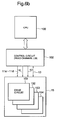
- Fig. 1 illustrates a magnetic recording device (i.e. a hard disk drive) which incorporates a drive circuit according to a first embodiment of the present invention.
- the disk drive comprises first and second disks 1 and 2, magnetic heads 3 to 6, and drive circuits 151 to 154.
- the magnetic head 3 is disposed near an upper surface of the first disk 1, and the magnetic head 4 is disposed near a lower surface of the first disk 1.
- the magnetic head 5 is disposed near an upper surface of the second disk 2, and the magnetic head 6 is disposed near a lower surface of the second disk 2.
- the heads 3 to 6 move with respect to the surfaces of the disks 1 and 2 and can read and write data to and from the disks 1 and 2.
- the heads 3 to 6 are respectively connected to swing arms (not shown) and can be moved in the radial direction of the disks 1 and 2 by moving the swing arms within a swing arm movement range 9.
- Drive circuits 151 to 154 are respectively disposed very close to the magnetic heads 3 to 6 and control the reading and writing operations of the heads 3 to 6. Also, the drive circuits 151 to 154 may be respectively packaged on the actual swing arms on which the heads 3 to 6 are mounted by using a bump technique. In the bump technique, solder is put on the swing arms, and the drive circuits 151 to 154 are mounted on the swing arms via the solder near the heads 3 to 6.
- control signals 12 are input via a control signal terminal 12A and output to all of the drive circuits 151 to 154 in parallel.
- data signals 13 are input via a data signal terminal 13A and output to all of the circuits 151 to 154 in parallel.
- data signals 13 may be output from the circuits 151 to 154 via the terminals 13A.
- each of the four drive circuits 151 to 154 are connected to a ground signal 14 via a ground terminal 14A and are supplied with power signals 11a to 11d from a power source.
- the power signals 11a to 11d are respectively connected to power source drive terminals within the drive circuits 151 to 154 to supply power to the circuits 151 to 154.
- the power signals 11a to 11d serve as chip select signals for selectively activating one of the circuits 151 to 154 by only supplying one of the signals 11a to 11d to one (or none) of the circuits 151 to 154 at any given instant.
- Fig. 2a shows an illustrative example of the structure of the drive circuit 151. Also, since the circuits 152 to 154 have a similar structure, a description of such circuits 152 to 154 is omitted for the sake of brevity. Also, Fig. 3 illustrates various signals input to or output from the drive circuit 151.
- the drive circuit 151 comprises a write driver 18, a write predriver 19, a current setting circuit 20, a control circuit 21, a read preamplifier 22, and a read postamplifier 23.
- the magnetic head 3 comprises a write head 3a and a read head 3b.
- a power signal 11a is selectively applied to the power source terminal (not shown) of the drive circuit 151 as a chip select signal to selectively activate such circuit 151 at a certain time. (Fig. 3a). In other words, none of the other power signals 11b to 11d are respectively supplied to the drive circuits 152 to 154.
- the control circuit 21 After receiving the power signal 11a, the control circuit 21 begins operating and inputs the control signal 12. As shown in Fig. 3b, the control signal 12 supplies a basic clock signal during a first period T0, supplies a two-bit read/write mode control signal during a second period T1, and supplies a five-bit current setting signal during the period T2.
- the basic clock signal is a ten-bit square wave having ten pulses.
- the control circuit 21 inputs the basic clock signal and synchronizes its operations based on the timing of the basic clock signal.
- the control circuit 21 may comprise a phase lock loop ("PLL") circuit 21a, a shift register 21b, and a decoder circuit 21c.
- the PLL circuit 21a receives the clock signal during the period T0 and appropriately synchronizes the various components of the control circuit 21 with the clock signal.
- the shift register 21b serially inputs the two-bit read/write mode control signal during the period T1 and the five-bit current setting signal during the period T2.
- the register 21b After receiving such signals, the register 21b outputs the read/write mode control signal from its bit positions 1 and 2 to the decoder circuit 21c. Then, the decoder circuit 21c decodes the two-bit signal to generate a write mode signal "b" and a read mode signal "d". Since a write operation is to be performed, the control circuit 21 outputs the write mode signal "b" to the write driver 18 and the write predriver 19 to activate the predriver 19. The signals "b” and “d” may be output via a common control signal line to the write driver 18, the write predriver 19, the read preamplifier 22, and the read postamplifier 23.
- the driver 18 and predriver 19 may be activated when a logic "1" is output on the common control signal line (i.e. the write mode signal "b” is output), and the preamplifier 22 and postamplifier 23 may be activated when a logic "0" is output on the common signal line (i.e. the read mode signal “d” is output).
- the signals "b” and “d” may be output via two different control signal lines.
- the five-bit current setting signal is supplied from bit positions 3 to 7 of the shift register 21b to the current setting circuit 20.
- the current setting circuit 20 comprises a digital-to-analog ("D/A") converter 20a, and the D/A converter 20a converts the five bit current setting signal into an analog current. Then, the analog current is output as the write current setting signal "a" and the bias current setting signal "c".
- D/A digital-to-analog
- a write data signal 13 is provided on the data signal line 13A. Since the write driver 18 and the write predriver 19 are activated via the write mode signal "b" during a write operation, the predriver 19 inputs the data signal 13, processes the data signal 13, and outputs corresponding write data. Then, the write driver 18 inputs the write data and generates a write bias current based on the write current setting signal and the value of the write data. As a result, the write head 3a writes data to the first disk 1 based on the write bias current.
- a power signal 11a is selectively applied to the power source terminal (not shown) of the drive circuit 151 as a chip select signal to selectively activate such circuit 151 at a certain time.
- the control circuit 21 starts to input the control signal 12. Specifically, the circuit 21 synchronizes its operations in accordance with the basic clock signal during the period T0 and inputs the two-bit read/write mode and the five-bit current setting signal during the periods T1 and T2 (Fig. 3b).
- the two-bit read/write mode signal is decoded to generate a write mode signal "b" and a read mode signal "d". Since a read operation is to be performed, the control circuit 21 outputs the read mode signal "d" to the read preamplifier 22 and the read postamplifier 23 to activate the preamplifier 22 and postamplifier 23.
- the five-bit current setting signal is supplied to the current setting circuit 20 and converted into an analog current via the D/A converter 20a. Then, the analog current is output as the write current setting signal "a” and the bias current setting signal "c".
- the read preamplifier 22 When the read preamplifier 22 inputs the bias current setting signal "c", it applies a read bias current to the read head 3b. As a result, the head 3b reads data from the disk 1 and supplies it to the preamplifier 22. Then, the preamplifier 22 amplifies the signal and supplies it as output data to the read postamplifier 23. Since the postamplifier 23 is activated by the read mode signal "d", the postamplifier 23 amplifies the output data and outputs it to the data signal line 13A as a read data signal 13. (Fig. 3c).
- the above example illustrates the operation of the drive circuit 151 when data is written to the disk 1 via the write head 3a and when data is read from the disk 1 via the read head 3b.
- the remaining drive circuits 152 to 154 operate in a similar manner when data is being written via the write heads 4a to 6a and when data is being read via the read heads 4b to 6b.
- the drive circuits 151 to 154 contain a current setting circuit 20 for generating the currents supplied to the write driver 18 and the read preamplifier 22, and thus, they do not need to utilize the external resistors 55 and 61 shown in Fig. 7 to generate such currents. Also, since the drive circuits 151 to 154 are activated by selectively applying one of the power signals 11a to 11d as a chip selection signal to one of the circuits 151 to 154, the drive circuits 151-154 do not need to input a signal which is analogous to the chip selection signal 57 shown in Fig. 7.
- each of the individual magnetic heads 3 to 6 corresponds to only one of the respective drive circuits 151 to 154, the power signals 11a to 11d which selectively activate one of the circuits 151 to 154 effectively selects one of the heads 3 to 6. Therefore, the head selection signals 51 and 52 shown in Fig. 7 are unnecessary.
- the drive circuits 151 to 154 input and output the read and write data signals 13 via a common data signal line 13A. Therefore, the circuits 151 to 154 do not need to use two separate data signal lines as in the conventional device shown in Fig. 7.
- the drive circuits 151 to 154 of the first embodiment only need to input four signal lines: a control signal line 12, a data signal line 13, a power signal line, and a ground signal line.
- the conventional drive circuit 15 shown in Fig. 7 needs to input nine signal lines: two head selection signal lines 51 and 52, a write data signal line 53, a write current setting signal line 54, a read/write selection signal line 56, a chip selection signal line 57, two read data signal lines 58 and 59, and a read current setting signal line 60.
- the number of signal lines are dramatically reduced.
- the conventional drive circuit 15 shown in Fig. 7 needs four write drivers 26 to 29 and four read preamplifiers 30 to 33 in one semiconductor chip.
- the first embodiment loads only a write driver 18 and a read preamplifier 22 in one semiconductor chip. Therefore, the chip area of each drive circuit 151 to 154 of the embodiment can be reduced to a quarter of the size of the conventional drive circuit 15.
- the drive circuits 151 to 154 can be disposed very close to the magnetic heads 3 to 6 near the ends of the swing arms. Accordingly, the wires between the circuits 151 to 154 and the heads 3 to 6 are very short and thus, generate very little stray capacitance and stray inductance. Therefore, the inductance of the magnetic heads 3 to 6 can be reduced, and the frequency of data writing and data reading operations can be substantially increased. As a result, the recording density of a magnetic recording device can also be increased.
- the conventional drive circuit 15 shown in Fig. 7 thick wires are necessary to suppress the stray capacitance and the inductance generated by the many signals transmitted from the circuit 15 to the magnetic heads 3 to 6 and the other external components.
- the wiring between the magnetic heads 3 to 6 and the drive circuits 151 to 154 are short and only carry small signals. Since the signals are small, the stray capacitance and inductance is extremely small, and thus, compensating for such capacitance and inductance is unnecessary.
- the read data signals 13 are barely affected by stray capacitance and stray inductance because they correspond to data which has been amplified by the postamplifier 30. Also, the write data signals 13 input to the circuits 151 to 154 are barely affected by the stray capacitance and inductance because they are digital data signals.
- integrated wirings which are manufactured via an evaporation process, a metal sputtering process, or other semiconductor manufacturing process can be used as the wirings between the drive circuits 151 to 154 and the magnetic heads 3 to 6 and the wirings between the circuits 151 to 154 and the external devices.
- the read and write setting currents supplied to the write drivers 26 to 29 and the preamplifiers 30 to 33 are generated by connecting resistors 55 and 61 to the circuit 15.
- the current setting circuit 20 is incorporated into the circuits 151 to 154, and a value of the current is set by a D/A converter based on serial data received from an external device. By feeding back the serial read data signal 13 to the external device, the device can evaluate the current level. Then, the external device can change the value of the current setting signal transmitted during the second period T2 of the control signal 12 to optimize the value of the current setting signals "a" and "c" supplied to the write driver 18 and the preamplifier 22, respectively. For example, if the external device (i.e. a CPU) outputs "1010" to be written to the disk, the CPU reads the same data from the disk. If the read data is different from the written data, the CPU increases the current setting signals "a" and "c".
- the external device i.e. a CPU
- Fig. 4a shows an illustrative example of the structure of the drive circuit 151 according to a second embodiment of the present invention. Also, since the circuits 152 to 154 have a similar structure, a description of such circuits 152 to 154 is omitted for the sake of brevity. Also, Fig. 5 illustrates various signals input to or output from the drive circuit 151.
- the drive circuit 151 comprises a write driver 18, a write predriver 19, a current setting circuit 20, a read preamplifier 22, a read postamplifier 23, a counter circuit 24, and a mode selection circuit 25.
- the magnetic head 3 comprises a write head 3a and a read head 3b.
- a power signal 11a is selectively applied to the power source terminal (not shown) of the drive circuit 151 as a chip select signal to selectively activate such circuit 151 at a certain time. (Fig. 5a). In other words, none of the other power signals 11b to 11d are respectively supplied to the drive circuits 152 to 154.
- the mode selection circuit 25 inputs the control signal 12 and determines if the drive circuit 151 is operating in a write mode or a read mode based on the signal 12.
- the signal 12 may identify a write mode if it equals "0" and may identify a read mode if it equals "1".
- the mode selection circuit 25 comprises a read/write decoder 25a and a one shot circuit 25b.
- the decoder 25a is enabled by the power signal 11a, inputs the control signal 12, and outputs the write mode signal "b” or the read mode signal "d” based on the value of the control signal 12.
- the signals "b” and “d” may actually be the same signal but may have different values based on the values of the control signal 12.
- the mode selection circuit 25 may simply pass on the control signal as the signals "b” and "d”.
- the one shot circuit 25b has a time constant such that it outputs a one shot signal when the power signal 11a is initially applied to it and remains activated only for a time which corresponds to a current setting read period T4. (See Fig. 5c).
- the counter circuit 24 comprises a transistor 24a and a binary counter 24b.
- the transistor 24a inputs the data signal 13 via its source and inputs the one shot signal via its gate. As a result, the transistor 24a only outputs the data signal when the one shot signal is being output from the one shot circuit 25b (i.e. only during the period T4).
- the binary counter 24b inputs the data signal 13 during the period T4 and counts the pulses contained in the data signal 13. As shown in Fig. 5c, the data signal 13 initially supplies a current setting signal C1 during the current setting read period T4 and then supplies a data signal D0, D1, D2, D3, etc. after the period T4.
- the binary counter 24a only counts the number of pulses in the current setting signal C1 and outputs a corresponding count value. Also, the counter 24a inputs the power signal 11a and is reset when the power signal 11a is not activated. Therefore, whenever the signal 11a is initially applied to the drive circuit 151, the count value of the counter 24b equals zero.
- the current setting circuit 20 comprises a D/A converter 20a which inputs the count value and converts it into an analog current. Then, the analog current is output as the write current setting signal "a" and the bias current setting signal "c". Thus, by varying the number of pulses contained in the current setting signal C1, value of the setting current signals "a” and “c" can be changed.
- a write data signal 13 is provided on the data signal line 13A after the period T4. Since the write driver 18 and the write predriver 19 are activated via the write mode signal "b" during the write mode, the predriver 19 inputs the data signal 13, processes the data signal, and outputs corresponding write data. Then, the write driver 18 inputs the write data and generates a write bias current based on the write current setting signal "a" and the value of the write data. As a result, the write head 3a writes data to the first disk 1 based on the write bias current.
- the power signal 11a is applied to the drive circuit 151.
- the counter circuit 24 counts the pulses of the current setting signal C1 during the period T4 and generates a corresponding count value.
- the current setting circuit 20 generates the write current setting signal "a” and the bias current setting signal "c” based on the count value.
- the mode selection circuit 25 inputs the control signal 12 and outputs the write mode signal "b” or the read mode signal "d” based on the value of the control signal 12.
- the read preamplifier 22 When the read preamplifier 22 inputs the bias current setting signal "c", it applies a read bias current to the read head 3b. As a result, the head 3a reads data from the disk 1 and supplies it to the preamplifier 22. Since the preamplifier 22 is activated by the read mode signal "d”, it amplifies the data and supplies it as output data to the read postamplifier 23. Also, since the postamplifier 23 is activated by the read mode signal "d", the postamplifier 23 amplifies the output data and outputs it to the data signal line 13A as a read data signal 13. (Fig. 5c).
- the above example illustrates the operation of the drive circuit 151 when data is written to the disk 1 via the write head 3a and when data is read from the disk 1 via the read head 3b.
- the remaining drive circuits 152 to 154 operate in a similar manner when data is being written via the write heads 4a to 6a and when data is being read via the read heads 4b to 6b.
- the drive circuits 151 to 154 of the second embodiment are further simplified and the chip area is further decreased. Specifically, in the second embodiment, the drive circuits 151 to 154 do not need to be synchronized with a basic clock signal contained in the control signal 12, and therefore, no need exists to incorporate a control circuit 21 containing a PLL circuit.
Landscapes
- Digital Magnetic Recording (AREA)
Applications Claiming Priority (3)
| Application Number | Priority Date | Filing Date | Title |
|---|---|---|---|
| JP9172389A JP3001466B2 (ja) | 1997-06-27 | 1997-06-27 | 磁気記録装置の駆動回路 |
| JP172389/97 | 1997-06-27 | ||
| JP17238997 | 1997-06-27 |
Publications (2)
| Publication Number | Publication Date |
|---|---|
| EP0887789A2 true EP0887789A2 (de) | 1998-12-30 |
| EP0887789A3 EP0887789A3 (de) | 2005-06-29 |
Family
ID=15941031
Family Applications (1)
| Application Number | Title | Priority Date | Filing Date |
|---|---|---|---|
| EP98111881A Withdrawn EP0887789A3 (de) | 1997-06-27 | 1998-06-26 | Treiberschaltungen für eine Magnetaufzeichnungsvorrichtung |
Country Status (8)
| Country | Link |
|---|---|
| US (2) | US6292321B1 (de) |
| EP (1) | EP0887789A3 (de) |
| JP (1) | JP3001466B2 (de) |
| KR (1) | KR100328747B1 (de) |
| CN (1) | CN1124600C (de) |
| CA (1) | CA2242100C (de) |
| SG (1) | SG70643A1 (de) |
| TW (1) | TW385430B (de) |
Families Citing this family (9)
| Publication number | Priority date | Publication date | Assignee | Title |
|---|---|---|---|---|
| JP2002015403A (ja) * | 2000-06-30 | 2002-01-18 | Sony Corp | ヘッド装置、ハードディスク装置および記録再生装置 |
| US6717759B1 (en) * | 2001-02-16 | 2004-04-06 | Maxtor Corporation | Hindering PTP in a hard disk |
| JP2003223702A (ja) * | 2002-01-28 | 2003-08-08 | Hitachi Ltd | 媒体記録再生システムおよびそれに用いられる半導体集積回路 |
| JP2005108370A (ja) * | 2003-10-01 | 2005-04-21 | Hitachi Global Storage Technologies Netherlands Bv | メディア駆動装置、メディアへのデータ記録の処理方法、メディアから読み出したデータの処理方法及びメディアからのデータ読み出し処理の制御方法 |
| US7701654B2 (en) * | 2005-09-23 | 2010-04-20 | Agere Systems Inc. | Apparatus and method for controlling common mode voltage of a disk drive write head |
| CN102312431A (zh) * | 2011-04-26 | 2012-01-11 | 王庆伟 | 螺齿组合桩及成桩工法 |
| DE102014100212B4 (de) | 2013-01-11 | 2018-04-05 | Bumotec Sa | Bearbeitungseinheit mit zwei Arbeitsspindeln und Fertigungsstraße |
| DE202013000225U1 (de) | 2013-01-11 | 2014-04-14 | Bumotec Sa | Bearbeitungseinheit mit zwei Arbeitsspindeln |
| JP2021034080A (ja) * | 2019-08-23 | 2021-03-01 | 株式会社東芝 | 磁気ディスク装置、および該磁気ディスク装置の動作モード規定方法 |
Family Cites Families (12)
| Publication number | Priority date | Publication date | Assignee | Title |
|---|---|---|---|---|
| FR2559297B1 (fr) * | 1984-02-03 | 1990-01-12 | Commissariat Energie Atomique | Nouveau patin de vol pour tetes magnetiques d'enregistrement |
| US4656538A (en) * | 1985-11-14 | 1987-04-07 | Xebec Development Partners, Ltd. | Disk drive control system |
| US4688119A (en) * | 1985-11-20 | 1987-08-18 | Xebec Development Partners, Ltd. | Detection and amplification circuit |
| KR940011436B1 (ko) * | 1989-04-19 | 1994-12-15 | 가부시끼가이샤 히다찌세이사꾸쇼 | 자기디스크 기억장치 |
| US5055969A (en) * | 1990-09-28 | 1991-10-08 | Seagate Technology, Inc. | Servo/data actuator arm flexible circuit |
| US5245489A (en) * | 1990-10-04 | 1993-09-14 | Hitachi, Ltd. | Guide arm with a fixed printed circuit board for magnetic disk drive |
| US5430584A (en) * | 1991-10-18 | 1995-07-04 | International Microelectronic Products | Disk drive interface combining a magneto-resistive read and inductive write circuits |
| JP3109889B2 (ja) * | 1992-01-30 | 2000-11-20 | 株式会社日立製作所 | 磁気ヘッド用回路 |
| JPH07176002A (ja) * | 1993-11-08 | 1995-07-14 | Toshiba Corp | 磁気ディスク装置 |
| US5546030A (en) * | 1994-12-30 | 1996-08-13 | Sgs-Thomson Microelectronics, Inc. | Differential high speed inductive driver with a bidirectional current limiting output stage |
| WO1997009714A1 (en) * | 1995-09-06 | 1997-03-13 | Seagate Technology, Inc. | Dynamically programmable magneto-resistive head write and read bias currents |
| US6268160B1 (en) * | 1997-08-28 | 2001-07-31 | Medical Research Council | Method of screening for anti-malarial compounds |
-
1997
- 1997-06-27 JP JP9172389A patent/JP3001466B2/ja not_active Expired - Fee Related
-
1998
- 1998-06-25 TW TW087110332A patent/TW385430B/zh not_active IP Right Cessation
- 1998-06-26 US US09/105,267 patent/US6292321B1/en not_active Expired - Lifetime
- 1998-06-26 EP EP98111881A patent/EP0887789A3/de not_active Withdrawn
- 1998-06-26 CA CA002242100A patent/CA2242100C/en not_active Expired - Fee Related
- 1998-06-26 SG SG1998001530A patent/SG70643A1/en unknown
- 1998-06-27 CN CN98103385A patent/CN1124600C/zh not_active Expired - Fee Related
- 1998-06-27 KR KR1019980024627A patent/KR100328747B1/ko not_active Expired - Fee Related
-
2001
- 2001-07-23 US US09/909,802 patent/US6469857B2/en not_active Expired - Fee Related
Also Published As
| Publication number | Publication date |
|---|---|
| EP0887789A3 (de) | 2005-06-29 |
| SG70643A1 (en) | 2000-02-22 |
| JPH1116112A (ja) | 1999-01-22 |
| CA2242100A1 (en) | 1998-12-27 |
| US6292321B1 (en) | 2001-09-18 |
| KR100328747B1 (ko) | 2002-06-20 |
| TW385430B (en) | 2000-03-21 |
| US20010040747A1 (en) | 2001-11-15 |
| CA2242100C (en) | 2001-03-27 |
| JP3001466B2 (ja) | 2000-01-24 |
| US6469857B2 (en) | 2002-10-22 |
| KR19990007414A (ko) | 1999-01-25 |
| CN1124600C (zh) | 2003-10-15 |
| CN1211037A (zh) | 1999-03-17 |
Similar Documents
| Publication | Publication Date | Title |
|---|---|---|
| US6496317B2 (en) | Accurate adjustable current overshoot circuit | |
| US5430584A (en) | Disk drive interface combining a magneto-resistive read and inductive write circuits | |
| EP1399919B1 (de) | Schreibausgangstreiber mit internen programmierbaren pull-up-widerständen | |
| US6271978B1 (en) | Power efficient overshoot control for magnetic recording write driver | |
| US6292321B1 (en) | Drive circuits for a magnetic recording device | |
| CN104575526A (zh) | 具有提供模式相关写功能的驱动器控制器的存储设备 | |
| JP2005222684A (ja) | 書込みヘッド消磁方法および装置 | |
| EP1417763B1 (de) | Niederspannungs-ladungspumpe zur verwendung in einem phasenregelkreis | |
| US20020176190A1 (en) | View DAC feedback inside analog front circuit | |
| US5987542A (en) | Serial interface circuit for adaptively supporting the serial interface of read/write channel circuits in a magnetic disk drive | |
| US7035027B2 (en) | Circuits to achieve high data rate writing on thin film transducer | |
| US6400190B1 (en) | Controlled current undershoot circuit | |
| JP2000182203A (ja) | ハ―ドディスク・ドライブ書込みヘッドの調節可能なライタ―・オ―バ―シュ―ト | |
| US7787206B2 (en) | Systems and methods for accessing preamp registers using commands via read channel/hard disk controller interface | |
| US6597302B2 (en) | System for increasing the bandwidth of sample-and-hold circuits in flash ADCs | |
| JP2595806B2 (ja) | 磁気ディスク装置のリード・ライトアンプ回路 | |
| US6700721B2 (en) | Magnetic recording and reproducing apparatus and semiconductor integrated circuit for use in the same comprising a read/write signal processor having an interleave write data generator | |
| US7336547B2 (en) | Memory device having conditioning output data | |
| US20040120065A1 (en) | Impedance-matched write driver circuit and system using same | |
| US20030142432A1 (en) | Storage media reading system and semiconductor integrated circuit device | |
| US6594101B1 (en) | Read head protection circuit and method | |
| US20010022699A1 (en) | Differentially driven, current mirror based coil driver | |
| US6031807A (en) | Programming the inductance of read/write heads | |
| US20040218301A1 (en) | Low Power Servo Mode Write Driver | |
| US20050094306A1 (en) | Impedance-matched write driver circuit and system using same |
Legal Events
| Date | Code | Title | Description |
|---|---|---|---|
| PUAI | Public reference made under article 153(3) epc to a published international application that has entered the european phase |
Free format text: ORIGINAL CODE: 0009012 |
|
| AK | Designated contracting states |
Kind code of ref document: A2 Designated state(s): AT BE CH CY DE DK ES FI FR GB GR IE IT LI LU MC NL PT SE |
|
| AX | Request for extension of the european patent |
Free format text: AL;LT;LV;MK;RO;SI |
|
| RAP1 | Party data changed (applicant data changed or rights of an application transferred) |
Owner name: NEC ELECTRONICS CORPORATION |
|
| PUAL | Search report despatched |
Free format text: ORIGINAL CODE: 0009013 |
|
| AK | Designated contracting states |
Kind code of ref document: A3 Designated state(s): AT BE CH CY DE DK ES FI FR GB GR IE IT LI LU MC NL PT SE |
|
| AX | Request for extension of the european patent |
Extension state: AL LT LV MK RO SI |
|
| 17P | Request for examination filed |
Effective date: 20050519 |
|
| AKX | Designation fees paid |
Designated state(s): DE FR |
|
| RAP1 | Party data changed (applicant data changed or rights of an application transferred) |
Owner name: RENESAS ELECTRONICS CORPORATION |
|
| STAA | Information on the status of an ep patent application or granted ep patent |
Free format text: STATUS: THE APPLICATION HAS BEEN WITHDRAWN |
|
| 18W | Application withdrawn |
Effective date: 20120323 |