EP0881641A2 - Appareil de disques optique et méthode d'enregistrement de données - Google Patents
Appareil de disques optique et méthode d'enregistrement de données Download PDFInfo
- Publication number
- EP0881641A2 EP0881641A2 EP98303843A EP98303843A EP0881641A2 EP 0881641 A2 EP0881641 A2 EP 0881641A2 EP 98303843 A EP98303843 A EP 98303843A EP 98303843 A EP98303843 A EP 98303843A EP 0881641 A2 EP0881641 A2 EP 0881641A2
- Authority
- EP
- European Patent Office
- Prior art keywords
- data
- signal
- bits
- optical disk
- frequency
- Prior art date
- Legal status (The legal status is an assumption and is not a legal conclusion. Google has not performed a legal analysis and makes no representation as to the accuracy of the status listed.)
- Withdrawn
Links
- 230000003287 optical effect Effects 0.000 title claims abstract description 35
- 238000000034 method Methods 0.000 title claims description 50
- 230000008569 process Effects 0.000 claims description 34
- 238000012545 processing Methods 0.000 claims description 23
- 238000010276 construction Methods 0.000 description 22
- 238000010586 diagram Methods 0.000 description 15
- 238000012937 correction Methods 0.000 description 5
- 238000001514 detection method Methods 0.000 description 4
- 238000009825 accumulation Methods 0.000 description 3
- 230000008859 change Effects 0.000 description 3
- 230000001360 synchronised effect Effects 0.000 description 3
- 230000015572 biosynthetic process Effects 0.000 description 2
- 239000013078 crystal Substances 0.000 description 2
- 230000006870 function Effects 0.000 description 2
- 230000007246 mechanism Effects 0.000 description 2
- 238000012986 modification Methods 0.000 description 2
- 230000004048 modification Effects 0.000 description 2
- 230000010355 oscillation Effects 0.000 description 2
- 238000012546 transfer Methods 0.000 description 2
- 230000032683 aging Effects 0.000 description 1
- 238000006243 chemical reaction Methods 0.000 description 1
- 238000004891 communication Methods 0.000 description 1
- 238000000354 decomposition reaction Methods 0.000 description 1
- 238000004049 embossing Methods 0.000 description 1
- 238000003780 insertion Methods 0.000 description 1
- 230000037431 insertion Effects 0.000 description 1
- ZMRUPTIKESYGQW-UHFFFAOYSA-N propranolol hydrochloride Chemical compound [H+].[Cl-].C1=CC=C2C(OCC(O)CNC(C)C)=CC=CC2=C1 ZMRUPTIKESYGQW-UHFFFAOYSA-N 0.000 description 1
- 238000005070 sampling Methods 0.000 description 1
Images


Classifications
-
- G—PHYSICS
- G11—INFORMATION STORAGE
- G11B—INFORMATION STORAGE BASED ON RELATIVE MOVEMENT BETWEEN RECORD CARRIER AND TRANSDUCER
- G11B27/00—Editing; Indexing; Addressing; Timing or synchronising; Monitoring; Measuring tape travel
- G11B27/10—Indexing; Addressing; Timing or synchronising; Measuring tape travel
- G11B27/19—Indexing; Addressing; Timing or synchronising; Measuring tape travel by using information detectable on the record carrier
- G11B27/28—Indexing; Addressing; Timing or synchronising; Measuring tape travel by using information detectable on the record carrier by using information signals recorded by the same method as the main recording
- G11B27/30—Indexing; Addressing; Timing or synchronising; Measuring tape travel by using information detectable on the record carrier by using information signals recorded by the same method as the main recording on the same track as the main recording
- G11B27/3027—Indexing; Addressing; Timing or synchronising; Measuring tape travel by using information detectable on the record carrier by using information signals recorded by the same method as the main recording on the same track as the main recording used signal is digitally coded
-
- G—PHYSICS
- G11—INFORMATION STORAGE
- G11B—INFORMATION STORAGE BASED ON RELATIVE MOVEMENT BETWEEN RECORD CARRIER AND TRANSDUCER
- G11B20/00—Signal processing not specific to the method of recording or reproducing; Circuits therefor
- G11B20/10—Digital recording or reproducing
- G11B20/10009—Improvement or modification of read or write signals
- G11B20/10222—Improvement or modification of read or write signals clock-related aspects, e.g. phase or frequency adjustment or bit synchronisation
-
- G—PHYSICS
- G11—INFORMATION STORAGE
- G11B—INFORMATION STORAGE BASED ON RELATIVE MOVEMENT BETWEEN RECORD CARRIER AND TRANSDUCER
- G11B20/00—Signal processing not specific to the method of recording or reproducing; Circuits therefor
- G11B20/10—Digital recording or reproducing
- G11B20/10009—Improvement or modification of read or write signals
-
- G—PHYSICS
- G11—INFORMATION STORAGE
- G11B—INFORMATION STORAGE BASED ON RELATIVE MOVEMENT BETWEEN RECORD CARRIER AND TRANSDUCER
- G11B20/00—Signal processing not specific to the method of recording or reproducing; Circuits therefor
- G11B20/10—Digital recording or reproducing
- G11B20/12—Formatting, e.g. arrangement of data block or words on the record carriers
- G11B20/1217—Formatting, e.g. arrangement of data block or words on the record carriers on discs
-
- G—PHYSICS
- G11—INFORMATION STORAGE
- G11B—INFORMATION STORAGE BASED ON RELATIVE MOVEMENT BETWEEN RECORD CARRIER AND TRANSDUCER
- G11B2220/00—Record carriers by type
- G11B2220/20—Disc-shaped record carriers
-
- G—PHYSICS
- G11—INFORMATION STORAGE
- G11B—INFORMATION STORAGE BASED ON RELATIVE MOVEMENT BETWEEN RECORD CARRIER AND TRANSDUCER
- G11B2220/00—Record carriers by type
- G11B2220/20—Disc-shaped record carriers
- G11B2220/25—Disc-shaped record carriers characterised in that the disc is based on a specific recording technology
- G11B2220/2525—Magneto-optical [MO] discs
- G11B2220/2529—Mini-discs
Definitions
- the invention relates to optical disk apparatus and data recording method, in which physical address information is previously recorded on an optical disk and by reproducing the address information, data can be recorded at a predetermined position of the optical disk.
- an optical disk apparatus such as a magnetooptic disk apparatus or the like
- a physical address corresponding to a position on a disk is previously recorded on the disk, the address is reproduced, and data is recorded at a predetermined position.
- the physical address has previously been recorded on the optical disk by an unrewritable method different from a recording/reproducing method of data.
- an address area is provided in a track and address information is recorded by pits formed in the address area by an embossing work.
- a method of recording a physical address as information of wobbling grooves formed on the disk For example, in a mini disk (MD), in case of wobbling the grooves, the information of the physical address is superimposed by modulating a sine wave signal for wobbling. A detection of a tracking error and a control of a spindle motor are enabled by the wobbling grooves and, further, the physical addresses are recorded onto the whole disk.
- a mini disk MD
- the information of the physical address is superimposed by modulating a sine wave signal for wobbling.
- a detection of a tracking error and a control of a spindle motor are enabled by the wobbling grooves and, further, the physical addresses are recorded onto the whole disk.
- an object of the invention to provide optical disk apparatus and data recording method which can more easily generate a clock signal for a data process and a clock signal for a physical address reproducing process.
- an optical disk apparatus in which address information is previously recorded and data is recorded to an address shown by the address information, characterized in that the apparatus comprises:
- a data recording method of previously recording address information and recording data to an address shown by the address information characterized in that the method comprises:
- the frequency of the first clock signal which is necessary in the address reproducing process and the frequency of the second clock signal which is necessary in the modulating process for generating the recording data are set to the relation of an integer ratio, the construction for generating the first and second clock signals can be simplified.
- FIG. 1 A whole construction of an apparatus when a magnetooptic disk is used as an optical disk is shown in Fig. 1.
- reference numeral 1 denotes a magnetooptic disk.
- the magnetooptic disk (hereinbelow, simply called a disk) 1 is rotated by a spindle motor 2 at CLV (constant linear velocity).
- CLV constant linear velocity
- Digital data is recorded onto the disk 1 by, for example, a magnetic field modulating method.
- a magnetic head 3 for recording is provided near the disk 1.
- an optical system 4 is provided in order to reproduce the digital data and information on the wobbling grooves from the disk 1.
- a feeding mechanism for moving a recording/reproducing position in the radial direction of the disk 1 is provided.
- User data A20 to be recorded from an external block, for example, a computer is supplied to a data input unit 5.
- Output data A21 of the data input unit 5 is supplied to an ID-EDC (error detection code) encoding unit 6.
- ID-EDC error detection code
- an ID to be added to the recording data and an EDC signal (for example, a CRC code) for checking an error of reproduction data at the time of reproduction are added to the digital data.
- An output of the ID-EDC encoding unit 6 is supplied to an ECC (error correction code) encoding unit 7 and is error correction encoded.
- ECC error correction code
- an error correction code for example, a CIRC (cross interleaved Reed Solomon code) can be used.
- data A22 to which a parity of the error correction code is added is once stored in a memory 8.
- the memory 8 once stores the data A22 which was transferred from the external block and processed and outputs data A23 of a time base adapted to the recording to a modulating unit 9.
- the modulating unit 9 receives the data A23 to be recorded as an example, converts to a data structure of a sector and a cluster, and also executes an RLL (1, 7) modulation.
- the modulated data is supplied as recording data to a magnetic field modulation driver 10.
- the magnetic field modulation driver 10 drives the magnetic head 3.
- the magnetic head 3 generates a magnetic field for recording and the data is recorded onto the disk 1.
- the optical system 4 irradiates a laser beam onto the disk 1, receives the reflected light which occurs accordingly, and outputs a reproduction signal A25.
- the reproduction signal A25 is supplied to a demodulating unit 12 and a servo circuit 13.
- the servo circuit 13 controls the optical system 4, spindle motor 2, and a feeding mechanism (not shown) so as to set the reproduction sinal A25 into a proper state. That is, the servo circuit 13 has functions of a tracking servo, a focusing servo, a thread servo, and a CLV servo and executes a reproducing process of physical address information as will be described hereinlater.
- a demodulated signal A32 is sent to an ID decoding unit 14
- a demodulated signal A26 is sent to a memory 15, and the signal A26 is once stored in the memory 15.
- the ID decoding unit 14 detects the ID added by the ID-ECC encoding unit 6 from the demodulation signal A32.
- An address A27 for storing the demodulated signal A26 into the memory 15 is determined on the basis of the detected ID signal.
- the address A27 is an address different from a physical address corresponding to a position on the disk.
- a signal A28 read out from the memory 15 is supplied to an ECC decoding unit 16 and an error correcting process is executed. For example, a decoding process of the CIRC is performed. Error corrected data A29 from the ECC decoding unit 16 is supplied to an EDC decoding unit 17. In the EDC decoding unit 17, for example, by using a CRC, a check is made to see whether the error corrected data A29 is correct or not. This is executed to check an erroneous correction (that is, the error is overlooked and it is determined that the data is correct) in the error correcting process. Output data A30 of the EDC decoding unit 17 is supplied to a data output unit 18 and is transferred as reproduction data to the external block.
- Reference numeral 11 denotes a control unit for controlling the whole apparatus.
- the control unit 11 is constructed by a microcomputer.
- the control unit 11 executes encoding/decoding processes, modulating/demodulating processes, writing/reading processes for the memory, inputting/outputting processes of data, control of the servo circuit, and the like in the above-mentioned recording system.
- Those controls are executed on the basis of a communication (shown by A32) with the external block.
- the modulating unit 9 performs a process for formatting the data to be recorded to data having a sector and cluster structure besides the modulating process of RLL (1, 7). The processes in the modulating unit 9 will now be described in detail hereinbelow.
- RLL (1, 7) which is executed by the modulating unit 9 is one of the RLL (Run Length Limited) encoding methods for limiting the run length, that is, the number of '0' between '1' and '1'
- RLL Random Length Limited
- RLL Random Length Limited
- a block encoding method of converting an information word of two bits to a cord word of three bits, setting the minimum number of '0' between '1' and '1' to one, and setting the maximum number to seven is RLL (1, 7; 2, 3).
- RLL (1, 7; 2, 3) is simply called an RLL (1, 7) code.
- the minimum inversion interval of the processed data is equal to 2T (T: one clock period) and the maximum inversion interval is equal to 8T.
- T one clock period
- the maximum inversion interval is equal to 8T.
- each of the (n) bits of the code word is called a channel bit.
- the modulation of RLL (1, 7) is a process for generating channel bits of three bits by referring to two bits of the present input data, one or two bits of next input data, and a previous channel bit (one bit).
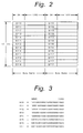
- a modulation signal modulated by RLL, (1, 7) is converted to the sector structure. That is, as shown in Fig. 2, the modulation signal is separated every 1092 channel bits and sync signals SY0 to SY7 each having 24 channel bits are inserted therebetween.
- the sync signal and the subsequent 1092 channel bits are called one sync frame.
- the sync signal SY0 is added only to the head sync frame of the sector.
- Fig. 2 shows the number of channel bits after the modulation.
- bit patterns of the sync signals SY0 to SY7 is shown in Fig. 3.
- (x) denotes that any one of '0' and '1' can be used.
- those are bit patterns which are not generated by the modulation of RLL (1, 7). Since accuracy of a signal demodulation is requested, the sync signal needs to be strong against an error as compared with the other signals.
- the bit patterns of the sync signals shown in Fig. 3 are selected so as to obtain good error resistive characteristics.
- RLL (1, 7) although a signal having an inversion interval of 2T to 8T can exist as mentioned above, in case of the reproduction signal from the disk, since a reproduction signal amplitude of a signal having a high frequency is not sufficiently large due to characteristics of the optical system, an error easily occurs in a signal of 2T having the highest frequency. It is prevented that an inversion interval of 2T exists in the sync signals SY0 to SY7, thereby making it different to cause an error.
- the sync signals SY0 to SY7 include the signal of 9T which does not exist in the RLL (1, 7) modulation signal and the inversion intervals of 9T are aligned between the sync signals.
- the reproduction signal can be again synchronized at '1' of 9T.
- a set of the sync signals SY0 to SY4 added to the sync frame on the left side of the diagram includes four '1' and a set of the sync signals SYS to SY7 added to the sync frame on the right side includes five '1'.
- the sync signal has a length of 24 channel bits. When the length is converted to the data length before modulation, it has a value which is integer times as long as two bytes. Consequently, a construction of the modulating/demodulating circuit can be set to a processing construction of a byte unit.
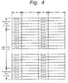
- One cluster is constructed by the above-mentioned 16 sectors, a preamble, and a postamble.
- One cluster is a data unit of recording/reproduction (rewriting).
- Fig. 4 shows a structure of one cluster.
- a cluster after bits for DSV control were added is called a cluster (2) and a cluster (Fig. 4) which does not include the bits for DSV control is called a cluster (1).
- the sync signals of the preamble start from SY4 and sequentially change like SY3, SY2, and SY1.
- the sync signal of the post amble is always SY4.
- Known predetermined data is inserted into the preamble and the postamble and is subjected to the modulating process in a manner similar to the data field.
- DSV Digital Sum Value
- the DSV is a value in which the bit of '1' is set to +1 and the bit of '0' is set to -1.
- DSV bits To converge the DSV obtained by accumulating the bit streams of the modulated data to 0 or a value close to 0 is a function of the DSV control bits (called DSV bits).
- the DSV bits are inserted into the modulated data stream on a 3-bit unit basis.
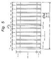
- Fig. 5 shows a structure of the cluster (2) in which the DSV bits were added to the above-mentioned one cluster (1).
- hatched regions show the inserted DSV bits.
- the DSV bits (three bits) are inserted to the modulated data of each line at predetermined intervals.
- One line includes two sync frames (two sync signals). It is unpreferable that the pattern of the sync signal changes as a result of the insertion of the DSV bits.
- the DSV bits (three bits) are inserted just after the first sync signal of each line. Subsequently, the DSV bits (three bits) are inserted after an interval of 186 channel bits.
- This method is repeated and the DSV bits (three bits) are sequentially inserted at total 12 places of the respective lines. Consequently, the DSV bits are positioned not only just after the first sync signal of each line but also just after the second sync signal.
- the demodulating process is executed. Since a deviation of synchronization is small just after the sync signal, the DSV bits can be certainly eliminated.
- a length of 189 bits constructed by the DSV bits of three bits and the data of 186 bits is called a DSV unit.
- the last 165 bits are used to construct a DSV unit together with a sync signal (24 channel bits) at the head of the next line.
- a channel bit frequency corresponding to the above-mentioned size of the cluster (2) is well matched with the frequency of a clock signal which is necessary for a reproducing process of a physical address.
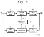
- Fig. 6 shows a construction which is included in the modulating unit 9 and is used to insert the DSV bits.
- the input data modulated by RLL (1, 7) is supplied to a 1DSV unit (189 channel bits) delay 21 and a DSV counter 24.
- An output of the 1DSV unit delay 21 is supplied to a DSV bit adding circuit 22.
- An output of the adding circuit 22 is supplied to an NRZI converting circuit 23.
- Output data including the DSV bits is extracted from the NRZI converting circuit 23.
- the NRZI converting circuit 23 Inverts the output signal.
- the circuit 23 doesn't invert the output signal.
- Output data of the NRZI converting circuit 23 is recorded on the disk.
- the output data is supplied to a DSV counter 25.
- a reset signal is supplied to the DSV counter 25.
- a resetting operation is executed only in the preamble field of the cluster (2). In the other fields, the resetting operation is not executed but the DSVs are successively accumulated. In case of recording data for the continuous clusters, it is sufficient to execute the resetting operation once at the start of the recording. In case of the continuous recording, the resetting operation is unnecessary.
- the DSV counter 25 executes the counting operation of '+1'.
- the counter executes the counting operation of '-1'.
- the DSV counter 24 to which the input data is supplied also executes the counting operation similar to that of the DSV counter 25 every 1DSV unit.
- the DSV counter 24 generates an accumulation value of the DSV of the 1DSV unit of the input data. Since the 1DSV unit delay 21 is provided, the DSV counter 25 generates an accumulation value of the DSVs of the output data up to the one-preceding DSV unit. Those accumulation values of the DSVs are compared by a comparator 26. A DSV polarity selecting circuit 27 is controlled by a comparison result of the comparator 26. A polarity selection signal of one bit for instructing a polarity of the DSV to be added is generated from the DSV polarity selecting circuit 27.
- '0' of the polarity selection signal indicates a case where '1' of the number of 0 or 2 should be included in the DSV bits of 3 bits (namely, the modulation waveform is not inverted).
- '1' of the polarity selection signal indicates a case where one '1' should be included in the DSV bits (namely, the modulation waveform is inverted).
- the DSV bit adding circuit 22 adds the DSV bits.
- Figs. 7 and 8 show tables of a conversion rule of the addition of the DSV bits which is performed in the DSV bit adding circuit 22.
- Fig. 7 shows the table when the polarity selection signal is equal to '0'.
- Fig. 8 shows the table when the polarity selection signal is equal to '1'.
- 2T to 8T denote inverting intervals of the position where the DSV bits of the input data modulated by RLL (1, 7) are inserted.
- Three bits shown by "ABC” denote the DSV bits which are actually inserted.
- "x" denotes that any one of '0' and '1' can be used.
- "*" in Fig. 7 denotes a case where the DSV cannot be controlled.
- As patterns of 3 bits in the DSV bits (000), (001), (010), (100), and (101) are used.
- the physical addresses which have previously been formed on the disk will now be described.
- guide grooves for tracking control have previously been formed on the disk.
- the guide grooves have been wobbled by a sine wave signal of a predetermined frequency (for example, 84.672 kHz) for controlling the rotation of the spindle motor.
- a carrier signal of such a frequency is frequency modulated by address information, thereby recording the address information to the guide grooves.
- the address information which is recorded by such a method is called an ADIP (ADdress In Pre-groove).
- the address starts from 0000h (h denotes a hexadecimal notation) and monotonously increases in the information area of the disk.
- Fig. 9 shows a construction of one sector (ADIP sector) of ADIP.
- the sector comprises: a sync signal of 4 bits; a cluster address (cluster H) of 8 bits; a cluster address (cluster M) of 8 bits; a cluster address (cluster L) of 4 bits; a sector address of 4 bits; and a CRC code for error detection of the cluster addresses and sector address.
- the cluster H, cluster M, and cluster L denote upper, middle, and lower addresses of the cluster addresses. Bit positions of (01) to (42) are specified for 42 bits of one sector shown in Fig. 9.
- Figs. 10A and 10B show an example and another example of the sync signal.
- the sync signal has a pattern of 8 channel bits of (11101000) and data which was bi-phase modulated subsequently follows.
- the data is obtained in a manner such that '0' of the data bit is converted to 2 bits serving as channel bits of (00) or (11) and '1' is converted to 2 bits serving as channel bits of (01).
- the pattern of the sync signal in Fig. 10A is used when the channel bit just before the sync signal is equal to '0'.
- the sync signal of a pattern of (00010111) is used.
- the bi-phase modulated ADIP data is analog frequency modulated.
- Fig. 11 shows an example of an encoder which is used when the wobbling grooves are previously formed on the disk.
- reference numeral 31 denotes a stable oscillator such as a crystal oscillator or the like.
- the oscillator 31 generates a signal of 169.344 kHz.
- An output of the oscillator 31 is supplied to a 1/2 frequency divider 32.
- a carrier signal of 84.672 kHz is generated in its output.
- the carrier signal is a wobbling frequency of the grooves which are spirally formed on the disk.
- the carrier signal is supplied to an FM modulator 33.
- the ADIP data having the sector structure shown in Fig. 9 is supplied to a bi-phase modulator 34.
- a bi-phase clock of 24.192 kHz obtained by frequency dividing the output of the oscillator 31 by a frequency divider 35 is supplied to the modulator 34.
- the bi-phase clock is a clock to read out each bit of the channel bits shown in Figs. 10A and 10B.
- the bi-phase modulator 34 executes processes for adding and modulating the sync signal and generates the bi-phase signal as shown in Figs. 10A and 10B.
- the bi-phase signal is supplied to the FM modulator 33 and is analog frequency modulated by using the carrier signal (84.672 kHz) from the frequency divider 32.
- the frequency modulation is performed in a manner such that, for example, when the data bit is equal to '0', a frequency deviation of -10% of the carrier frequency is caused and, when the data bit indicates '1', a frequency deviation of +10% of the carrier frequency is caused. Therefore, an average frequency of the FM modulation output is the carrier frequency (84.672 kHz).
- the guide grooves are formed on the disk by an output signal of the FM modulator 33.
- the carrier frequency (84.672 kHz), the construction of the ADIP sector, and the sector frequency (288 Hz) when the ADIP data is recorded to the wobbling grooves indicate values in case of a data transfer speed at which 18 clusters (2) are recorded or reproduced for one second.
- the construction is provided in the servo circuit 13 in the whole construction shown in Fig. 1.
- the reproduction signal A25 from the optical system 4 is supplied to an address component extracting unit 41.
- the extracting unit 41 is constructed by a band pass filter for separating a signal component mainly having the carrier frequency (84.672 kHz).
- the address component from the extracting unit 41 is supplied to an F/V converter 42.
- the F/V converter 42 generates an output voltage according to the frequency of the input signal.
- An output signal of the F/V converter 42 is supplied to a low pass filter 43.
- the low pass filter 43 eliminates unnecessary signal components.
- An FM demodulation signal is generated from the low pass filter 43.
- An output signal of the low pass filter 43 is supplied to a comparator 44 and is compared with a predetermined threshold value. As an output of the comparator 44, a binary signal, namely, bi-phase modulated ADIP data is outputted.
- the ADIP data is outputted as a reproduction address.
- the ADIP data from the comparator 44 is supplied to a phase comparator 45.
- a phase of the ADIP data is compared with that of an output of a VCO (voltage controlled oscillator) 47 by the phase comparator 45.
- An output signal of the phase comparator 45 is supplied as a control voltage to the VCO 47 via a filter 46.
- the filter 46 is a loop filter (low pass filter).
- a PLL is constructed by the phase comparator 45, filter 46, and VCO 47.
- a clock (24.192 kHz) of the bi-phase modulation synchronized with the ADIP data is outputted from the VCO 47.
- the clock is used to read the reproduction ADIP data outputted from the comparator 44 by sampling. That is, the ADIP data and read clock are supplied to a data decoding unit (not shown). '1' and '0' of the data are discriminated at a timing of the read clock by the data decoding unit.
- the modulating unit 9 is constructed by an encoding processing unit 51 and a modulating unit 52.
- the encoding processing unit 51 executes the processes for setting the data to be recorded to the sector structure including the sync signal, constructing the cluster (1) from a plurality of sectors, and constructing the cluster (2) by adding the DSV bits to the cluster (1).
- the modulating unit 52 performs the modulation of RLL (1, 7).
- the above-mentioned physical address reproduction processing unit constructed by the FM demodulating unit and PLL is shown by reference numeral 40 in Fig. 13.
- an oscillator 53 which is constructed by a crystal oscillator or the like and has an oscillating frequency of 17.635968 MHz is provided as an original oscillator.
- a frequency of an output signal of the oscillator 53 is divided by a 1/2 frequency divider 54.
- the clock signal of 8.81798 MHz can be obtained from the 1/2 frequency divider 54.
- the clock signal is used for the signal process in the encoding processing unit 51 and modulating unit 52 of the modulating unit 9.
- an output of the oscillator 53 is used for the signal process in the physical address processing unit 40.
- the frequency is the same as that of the read clock generated by the physical address reproduction processing unit 40.
- the above-mentioned frequency relation means that the clock signal which is necessary for both of them can be generated by simple hardware. In other words, if one clock is prepared as an original oscillation, the process for the signal to be recorded to the disk and the reproducing process of the physical address data previously formed on the disk can be simultaneously executed by using such a clock.
- a construction of a conventional optical disk apparatus [specifically speaking, a mini disc (MD)] is shown in Fig. 14.
- reference numeral 90 denotes a modulating unit for forming a recording signal to the mini disc and 100 indicates a physical address reproduction processing unit for frequency demodulating a reproduction RF signal, generating ADIP data, and generating a clock to read the ADIP data by the PLL.
- the modulating unit 90 and physical address reproduction processing unit 100 are similar to those in the embodiment of the invention.
- an EFM modulation is used in the mini disc.
- reference numeral 61 denotes an oscillator as an original oscillation.
- a frequency of an output of the oscillator 61 is equal to 22.57792 MHz.
- the output of the oscillator 61 is used as a clock for processing in the physical address reproduction processing unit 100.
- the clock frequency necessary for the modulating unit 90 is equal to 4.3218 MHz (channel bit frequency) in consideration of a cluster size, a modulating system, and the like. Since the relation between those frequencies is not an integer ratio, the clock of the frequency necessary for the modulating unit 90 is formed by the PLL.
- the PLL is constructed by a VCO 62 having a center of 4.3218 MHz, frequency dividers 63 and 64, and a phase comparator 65.
- the VCO 62 generates a clock signal of a frequency of 4.3218 MHz which is necessary for the process of the modulating unit 90.
- a frequency of an output of the VCO 62 is divided into 1/49 by the frequency divider 64 and is set to a signal of a frequency of 88.2 kHz.
- An output of the frequency divider 64 is supplied as one input signal of the phase comparator 65.
- phase comparator 65 As another input signal of the phase comparator 65, a signal of a frequency of 88.2 kHz obtained by dividing a frequency (22.5792 MHz) of an output signal of the oscillator 61 into 1/256 is supplied. Therefore, the VCO 62 of the PLL generates a clock signal of 4.3218 MHz synchronized with the output signal of the oscillator 61.
- the necessary first and second clock signals can be formed by a simple construction comprising the oscillator 53 and 1/2 frequency divider 54 (constructed by a flip-flop).
- problems such as increase in electronic power consumption, high frequency noise interference to the outside, instability or the like due to an aging change and a temperature change, and the like occur. In the invention, the above problems do not occur.
- the invention can be also applied to a recordable optical disk, for example, an optical disk of a phase-change type besides the magnetooptic disk.
- the relation between the frequency of the first clock signal necessary for the physical address processing unit and the frequency of the second clock signal necessary for the modulating unit can be set to the integer ratio. Consequently, the necessary first and second clock signals can be formed by the simple construction comprising the common oscillator and frequency divider.
Applications Claiming Priority (3)
| Application Number | Priority Date | Filing Date | Title |
|---|---|---|---|
| JP14222297 | 1997-05-30 | ||
| JP142222/97 | 1997-05-30 | ||
| JP9142222A JPH10334616A (ja) | 1997-05-30 | 1997-05-30 | 光ディスク装置およびデータ記録方法 |
Publications (2)
| Publication Number | Publication Date |
|---|---|
| EP0881641A2 true EP0881641A2 (fr) | 1998-12-02 |
| EP0881641A3 EP0881641A3 (fr) | 2001-08-22 |
Family
ID=15310263
Family Applications (1)
| Application Number | Title | Priority Date | Filing Date |
|---|---|---|---|
| EP98303843A Withdrawn EP0881641A3 (fr) | 1997-05-30 | 1998-05-15 | Appareil de disques optique et méthode d'enregistrement de données |
Country Status (4)
| Country | Link |
|---|---|
| US (1) | US6072756A (fr) |
| EP (1) | EP0881641A3 (fr) |
| JP (1) | JPH10334616A (fr) |
| KR (1) | KR19980087563A (fr) |
Cited By (2)
| Publication number | Priority date | Publication date | Assignee | Title |
|---|---|---|---|---|
| EP1020859A1 (fr) * | 1999-01-14 | 2000-07-19 | Hewlett-Packard Company | Support d'enregistrement optique |
| EP1455456A1 (fr) * | 2001-12-11 | 2004-09-08 | Sony Corporation | Appareil et procede de modulation et procede de production de bits de commande de dsv |
Families Citing this family (14)
| Publication number | Priority date | Publication date | Assignee | Title |
|---|---|---|---|---|
| JPH11120560A (ja) * | 1997-10-17 | 1999-04-30 | Sony Corp | 光ディスクの記録方法及びアクセス方法、光ディスク、光ディスク記録装置及び光ディスク装置 |
| JP3985173B2 (ja) * | 1998-05-29 | 2007-10-03 | ソニー株式会社 | 変調装置および方法、復調装置および方法、並びにデータ格納媒体 |
| KR100424482B1 (ko) * | 2000-06-22 | 2004-03-24 | 엘지전자 주식회사 | 일련의 데이터 워드를 변조신호로 변환하는 방법 및 장치 |
| CN100353447C (zh) * | 2000-12-26 | 2007-12-05 | 松下电器产业株式会社 | 记录方法、再现方法、记录装置和再现装置 |
| JP2003085898A (ja) * | 2001-09-12 | 2003-03-20 | Toshiba Corp | 情報記憶媒体、情報記録装置、情報記録方法、情報再生装置、及び情報再生装置 |
| KR100513327B1 (ko) * | 2001-12-21 | 2005-09-07 | 엘지전자 주식회사 | 광디스크 워블신호의 변조장치/방법 및 복조장치/방법 |
| JP3514255B2 (ja) * | 2002-01-10 | 2004-03-31 | 日本電気株式会社 | Vco回路、pll回路、及び、情報記録装置 |
| JP4178795B2 (ja) * | 2002-01-23 | 2008-11-12 | ソニー株式会社 | 変調装置および方法、dsv制御ビット生成方法、記録媒体、並びにプログラム |
| JP3993818B2 (ja) * | 2002-12-16 | 2007-10-17 | 松下電器産業株式会社 | 再生信号処理装置 |
| JP4826888B2 (ja) * | 2005-11-10 | 2011-11-30 | ソニー株式会社 | 復調テーブル、復調装置および復調方法、プログラム、並びに記録媒体 |
| JP4839784B2 (ja) * | 2005-11-10 | 2011-12-21 | ソニー株式会社 | 変調テーブル、変調装置および方法、プログラム、並びに記録媒体 |
| JP4692234B2 (ja) * | 2005-11-10 | 2011-06-01 | ソニー株式会社 | 変調テーブル、変調装置および方法、プログラム、並びに記録媒体 |
| KR20090085257A (ko) * | 2008-02-04 | 2009-08-07 | 삼성전자주식회사 | Dsv 제어 방법, 이에 적합한 기록매체 및 장치 |
| US8958276B1 (en) | 2012-10-31 | 2015-02-17 | Marvell International Ltd. | Optical disc drive high frequency modulation signal detection |
Citations (3)
| Publication number | Priority date | Publication date | Assignee | Title |
|---|---|---|---|---|
| EP0485234A2 (fr) * | 1990-11-09 | 1992-05-13 | Sharp Kabushiki Kaisha | Appareil pour l'enregistrement et la reproduction d'information |
| EP0597443A1 (fr) * | 1992-11-09 | 1994-05-18 | Sony Corporation | Méthode de modulation, dispositif de modulation et dispositif de démodulation |
| EP0758125A2 (fr) * | 1995-08-09 | 1997-02-12 | Sony Corporation | Milieu d'enregistrement, appareil d'enregistrement et appareil de lecture |
Family Cites Families (1)
| Publication number | Priority date | Publication date | Assignee | Title |
|---|---|---|---|---|
| JPH0969230A (ja) * | 1995-08-31 | 1997-03-11 | Sony Corp | 光ディスク、光ディスク記録再生装置および方法 |
-
1997
- 1997-05-30 JP JP9142222A patent/JPH10334616A/ja not_active Abandoned
-
1998
- 1998-05-13 US US09/078,234 patent/US6072756A/en not_active Expired - Fee Related
- 1998-05-15 EP EP98303843A patent/EP0881641A3/fr not_active Withdrawn
- 1998-05-30 KR KR1019980020753A patent/KR19980087563A/ko not_active Application Discontinuation
Patent Citations (3)
| Publication number | Priority date | Publication date | Assignee | Title |
|---|---|---|---|---|
| EP0485234A2 (fr) * | 1990-11-09 | 1992-05-13 | Sharp Kabushiki Kaisha | Appareil pour l'enregistrement et la reproduction d'information |
| EP0597443A1 (fr) * | 1992-11-09 | 1994-05-18 | Sony Corporation | Méthode de modulation, dispositif de modulation et dispositif de démodulation |
| EP0758125A2 (fr) * | 1995-08-09 | 1997-02-12 | Sony Corporation | Milieu d'enregistrement, appareil d'enregistrement et appareil de lecture |
Cited By (4)
| Publication number | Priority date | Publication date | Assignee | Title |
|---|---|---|---|---|
| EP1020859A1 (fr) * | 1999-01-14 | 2000-07-19 | Hewlett-Packard Company | Support d'enregistrement optique |
| US6501721B2 (en) | 1999-01-14 | 2002-12-31 | Hewlett-Packard Company | Spliceless editing of a read/write optical medium |
| EP1455456A1 (fr) * | 2001-12-11 | 2004-09-08 | Sony Corporation | Appareil et procede de modulation et procede de production de bits de commande de dsv |
| EP1455456A4 (fr) * | 2001-12-11 | 2007-05-23 | Sony Corp | Appareil et procede de modulation et procede de production de bits de commande de dsv |
Also Published As
| Publication number | Publication date |
|---|---|
| EP0881641A3 (fr) | 2001-08-22 |
| JPH10334616A (ja) | 1998-12-18 |
| US6072756A (en) | 2000-06-06 |
| KR19980087563A (ko) | 1998-12-05 |
Similar Documents
| Publication | Publication Date | Title |
|---|---|---|
| US6072756A (en) | Optical disk apparatus and data recording method | |
| US5815486A (en) | Optical disk, recording/reproducing apparatus and method for rapidly recording/reproducing data on/from an optical disk using gray coding | |
| KR100983991B1 (ko) | 주파수 및 위상 제어 장치와 최대 우도 디코더 | |
| EP0813198B1 (fr) | Appareil et méthode d'enregistrement et de reproduction et disque associé | |
| US8014241B2 (en) | Information recording method and apparatus | |
| JP3850600B2 (ja) | 情報記録ディスクおよび情報記録装置 | |
| US6201778B1 (en) | Optical disk with a groove for defining serial data modulated into a signal using phase and frequency modulation | |
| US5093820A (en) | Optical disk recording/reproducing device | |
| US5604727A (en) | Data recording medium an optical disk and an optical disk apparatus | |
| US5689488A (en) | Optical disc system, optical disc and recording method | |
| US5864531A (en) | DC level fluctuation correction by selecting a time constant coupled to a reproduced signal | |
| US6665246B2 (en) | Optical disk apparatus | |
| JPH0817144A (ja) | データ変調装置およびデータ復調装置 | |
| JP3004106U (ja) | ディスク媒体及びその記録再生装置 | |
| KR100801037B1 (ko) | 정보 기록방법, 정보 기록장치 및 정보 기록매체 | |
| JP3456619B2 (ja) | ディスク、ディスク形成装置、ディスク形成方法、ディスク記録再生装置、およびディスク記録再生方法 | |
| KR100413683B1 (ko) | 워블신호가 기록된 광 기록매체, 그 워블신호 기록장치 및기록방법 | |
| JPH10312639A (ja) | 光ディスクの製造方法、光ディスク及び光ディスク装置 | |
| KR100195555B1 (ko) | 기록 장치 및 재생장치 | |
| JP2002092874A (ja) | ビットアキュレートな光学ドライブにおける位相不連続性の補償 | |
| JP2001143407A (ja) | アドレス検出回路およびアドレス検出回路を備えた記録および/または再生装置 | |
| JPH08249830A (ja) | ディスク媒体記録再生方法およびクロック信号発生装置 | |
| JPH05189884A (ja) | データ同期化装置 | |
| JPH02156476A (ja) | ディスク記憶装置用ディジタル再生方法及び装置 | |
| JP2001093202A (ja) | パルスレーザ制御回路およびパルスレーザ制御回路を備えた記録再生装置 |
Legal Events
| Date | Code | Title | Description |
|---|---|---|---|
| PUAI | Public reference made under article 153(3) epc to a published international application that has entered the european phase |
Free format text: ORIGINAL CODE: 0009012 |
|
| AK | Designated contracting states |
Kind code of ref document: A2 Designated state(s): AT BE CH CY DE DK ES FI FR GB GR IE IT LI LU MC NL PT SE |
|
| AX | Request for extension of the european patent |
Free format text: AL;LT;LV;MK;RO;SI |
|
| PUAL | Search report despatched |
Free format text: ORIGINAL CODE: 0009013 |
|
| AK | Designated contracting states |
Kind code of ref document: A3 Designated state(s): AT BE CH CY DE DK ES FI FR GB GR IE IT LI LU MC NL PT SE |
|
| AX | Request for extension of the european patent |
Free format text: AL;LT;LV;MK;RO;SI |
|
| 17P | Request for examination filed |
Effective date: 20020128 |
|
| AKX | Designation fees paid |
Free format text: DE FR GB |
|
| 17Q | First examination report despatched |
Effective date: 20020517 |
|
| STAA | Information on the status of an ep patent application or granted ep patent |
Free format text: STATUS: THE APPLICATION IS DEEMED TO BE WITHDRAWN |
|
| 18D | Application deemed to be withdrawn |
Effective date: 20100914 |