EP0878863B1 - Mobile communication apparatus - Google Patents
Mobile communication apparatus Download PDFInfo
- Publication number
- EP0878863B1 EP0878863B1 EP98108641A EP98108641A EP0878863B1 EP 0878863 B1 EP0878863 B1 EP 0878863B1 EP 98108641 A EP98108641 A EP 98108641A EP 98108641 A EP98108641 A EP 98108641A EP 0878863 B1 EP0878863 B1 EP 0878863B1
- Authority
- EP
- European Patent Office
- Prior art keywords
- circuit board
- chip antenna
- reflecting plate
- substrate
- major surface
- Prior art date
- Legal status (The legal status is an assumption and is not a legal conclusion. Google has not performed a legal analysis and makes no representation as to the accuracy of the status listed.)
- Expired - Lifetime
Links
Images


Classifications
-
- H—ELECTRICITY
- H01—ELECTRIC ELEMENTS
- H01Q—ANTENNAS, i.e. RADIO AERIALS
- H01Q1/00—Details of, or arrangements associated with, antennas
- H01Q1/12—Supports; Mounting means
- H01Q1/22—Supports; Mounting means by structural association with other equipment or articles
- H01Q1/24—Supports; Mounting means by structural association with other equipment or articles with receiving set
-
- H—ELECTRICITY
- H01—ELECTRIC ELEMENTS
- H01Q—ANTENNAS, i.e. RADIO AERIALS
- H01Q1/00—Details of, or arrangements associated with, antennas
- H01Q1/36—Structural form of radiating elements, e.g. cone, spiral, umbrella; Particular materials used therewith
- H01Q1/38—Structural form of radiating elements, e.g. cone, spiral, umbrella; Particular materials used therewith formed by a conductive layer on an insulating support
-
- H—ELECTRICITY
- H01—ELECTRIC ELEMENTS
- H01Q—ANTENNAS, i.e. RADIO AERIALS
- H01Q19/00—Combinations of primary active antenna elements and units with secondary devices, e.g. with quasi-optical devices, for giving the antenna a desired directional characteristic
- H01Q19/10—Combinations of primary active antenna elements and units with secondary devices, e.g. with quasi-optical devices, for giving the antenna a desired directional characteristic using reflecting surfaces
Definitions
- the present invention relates to mobile communication apparatuses having a built-in type chip antenna for use in mobile communications and local area networks.
- a known mobile communication apparatus for example, a mobile cellular telephone 50, is formed, as shown in Fig. 10, by disposing a circuit board 53 within a case 54.
- the circuit board 53 is configured in such a manner that a non-directional chip antenna 51 is mounted on one major surface (first major surface) 53a and a ground pattern 52 is provided on the other major surface (second major surface) 53b. Radio waves are received by the chip antenna 51.
- the chip antenna 51 is electrically connected via a transmission line (not shown) on the circuit board 53 to an RF portion 55 of the cellular telephone 50 disposed on the second major surface 53b.
- the bandwidth of the chip antenna 51 is determined by the stray capacitance generated between the chip antenna 51 and the ground pattern 52 provided on the second major surface 53b of the circuit board 53.
- the chip antenna has non-directional characteristics, transmitting radio waves are influenced by a user holding the telephone while using it, thereby deteriorating the antenna characteristics.
- the ground pattern is provided on the second major surface of the circuit board opposite to the first major surface on which the chip antenna is mounted.
- the stray capacitance generated between the chip antenna and the ground pattern provided on the second major surface of the circuit board should be increased. This disadvantageously enlarges the ground pattern, and inevitably also increases the size of the circuit board, resulting in an enlargement of the cellular telephone.
- the RF portion of the cellular telephone is mounted on the first major surface of the circuit board, thereby restricting the position at which the ground pattern is formed on the first major surface of the circuit board.
- the present invention provides a mobile communication apparatus, comprising: a circuit board having a ground pattern thereon; a non-directional chip antenna mounted on the circuit board; and a case housing the circuit board and the non-directional chip antenna; wherein a reflecting plate is provided between a first major surface of the circuit board and the case with a space between the reflecting plate and the circuit board and said reflecting plate (14) is electrically connected to the ground pattern on the circuit board.
- the chip antenna may be mounted on the first or second major surface of said circuit board.
- the chip antenna may comprise a substrate made of at least one of a dielectric material and a magnetic material, at least one conductor provided at least on a surface of the substrate and within the substrate, and at least one feeding terminal provided on a surface of the substrate in order to apply a voltage to the conductor.
- a circuit board is configured in such a manner that a chip antenna is mounted on a first or second major surface and a ground pattern is provided on the first major surface.
- a reflecting plate is electrically connected to the ground pattern on the circuit board.
- the first major surface of the circuit board and the reflecting plate are placed to face each other with an intervening gap therebetween.
- the reflecting plate which is electrically connected to the ground pattern on the circuit board, is provided between the circuit board and a frame portion, which forms a case within which the non-directional chip antenna is stored. Consequently, due to the reflection effect of the reflecting plate, the transmission output of the chip antenna is reliably reflected in the direction opposite to the direction in which the reflecting plate is disposed. This makes it possible to provide a mobile communication apparatus with a directivity in a specific direction.
- a reflecting plate is provided on the side of the user holding the cellular telephone, thereby reducing the influence of the user, which would otherwise cause a decrease in the antenna characteristics during the transmitting and receiving operation.
- the chip antenna has a rectangular-prism-shaped substrate essentially consisting of barium oxide, aluminum oxide, and silica, the propagation speed is decreased, which further causes a shortened wavelength. Accordingly, when the relative dielectric constant of the substrate is indicated by ⁇ , the effective line length is increased by ⁇ 1/2 , which is longer than the effective line length of a known linear antenna. Thus, the current is distributed over a wider area, and accordingly, the amount of radiating waves is increased, there enhancing the gain of the chip antenna. In other words, if the gain of a chip antenna is the same as that of a known antenna, the chip antenna can be miniaturized. As a result, a cellular telephone having the miniaturized chip antenna is accordingly downsized.
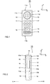
- Fig. 1 is a front view, partially perspective, illustrating a mobile cellular telephone according to a first embodiment of a mobile communication apparatus of the present invention.
- Fig. 2 is a side view, partially perspective, illustrating the mobile communication apparatus shown in Fig. 1.
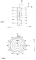
- Fig. 3 is a perspective view illustrating a chip antenna usable for the mobile communication apparatus shown in Fig. 1.
- Fig. 4 is an exploded perspective view illustrating the chip antenna shown in Fig. 3.
- Fig. 5 is a perspective view illustrating an example of modifications made to the chip antenna shown in Fig. 3.
- Fig. 6 is a perspective view illustrating another example of modifications made to the chip antenna shown in Fig. 3.
- Fig. 7 is a side view, partially perspective, illustrating a mobile cellular telephone according to a second embodiment of a mobile communication apparatus of the present invention.
- Fig. 8 illustrates the antenna gain when the user does not approach from the direction A.
- Fig. 9 illustrates the antenna gain when the user approaches from the direction A.
- Fig. 10 is a side view, partially perspective, illustrating a mobile cellular telephone, which serves as a prior art mobile communication apparatus.
- a mobile communication apparatus for example, a mobile cellular telephone, is described below with reference to the drawings.
- Figs. 1 and 2 are respectively a front view and a side view, both of which are partially perspective, of a first embodiment of a mobile communication apparatus according to the present invention.
- a mobile cellular telephone 10 comprises a case 11, which has frame portions 11a through 11f made of, for example, a reinforced plastic, a non-directional chip antenna 12, a circuit board 13 having the chip antenna 12 on one major surface (first major surface) 13a, and a copper-made reflecting plate 14, which serves as means for attenuating a transmission output of the chip antenna 12.
- the frame portion 11e which forms the case 11, has a telephone receiver 15, a telephone transmitter 16, and dial keys 17. Moreover, the chip antenna 12 is electrically connected via a transmission line (not shown) on the circuit board 13 to an RF portion 18 of the cellular telephone 10 disposed on the first major surface 13a of the circuit board 13.
- the reflecting plate 14 is disposed between the circuit board 13 and the frame portion 11e in such a manner that it faces the first major surface 13a with an intervening gap. Also, the reflecting plate 14 is connected to a ground pattern 19 provided on the first major surface 13a of the circuit board 13 via a short-circuit plate 14a.
- the circuit board 13 and the reflecting plate 14, which is connected to the ground pattern 19 on the first major surface 13a of the circuit board 13, are placed to face each other with a gap therebetween.
- the reflecting plate 14 is required to be enlarged to increase the capacitance between the chip antenna 12 and the ground pattern 19 on the first major surface 13a of the circuit board 13 without needing to increase the size of the circuit board 13. This makes it possible to reduce the size and to increase the bandwidth of the cellular telephone 10.
- the chip antenna 12 has a conductor 2, as illustrated in Figs. 3 and 4, disposed within a rectangular-prism-shaped substrate 1 in such a manner that the conductor 2 is spirally wound in the longitudinal direction of the substrate 1.
- the substrate 1 is formed by laminating rectangular sheet layers 3a through 3c, which are made of a dielectric material essentially consisting of barium oxide, aluminum oxide, and silica.
- conductive patterns 4a through 4h are substantially linear or formed substantially in an L shape, and formed of copper or a copper alloy.
- the sheet layers 3a through 3c are then laminated and sintered, and the conductive patterns 4a through 4h are connected through the via-holes 5, thereby forming the conductor 2 spirally wound within the substrate 1 in the longitudinal direction of the substrate 1.
- One end of the conductor 2 (one end of the conductive pattern 4a) is led to an end face of the substrate 1 and is connected to a feeding terminal 6 which is provided over the surfaces of the substrate 1 and which is used for applying a voltage to the conductor 2.
- the other end of the conductor 2 (one end of the conductive pattern 4h) forms a free end 7 within the substrate 1.
- FIGs. 5 and 6 are perspective views of examples of modifications made to the chip antenna 12 shown in Fig. 3.
- a chip antenna 12a illustrated in Fig. 5 has a rectangular-prism-shaped substrate 1a, a conductor 2a spirally wound along the surfaces of the substrate 1a in the longitudinal direction of the substrate 1a, and a feeding terminal 6a provided over the surfaces of the substrate 1a and used for applying a voltage to the conductor 2a.
- one end of the conductor 2a is connected on the surface of the substrate 1a to the feeding terminal 6a, while the other end of the conductor 2a forms a free end 7a on the surface of the substrate 1a.
- the conductor 2a can be easily formed spirally on the surfaces of the substrate 1a by means such as screen printing, thereby simplifying the manufacturing process of the chip antenna 12a.
- a chip antenna 12b illustrated in Fig. 6 has a rectangular-prism-shaped substrate 1b, a meandering conductor 2b formed on the surface (one major surface) of the substrate 1b, and a feeding terminal 6b provided over the surfaces of the substrate 1b and used for applying a voltage to the conductor 2b.
- one end of the conductor 2b is connected on the surface of the substrate 1b to the feeding terminal 6b, while the other end of the conductor 2b forms a free end 7b on the surface of the substrate 1b.
- the meandering conductor 2b since the meandering conductor 2b is formed only on one major surface of the substrate 1b, the height of the substrate 1b can be decreased, thereby accordingly reducing the height of the chip antenna 12b.
- the meandering conductor 2b may be formed within the substrate 1b.
- Fig. 7 is a side view, which is partially perspective, illustrating a second embodiment of a mobile communication apparatus according to the present invention.
- a mobile cellular telephone 20 differs from the cellular telephone 10 of the first embodiment in that the chip antenna 12 is mounted on the other major surface (second major surface) 13b of the circuit board 13.
- Fig. 8 illustrates the results obtained by comparing the antenna gain of the mobile cellular telephones 10 and 20 (Figs. 1 and 7) of the respective first and second embodiments with the antenna gain of a cellular telephone without a reflecting plate when a user did not approach from the direction A to hold the telephone.
- the solid lines indicate the antenna gain of the cellular telephones 10 and 20 of the respective first and second embodiments, while the broken line represents the antenna gain of the telephone without a reflecting plate.
- the directions x, y, and z and the directions A and B correspond to those shown in Figs. 2 and 7. Comparing the cellular telephones 10 and 20 of the respective first and second embodiments to the cellular telephone without a reflecting plate, Fig. 8 clearly reveals that the antenna gain on the side on which the reflecting plate is provided (the direction A) is decreased, and the antenna gain on the side opposite to the direction A (the direction B) is increased.
- Fig. 9 illustrates the results obtained by comparing the antenna gain of the cellular telephones 10 and 20 of the first and second embodiments (Figs. 1 and 7) with the antenna gain of the cellular telephone without a reflecting plate when the user approached from the direction A to take hold of the telephone.
- the solid lines indicate the antenna gain of the cellular telephones 10 and 20 of the respective first and second embodiments, while the broken line represents the antenna gain of the cellular telephone without a reflecting plate.
- the directions x, y, and z and the directions A and B correspond to those shown in Figs. 2 and 7.
- Fig. 9 indicates that the user approaching from the direction A to take hold of the telephone influences the antenna gain in the direction B, thereby lowering the antenna gain in the overall peripheral direction.
- the antenna gain in the direction B is hardly lowered, and therefore, there is no influence by the user approaching from the direction A to take hold of the telephone.
- the antenna gain is lowered if the user approaches to take hold of the cellular telephone. This is because the electromagnetic waves around the telephone are disturbed by the user.
- the transmitting radio waves are hardly output in the direction in which the reflecting plate is provided. Accordingly, electromagnetic waves are not disturbed even if the user approaches to take hold of the telephone.
- a circuit board is provided in such a manner that a chip antenna is mounted on a first or second major surface and a ground pattern is formed on the first major surface.
- a reflecting plate is connected to the ground pattern of the circuit board.
- the first major surface of the circuit board and the reflecting plate are placed to face each other with an intervening gap therebetween.
- the reflecting plate which is connected to the ground pattern on the circuit board, is provided between the circuit board and a frame portion, which forms a case for accommodating the non-directional chip therein. Consequently, due to the reflection effect of the reflecting plate, the transmission output of the chip antenna is reliably reflected in the direction opposite to the direction in which the reflecting plate is disposed. This makes it possible to provide a mobile communication apparatus with a directivity in a specific direction.
- a reflecting plate is provided on the side of the user holding the cellular telephone, thereby reducing the influence of the user, which would otherwise cause a decrease in the antenna characteristics during the transmitting and receiving operation.
- the chip antenna has a rectangular-prism-shaped substrate essentially consisting of barium oxide, aluminum oxide, and silica, the propagation speed is decreased, which further causes a shortened wavelength. Accordingly, when the relative dielectric constant of the substrate is indicated by ⁇ , the effective line length is increased by ⁇ 1/2 , which is longer than the effective line length of a known linear antenna. Thus, the current is distributed over a wider area, and accordingly, the amount of radiating waves is increased, thereby enhancing the gain of the chip antenna. In other words, if the gain of a chip antenna is set to that of a known antenna, the chip antenna can be miniaturized over the known antenna. As a result, a cellular telephone having the miniaturized chip antenna can be downsized.
- the substrate of the chip antenna is formed from a dielectric material essentially consisting of barium oxide, aluminum oxide, and silica.
- the substrate is not restricted to the above dielectric material, and may be a dielectric material essentially consisting of titanium oxide and neodymium oxide, a magnetic material essentially consisting of nickel, cobalt, and iron, or a combination of a dielectric material and a magnetic material.
- the chip antenna may have a plurality of resonant frequencies in accordance with the number of conductors, thereby making it possible to cope with multi-bands with only a single antenna.
- a conductor is formed within or on the surface of the substrate of the chip antenna. Conductors may be formed both within and on the surface of the substrate.
- the reflecting plate may be positioned at any portion as long as it is provided between the circuit board and the frame portion, which is positioned in the direction in which the transmission output of the non-directional chip antenna is reflected.
- a copper plate is used for the reflecting plate
- a conductor formed on a printed board or a ceramic board by means such as vapor-depositing or plating may be used for the reflecting plate.
- advantages similar to those exhibited by the use of the copper plate are offered.
- the reflecting plate is formed separately from the frame portion for forming the case.
- the reflecting plate may be formed of a sheet-like conductor directly laminated on the frame portion or a conductor formed by directly placing a vapor-deposited or plated film on the case. The reflecting plate may be then connected via a short-circuit plate to the ground pattern provided on the first major surface of the circuit board.
- the reflecting plate since the reflecting plate is directly laminated on the frame portion for forming the case, the thickness of the case can be reduced, thereby making the resulting mobile communication apparatus thinner.
Applications Claiming Priority (6)
| Application Number | Priority Date | Filing Date | Title |
|---|---|---|---|
| JP12421397 | 1997-05-14 | ||
| JP12421397 | 1997-05-14 | ||
| JP124213/97 | 1997-05-14 | ||
| JP10452898 | 1998-04-15 | ||
| JP10104528A JPH1131909A (ja) | 1997-05-14 | 1998-04-15 | 移動体通信機 |
| JP104528/98 | 1998-04-15 |
Publications (3)
| Publication Number | Publication Date |
|---|---|
| EP0878863A2 EP0878863A2 (en) | 1998-11-18 |
| EP0878863A3 EP0878863A3 (en) | 2000-02-23 |
| EP0878863B1 true EP0878863B1 (en) | 2004-09-15 |
Family
ID=26444983
Family Applications (1)
| Application Number | Title | Priority Date | Filing Date |
|---|---|---|---|
| EP98108641A Expired - Lifetime EP0878863B1 (en) | 1997-05-14 | 1998-05-12 | Mobile communication apparatus |
Country Status (4)
| Country | Link |
|---|---|
| US (1) | US6031731A (ja) |
| EP (1) | EP0878863B1 (ja) |
| JP (1) | JPH1131909A (ja) |
| DE (1) | DE69826174T2 (ja) |
Families Citing this family (24)
| Publication number | Priority date | Publication date | Assignee | Title |
|---|---|---|---|---|
| JP3838815B2 (ja) | 1999-05-10 | 2006-10-25 | 日本電気株式会社 | 携帯電話機 |
| WO2000072404A1 (fr) * | 1999-05-21 | 2000-11-30 | Matsushita Electric Industrial Co., Ltd. | Antenne de communication mobile et appareil de communication mobile dans lequel elle est utilisee |
| GB2350482A (en) * | 1999-05-27 | 2000-11-29 | Hugh Henry Andrew Pincherle | Mobile 'phone with antenna pointing away from user's head |
| SE515832C2 (sv) | 1999-12-16 | 2001-10-15 | Allgon Ab | Slitsantennanordning |
| DE10039427A1 (de) * | 2000-08-11 | 2002-02-21 | Siemens Ag | Antennenanordnung eines mobilen Kommunikationsendgerätes, insbesondere eines Mobiltelefons |
| JP3642029B2 (ja) | 2001-02-06 | 2005-04-27 | 日本電気株式会社 | 携帯電話機 |
| US6674405B2 (en) | 2001-02-15 | 2004-01-06 | Benq Corporation | Dual-band meandering-line antenna |
| US6774847B1 (en) * | 2001-03-01 | 2004-08-10 | Symbol Technologies, Inc. | System and method providing integrated chip antenna with display for communications devices |
| KR100416885B1 (ko) * | 2001-07-27 | 2004-02-05 | (주)신아정보통신 | 무선데이터 통신용 소형 안테나 |
| DE60201878T2 (de) * | 2002-01-28 | 2005-03-17 | Sony International (Europe) Gmbh | Mobilfunkgerät mit geerdetem Strahlungsabschirmungsrahmen |
| GB2390957B (en) * | 2002-07-15 | 2005-11-23 | * Motorola, Inc | System for enhanced radiation performance of a communication device |
| US7162264B2 (en) * | 2003-08-07 | 2007-01-09 | Sony Ericsson Mobile Communications Ab | Tunable parasitic resonators |
| US7274953B2 (en) * | 2003-10-07 | 2007-09-25 | Kabushiki Kaisha Fine Rubber Kenkyuusho | Portable telephone with reduced specific absorption rate and improved efficiency |
| US20060111162A1 (en) * | 2004-11-24 | 2006-05-25 | Samsung Electronics Co., Ltd. | Portable wireless terminal having conductor for improving antenna property |
| JP4413145B2 (ja) * | 2005-01-14 | 2010-02-10 | ソニー・エリクソン・モバイルコミュニケーションズ株式会社 | 携帯無線端末装置 |
| JP4565006B2 (ja) * | 2005-03-14 | 2010-10-20 | 株式会社小松製作所 | ブレードおよびこのブレードを備えたファン |
| US7629928B2 (en) * | 2005-03-23 | 2009-12-08 | Kyocera Wireless Corp. | Patch antenna with electromagnetic shield counterpoise |
| JP4102411B2 (ja) | 2006-04-13 | 2008-06-18 | 株式会社東芝 | 移動通信端末 |
| JP2008061109A (ja) * | 2006-09-01 | 2008-03-13 | Toshiba Corp | 電子機器および電気回路 |
| JP4814804B2 (ja) * | 2007-01-17 | 2011-11-16 | シャープ株式会社 | 移動体無線通信機 |
| US7554496B2 (en) | 2007-04-10 | 2009-06-30 | Research In Motion Limited | Mobile wireless communications device including a ground patch providing specific absorption rate (SAR) reduction and related methods |
| JP4649522B2 (ja) * | 2009-05-29 | 2011-03-09 | 株式会社東芝 | ノートブック型パーソナルコンピュータ |
| JP2011199494A (ja) | 2010-03-18 | 2011-10-06 | Panasonic Corp | アンテナ装置、およびそれを備えた電子機器 |
| KR20190060283A (ko) | 2017-11-24 | 2019-06-03 | 삼성전자주식회사 | 안테나를 포함하는 전자 장치 |
Citations (1)
| Publication number | Priority date | Publication date | Assignee | Title |
|---|---|---|---|---|
| EP0648023A1 (en) * | 1993-10-12 | 1995-04-12 | Murata Manufacturing Co., Ltd. | Portable communicator with diversity reception |
Family Cites Families (13)
| Publication number | Priority date | Publication date | Assignee | Title |
|---|---|---|---|---|
| JPH01245721A (ja) * | 1988-03-28 | 1989-09-29 | Matsushita Electric Works Ltd | 無線装置 |
| US5014160A (en) * | 1989-07-05 | 1991-05-07 | Digital Equipment Corporation | EMI/RFI shielding method and apparatus |
| US5053924A (en) * | 1990-03-30 | 1991-10-01 | Motorola, Inc. | Electromagnetic shield for electrical circuit |
| US5160807A (en) * | 1991-08-08 | 1992-11-03 | Elsag International B.V. | Method for RFI/EMI protection of electronic circuitry |
| FR2699773A1 (fr) * | 1992-12-17 | 1994-06-24 | Alsthom Cge Alcatel | Emetteur radio portable. |
| US5613221A (en) * | 1993-04-12 | 1997-03-18 | J. R. Hunt Ventures | Radiation shield for cellular telephones |
| NL9302192A (nl) * | 1993-07-09 | 1995-02-01 | Ericsson Business Mobile Netwo | Draadloze telefoon. |
| JP3616884B2 (ja) * | 1995-05-31 | 2005-02-02 | 三菱電機株式会社 | 電気機器の電磁遮蔽装置 |
| JPH0951221A (ja) * | 1995-08-07 | 1997-02-18 | Murata Mfg Co Ltd | チップアンテナ |
| JPH0964628A (ja) * | 1995-08-23 | 1997-03-07 | Murata Mfg Co Ltd | アンテナ装置 |
| JP3146942B2 (ja) * | 1995-09-05 | 2001-03-19 | 株式会社村田製作所 | アンテナ装置 |
| US5696517A (en) * | 1995-09-28 | 1997-12-09 | Murata Manufacturing Co., Ltd. | Surface mounting antenna and communication apparatus using the same |
| JP3272650B2 (ja) * | 1997-10-29 | 2002-04-08 | ティーディーケイ株式会社 | 移動体通信機 |
-
1998
- 1998-04-15 JP JP10104528A patent/JPH1131909A/ja active Pending
- 1998-05-12 DE DE69826174T patent/DE69826174T2/de not_active Expired - Fee Related
- 1998-05-12 EP EP98108641A patent/EP0878863B1/en not_active Expired - Lifetime
- 1998-05-13 US US09/078,079 patent/US6031731A/en not_active Expired - Fee Related
Patent Citations (1)
| Publication number | Priority date | Publication date | Assignee | Title |
|---|---|---|---|---|
| EP0648023A1 (en) * | 1993-10-12 | 1995-04-12 | Murata Manufacturing Co., Ltd. | Portable communicator with diversity reception |
Also Published As
| Publication number | Publication date |
|---|---|
| US6031731A (en) | 2000-02-29 |
| EP0878863A3 (en) | 2000-02-23 |
| DE69826174T2 (de) | 2005-10-27 |
| DE69826174D1 (de) | 2004-10-21 |
| JPH1131909A (ja) | 1999-02-02 |
| EP0878863A2 (en) | 1998-11-18 |
Similar Documents
| Publication | Publication Date | Title |
|---|---|---|
| EP0878863B1 (en) | Mobile communication apparatus | |
| EP0944128B1 (en) | Antenna apparatus and portable radio device using the same | |
| US6268831B1 (en) | Inverted-f antennas with multiple planar radiating elements and wireless communicators incorporating same | |
| JP3114605B2 (ja) | 表面実装型アンテナおよびこれを用いた通信機 | |
| JP4132669B2 (ja) | 無給電放射素子を有するデュアル・バンド・ダイバーシチ・アンテナ | |
| EP1067627B1 (en) | Dual band radio apparatus | |
| US6373436B1 (en) | Dual strip antenna with periodic mesh pattern | |
| US5945954A (en) | Antenna assembly for telecommunication devices | |
| CN113517546B (zh) | 一种电子设备 | |
| EP1430565B1 (en) | Wireless terminal | |
| US6225951B1 (en) | Antenna systems having capacitively coupled internal and retractable antennas and wireless communicators incorporating same | |
| WO2002037600A1 (en) | End-fed antenna with counterpoise for a mobile terminal | |
| JP2000022421A (ja) | チップアンテナ及びそれを搭載した無線機器 | |
| WO2001063695A1 (en) | Compact, broadband inverted-f antennas with conductive elements and wireless communicators incorporating same | |
| WO1998049743A1 (en) | Antenna for radio communications apparatus | |
| KR20030010475A (ko) | 안테나 장치 및 이를 이용한 이동체 통신 장치 | |
| JP5093622B2 (ja) | スロットアンテナ | |
| JP3783447B2 (ja) | アンテナ装置及びそれを用いた携帯無線機 | |
| EP1686647B1 (en) | Mobile communication terminal | |
| JP2005086788A (ja) | 表面実装型アンテナおよびアンテナ装置ならびに無線通信装置 | |
| JPH10145125A (ja) | アンテナ装置 | |
| JPH11340726A (ja) | アンテナ装置 | |
| US20100225544A1 (en) | Slot antenna and portable wireless terminal | |
| KR20020015694A (ko) | 평판식 모노폴 안테나 | |
| JP4372325B2 (ja) | アンテナ |
Legal Events
| Date | Code | Title | Description |
|---|---|---|---|
| PUAI | Public reference made under article 153(3) epc to a published international application that has entered the european phase |
Free format text: ORIGINAL CODE: 0009012 |
|
| 17P | Request for examination filed |
Effective date: 19980512 |
|
| AK | Designated contracting states |
Kind code of ref document: A2 Designated state(s): DE FI FR GB SE |
|
| AX | Request for extension of the european patent |
Free format text: AL;LT;LV;MK;RO;SI |
|
| PUAL | Search report despatched |
Free format text: ORIGINAL CODE: 0009013 |
|
| AK | Designated contracting states |
Kind code of ref document: A3 Designated state(s): AT BE CH CY DE DK ES FI FR GB GR IE IT LI LU MC NL PT SE |
|
| AX | Request for extension of the european patent |
Free format text: AL;LT;LV;MK;RO;SI |
|
| AKX | Designation fees paid |
Free format text: DE FI FR GB SE |
|
| GRAP | Despatch of communication of intention to grant a patent |
Free format text: ORIGINAL CODE: EPIDOSNIGR1 |
|
| GRAS | Grant fee paid |
Free format text: ORIGINAL CODE: EPIDOSNIGR3 |
|
| GRAA | (expected) grant |
Free format text: ORIGINAL CODE: 0009210 |
|
| AK | Designated contracting states |
Kind code of ref document: B1 Designated state(s): DE FI FR GB SE |
|
| PG25 | Lapsed in a contracting state [announced via postgrant information from national office to epo] |
Ref country code: FI Free format text: LAPSE BECAUSE OF FAILURE TO SUBMIT A TRANSLATION OF THE DESCRIPTION OR TO PAY THE FEE WITHIN THE PRESCRIBED TIME-LIMIT Effective date: 20040915 |
|
| REG | Reference to a national code |
Ref country code: GB Ref legal event code: FG4D |
|
| REF | Corresponds to: |
Ref document number: 69826174 Country of ref document: DE Date of ref document: 20041021 Kind code of ref document: P |
|
| PG25 | Lapsed in a contracting state [announced via postgrant information from national office to epo] |
Ref country code: SE Free format text: LAPSE BECAUSE OF FAILURE TO SUBMIT A TRANSLATION OF THE DESCRIPTION OR TO PAY THE FEE WITHIN THE PRESCRIBED TIME-LIMIT Effective date: 20041215 |
|
| PLBE | No opposition filed within time limit |
Free format text: ORIGINAL CODE: 0009261 |
|
| STAA | Information on the status of an ep patent application or granted ep patent |
Free format text: STATUS: NO OPPOSITION FILED WITHIN TIME LIMIT |
|
| ET | Fr: translation filed | ||
| 26N | No opposition filed |
Effective date: 20050616 |
|
| PGFP | Annual fee paid to national office [announced via postgrant information from national office to epo] |
Ref country code: DE Payment date: 20080515 Year of fee payment: 11 |
|
| PGFP | Annual fee paid to national office [announced via postgrant information from national office to epo] |
Ref country code: GB Payment date: 20080514 Year of fee payment: 11 |
|
| GBPC | Gb: european patent ceased through non-payment of renewal fee |
Effective date: 20090512 |
|
| REG | Reference to a national code |
Ref country code: FR Ref legal event code: ST Effective date: 20100129 |
|
| PG25 | Lapsed in a contracting state [announced via postgrant information from national office to epo] |
Ref country code: FR Free format text: LAPSE BECAUSE OF NON-PAYMENT OF DUE FEES Effective date: 20090602 |
|
| PGFP | Annual fee paid to national office [announced via postgrant information from national office to epo] |
Ref country code: FR Payment date: 20080514 Year of fee payment: 11 |
|
| PG25 | Lapsed in a contracting state [announced via postgrant information from national office to epo] |
Ref country code: GB Free format text: LAPSE BECAUSE OF NON-PAYMENT OF DUE FEES Effective date: 20090512 |
|
| PG25 | Lapsed in a contracting state [announced via postgrant information from national office to epo] |
Ref country code: DE Free format text: LAPSE BECAUSE OF NON-PAYMENT OF DUE FEES Effective date: 20091201 |