US6774847B1 - System and method providing integrated chip antenna with display for communications devices - Google Patents
System and method providing integrated chip antenna with display for communications devices Download PDFInfo
- Publication number
- US6774847B1 US6774847B1 US10/085,537 US8553702A US6774847B1 US 6774847 B1 US6774847 B1 US 6774847B1 US 8553702 A US8553702 A US 8553702A US 6774847 B1 US6774847 B1 US 6774847B1
- Authority
- US
- United States
- Prior art keywords
- chip antenna
- display
- antenna
- communications
- circuit
- Prior art date
- Legal status (The legal status is an assumption and is not a legal conclusion. Google has not performed a legal analysis and makes no representation as to the accuracy of the status listed.)
- Expired - Fee Related, expires
Links
Images


Classifications
-
- H—ELECTRICITY
- H01—ELECTRIC ELEMENTS
- H01Q—ANTENNAS, i.e. RADIO AERIALS
- H01Q1/00—Details of, or arrangements associated with, antennas
- H01Q1/12—Supports; Mounting means
- H01Q1/22—Supports; Mounting means by structural association with other equipment or articles
- H01Q1/2258—Supports; Mounting means by structural association with other equipment or articles used with computer equipment
-
- H—ELECTRICITY
- H01—ELECTRIC ELEMENTS
- H01Q—ANTENNAS, i.e. RADIO AERIALS
- H01Q1/00—Details of, or arrangements associated with, antennas
- H01Q1/36—Structural form of radiating elements, e.g. cone, spiral, umbrella; Particular materials used therewith
- H01Q1/38—Structural form of radiating elements, e.g. cone, spiral, umbrella; Particular materials used therewith formed by a conductive layer on an insulating support
-
- H—ELECTRICITY
- H01—ELECTRIC ELEMENTS
- H01Q—ANTENNAS, i.e. RADIO AERIALS
- H01Q23/00—Antennas with active circuits or circuit elements integrated within them or attached to them
Definitions
- the present invention relates generally to Radio Frequency (RF) communications systems, and more particularly to a system and method providing a communications interface wherein an integrated chip antenna is employed in conjunction with a display to create an easily manufactured, lower cost communications system.
- RF Radio Frequency
- Wireless communications systems have experienced rapid growth and technological innovation in recent years.
- Society has accepted and in some cases become dependent upon wireless technologies such as cellular phones and pagers for daily personal and professional communications. This has become possible by continual advancements in microelectronics and power technologies, which have aided in decreasing the size, weight and cost of these devices while increasing functionality.
- Many industrial and commercial applications have come to depend on wireless technologies as well.
- Factories, warehouses, retail establishments and service establishments e.g., rental car agencies and utilities
- Inventory control stations, checkout or billing systems, pricing and labeling systems, automatic storage and retrieval systems and short-range employee communications systems are just a few examples of applications that benefit from wireless communications technology.
- Wireless communication systems utilize several well-known components such as a receiver, transmitter and an antenna
- the receiver and transmitter hereafter referred to as a communications module or subsystem, powers, filters, modulates and de-modulates associated communications signals, wherein the antenna is employed to receive and broadcast these signals.
- Antennas may be manufactured from many conductive materials, and are constructed according to the frequency of signal that is being received and/or broadcast. For example, a communications device that is receiving or broadcasting in the 400 megahertz frequency range will need a longer antenna than a comparable communications device receiving or broadcasting in the 900 megahertz frequency range due to the wavelength of the signal.
- Externally mounted antennas extend into the atmosphere from the communications device on which it is installed. The result is often less than aesthetically pleasing and has functional ramifications as well. Because of the protrusion of the antenna from the main body of the product, it is easy to catch or “snag” the device on stationary objects. If the communications device is dropped or placed without care, the antenna is likely to be affected due to its exposed installation. Impacts such as this will, over time, have the affect of distorting or damaging the antenna, thus changing the operating parameters. This could include a decrease in effective range, changing the desired operating signal frequency, and intermittent operation.
- the externally mounted antenna also creates challenges in manufacturing, as the method used to mount this type of antenna generally requires more parts and more machining processes, both of which will add labor, complexity and cost to the system.
- a cable antenna Internally mounted wire or coaxial cable antenna, hereinafter referred to as a cable antenna, mitigates some of the problems associated with the exposed installation of an external antenna, but creates other obstacles in the process.
- the cable required could be many inches in length, which may cause difficulty in securely placing and fastening the cable antenna within the communications device. Because of the highly flexible nature of cable antennas, it is difficult to uniformly place and fasten them in each communications device manufactured, thus operating differences from one communications device to another are common. Also, sudden movement of the communications device or impact with another object may displace the cable antenna from the desired mounted position, thus dramatically affecting the performance of the device.
- the manufacture of the cable antenna is generally a manual process, and thus control of the final operating parameters is less than optimal.
- the present invention relates to a system and method providing a lower cost and higher reliability communications system utilizing an integrated chip antenna.
- the system employs chip antenna technology which may be coupled to a small printed circuit card or flexible circuit material, hereafter referred to as the circuit material, and a display lens for providing a ground plane for the chip antenna and a mounting surface for the circuit material.
- the present invention integrates the chip antenna technology and the display lens within a packaged communications module creating a reliable, and lower cost communications system.
- the communications system may include a receiver and/or transmitter, and may operate in suitable frequency ranges as provided by the chip antenna.
- a chip antenna is operatively coupled to the circuit material.
- Chip antennas are generally small in size, and may be mounted to the circuit material through a surface mounting solder process. This process creates a substantially rigid, non-flexible connection to the circuit material.
- the circuit material is then mechanically adhered to and electrically isolated from the conductive surface of the display lens.
- the surface of the display lens is covered with a conductive material that is transparent to allow for viewing of the information on a display device driving the lens.
- the circuit material is etched to allow for electrical coupling of the chip antenna to the circuitry within the communications module.
- the display lens provides an electrically isolated access through or around the conductive surface of the lens to the circuitry contained within the communications module. Coupling of the chip antenna circuit to the communication circuitry may be achieved through mating connectors or direct connection of a flexible circuit material into the communication module circuit, as well other techniques employed in accordance with the present invention.
- a portable communications and display system includes a chip antenna for transmitting and receiving RF signals and a lens material for mounting the chip antenna.
- a conductive material provides a chip antenna ground plane, wherein the conductive material provides an operative coupling between the lens material and the chip antenna.
- a communications subsystem is associated with the lens material and is operatively coupled to the chip antenna for processing the RF signals.
- a method for portable communications and display. The method includes: utilizing a chip antenna for transmitting and receiving RF signals; applying a conductive material to a lens material to provide a ground plane for the chip antenna; mounting the chip antenna to the conductive material and lens material; and coupling the chip antenna to a communications subsystem that is associated with the lens material for processing the RF signals.
- a system for portable communications and display.
- the system includes: a chip antenna for transmitting and receiving RF signals; means for coating a lens material to provide a ground plane for the chip antenna; means for mounting the chip antenna to the lens material; and means for coupling the chip antenna to a communications subsystem that is associated with the lens material for processing the RF signals.
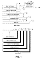
- FIG. 1 is a schematic block diagram illustrating a communications system with an integrated antenna and display in accordance with an aspect of the present invention.
- FIG. 2 is a schematic block diagram illustrating a communications system with an integrated antenna and display utilizing a pass-thru connection in accordance with an aspect of the present invention.
- FIG. 3 is a schematic block diagram illustrating a communications system with an integrated antenna and display utilizing a pass-over connection in accordance with an aspect of the present invention.
- FIG. 4 is a schematic block diagram illustrating a communications system with an integrated antenna and display utilizing a flexible circuit material pass-thru connection in accordance with an aspect of the present invention.
- FIG. 5 is a schematic block diagram illustrating a communications system with an integrated antenna and display utilizing a flexible circuit material pass-over connection in accordance with an aspect of the present invention.
- FIG. 6 is a schematic block diagram illustrating a communications and display system with and integrated antenna with a pass-thru connection in accordance with an aspect of the present invention.
- FIG. 7 is a schematic block diagram illustrating a communications and display system with and integrated antenna with a pass-over connection in accordance with an aspect of the present invention.
- FIG. 8 is a flow diagram illustrating a methodology providing integrated chip and display communications in accordance with the present invention.
- the present invention provides a system and methodology for creating a compact, reliable, low cost communications system through integration of a chip antenna, display lens and associated communications module.
- the chip antenna is protected from external elements, and is coupled to the display lens of the communications module. This prevents movement of the relative position of the antenna in relation to the communications module, facilitates consistent performance from one communications module to another, and decreases the probability of performance degradation due to sudden movements of or mechanical shock to the communications module.
- FIG. 1 illustrates a side view and a top view of respective antenna, circuit material, and display configurations in accordance with the present invention.
- the chip antenna 20 is operatively coupled to the circuit material 30 that is affixed to the conductive material 40 .
- the circuit material 30 provides an operative connection to the conductive material 40 wherein the conductive material 40 provides a ground connection and/or plane for the chip antenna 20 .
- a signal connection 49 operatively couples a received or transmitted RF signal (not shown) from the chip antenna 20 to the transmitter/receiver subsystem 44 .
- the transmitter/receiver subsystem 44 can be substantially any well-known communications interface for transmitting and/or receiving RF signals and providing subsequent RF signal processing. These interfaces may include cell-phones, pagers, Personal Digital Assistants (PDA), scanners (e.g., bar code) and hand-held or portable computers such as Palm Pilots.
- PDA Personal Digital Assistants
- scanners e.g., bar code
- Palm Pilots hand-held or portable computers
- the chip antenna 20 is mounted upon the circuit material 30 .
- the chip antenna 20 and circuit material 30 are then mounted upon the conductive material 40 to complete the signal transmitting/receiving portions of the communications system 10 a .
- the size relationship of chip antenna 20 and circuit material 30 to the conductive material 40 is not to scale in FIG. 1 . It is understood that the size relationship is dependent upon the desired frequency range of the chip antenna 20 .
- the conductive material 40 and associated lens material 46 may be substantially any size, but generally not smaller than is required to create a ground plane for the chip antenna 20 .
- the ground plane when coupled with chip antennas that operate in the four hundred (400) megahertz to twenty-four hundred (2400) megahertz range, the ground plane will be about ten (10) to thirty (30) times the size of the chip antenna.
- chip antenna 20 and circuit material 30 in reference to conductive material 40 and lens 46 is for clarity of illustration. It is to be appreciated that the chip antenna 20 may be placed at any suitable location on circuit material 30 , and that circuit material 30 may be placed at any suitable location on the conductive material 40 and lens 46 .
- the conductive material 40 that is utilized as the ground plane for chip antenna 20 can be substantially any conductive coating, treatment, film and/or screen mesh that is transparent/translucent to enable an unobstructed view of the display 48 through the lens material 46 .
- the lens material 46 is employed as a protective barrier for the display 48 .
- Many different materials may be employed in the construction of lenses, including but not limited to glass, Plexiglas and plastic, for example.
- the display 48 is employed to provide information that is related to the function of a communications module or device.
- the display 48 may be a liquid crystal display (LCD), cathode ray tube (CRT) or TFT panel, for example.
- a communications system 10 b illustrates an aspect of an exemplary chip antenna configuration and display in accordance with the present invention.
- the chip antenna 20 is coupled to circuit material 30 via solder connection 50 .
- the circuit material 30 is in the form of a substantially rigid printed circuit card, and is coupled to the conductive material 40 via a nonconductive adhesive 60 .
- the circuit material 30 is coupled to the transmitter/receiver subsystem 44 via mating connectors 72 and 74 through an opening 76 in the conductive material 40 and lens material 46 .
- the display 48 may also be provided with an opening wherein a coupling may be achieved from the circuit material 30 to the transmitter/receiver subsystem 44 .
- the opening 76 may be placed in any location on the conductive material 40 and lens material 46 that will facilitate the coupling of circuit material 30 and the transmitter/receiver subsystem 44 .
- the transmitter/receiver subsystem 44 includes mating connections 82 and 84 respectively for coupling to connectors 72 and 74 , wherein mating connector 82 provides a ground connection and mating connecting 84 provides an RF signal connection from the chip antenna 20 to the transmitter/receiver subsystem 44 .
- the connectors 72 , 74 , 82 and 84 may be commercially available connectors, custom designed connectors and/or provided by coupling wires to both the circuit material 30 and the transmitter/receiver circuit 44 . It is noted that the circuit material 30 is etched and/or fabricated such that there is an electrical coupling between the chip antenna 20 and mating connectors 72 and 74 .
- a communications system 10 c illustrates an alternative chip antenna and display in accordance with the present invention.
- the communications system 10 c is similar to the communications system 10 b described above with the exception of the placement of circuit material 30 with respect to conductive material 40 and lens material 46 .
- the circuit material 30 is placed such that mating connectors 72 and 74 are outside of the outer edge of conductive material 40 , lens material 46 and display 48 .
- This enables coupling of circuit material 30 to the transmitter/receiver subsystem 44 without an opening in the conductive material 40 and lens material 45 .
- Applications which do not have stringent space requirements may employ this configuration, as the manufacturing requirements are less demanding mitigating the need for openings in conductive material 40 and lens material 45 .
- the display 48 in this configuration may be placed such that it extends to the outer edge of lens material 45 and conductive material 40 . This enables a larger available viewing area of the display 48 .
- a system 10 d and 10 e illustrates an alternative circuit material, coupling and configuration in accordance with the present invention.
- the chip antenna 20 is coupled to circuit material 30 via solder connection 50 , as described above.
- the circuit material 30 is in the form of a flexible circuit strip or material, and is coupled to the conductive material 40 via a non-conductive adhesive 60 .
- the circuit material 30 is operatively coupled to the transmitter/receiver subsystem 44 via flexible connections 90 and 92 that are provided as part of the flexible circuit material 30 .
- the circuit material 30 is etched or fabricated such that there is an electrical coupling between chip antenna 20 and connections 90 and 92 . Referring to FIG.
- the communications system 10 e is similar to communications system 10 d with the exception of the coupling of the circuit material 30 .
- the circuit material 30 is coupled on the outside of the conductive material 40 , lens material 46 , and display 48 as illustrated.
- a communications system 10 f illustrates an integrated display system and antenna configuration.
- a bezel 110 is depicted on top of chip antenna 20 and circuit material 30 , and is constructed of a material that generally does not interfere with the signals being received and broadcast by the chip antenna 20 .
- the bezel 110 is employed to conceal and protect chip antenna 20 and circuit material 30 .
- the circuit material 30 is a substantially rigid circuit board, employed in a configuration similar to that described for display system 10 b in FIG. 2 .
- the location of the chip antenna 20 utilizes the bezel 110 as a protective and aesthetically pleasing barrier while providing for optimal signal strength by placing the chip antenna 20 outside of a communications module housing (not shown) interfacing to the bezel 110 .
- the display 48 is installed in the system such that it does not interfere mechanically with the mating connectors 72 , 74 , 82 and 84 or the opening 76 in conductive material 40 and lens material 45 . It is to be appreciated that other display configurations are possible. For example, a flexible circuit as depicted in the communications system 10 d in FIG. 4 may also be employed with the display illustrated in FIG. 6 .
- a communications system 10 g illustrates an alternative integrated display system and antenna configuration. This configuration is similar to that described above for the display system 10 g with the exception of the placement of chip antenna 20 and circuit material 30 with respect to conductive material 40 and lens material 45 .
- the circuit material 30 is mounted such that the flexible circuit connection to the transmitter/receiver subsystem 44 is outside of the outer edge of conductive material 40 , lens material 45 and display 48 . This enables coupling of the circuit material 30 to transmitter/receiver subsystem 44 without an opening in the conductive material 40 and the lens material 45 .
- a connection as depicted in the communications system 10 c in FIG. 3 may also be employed with the display illustrated in FIG. 7 .
- FIG. 8 illustrates a methodology for providing an integrated chip antenna and display in accordance with an aspect of the present invention. While, for purposes of simplicity of explanation, the methodology is shown and described as a series of acts, it is to be understood and appreciated that the present invention is not limited by the order of acts, as some acts may, in accordance with the present invention, occur in different orders and/or concurrently with other acts from that shown and described herein. For example, those skilled in the art will understand and appreciate that a methodology could alternatively be represented as a series of interrelated states or events, such as in a state diagram. Moreover, not all illustrated acts may be required to implement a methodology in accordance with the present invention.
- a chip antenna is operatively coupled to a circuit material.
- a conductive material is applied to a lens material of a display. As described above, the conductive material should be substantially transparent so as not to obstruct a display.
- the circuit material is coupled to the lens material that was coated with the conductive material at 210 . As described above, the conductive material provides a suitable ground plane for the chip antenna. This step may be achieved through various techniques, including but not limited to fasteners and adhesives.
- the lens material is coupled to a display, wherein information is presented to a user relating to a communications module or subsystem.
- the circuit material is coupled to a communications module such as a transmitter/receiver subsystem described above.
Landscapes
- Engineering & Computer Science (AREA)
- Computer Hardware Design (AREA)
- General Engineering & Computer Science (AREA)
- Support Of Aerials (AREA)
- Transceivers (AREA)
Abstract
Description
Claims (26)
Priority Applications (1)
| Application Number | Priority Date | Filing Date | Title |
|---|---|---|---|
| US10/085,537 US6774847B1 (en) | 2001-03-01 | 2002-02-28 | System and method providing integrated chip antenna with display for communications devices |
Applications Claiming Priority (2)
| Application Number | Priority Date | Filing Date | Title |
|---|---|---|---|
| US27268401P | 2001-03-01 | 2001-03-01 | |
| US10/085,537 US6774847B1 (en) | 2001-03-01 | 2002-02-28 | System and method providing integrated chip antenna with display for communications devices |
Publications (1)
| Publication Number | Publication Date |
|---|---|
| US6774847B1 true US6774847B1 (en) | 2004-08-10 |
Family
ID=32829231
Family Applications (1)
| Application Number | Title | Priority Date | Filing Date |
|---|---|---|---|
| US10/085,537 Expired - Fee Related US6774847B1 (en) | 2001-03-01 | 2002-02-28 | System and method providing integrated chip antenna with display for communications devices |
Country Status (1)
| Country | Link |
|---|---|
| US (1) | US6774847B1 (en) |
Cited By (6)
| Publication number | Priority date | Publication date | Assignee | Title |
|---|---|---|---|---|
| US6982879B1 (en) * | 2003-07-19 | 2006-01-03 | Intel Corporation | Apparatus to provide connection between a microelectronic device and an antenna |
| US20100261445A1 (en) * | 2007-12-06 | 2010-10-14 | Fredrik Harrysson | Display arrangement |
| US20120287018A1 (en) * | 2011-05-11 | 2012-11-15 | Harris Corporation, Corporation Of The State Of Delaware | Electronic device including a patch antenna and photovoltaic layer and related methods |
| WO2012154391A2 (en) | 2011-05-11 | 2012-11-15 | Harris Corporation | Electronic device including a patch antenna and visual display layer and related methods |
| WO2012154389A2 (en) | 2011-05-10 | 2012-11-15 | Harris Corporation | Electronic device including electrically conductive mesh layer patch antenna and related methods |
| CN112333307A (en) * | 2020-10-29 | 2021-02-05 | 维沃移动通信有限公司 | Display module and electronic device |
Citations (4)
| Publication number | Priority date | Publication date | Assignee | Title |
|---|---|---|---|---|
| US5909198A (en) * | 1996-12-25 | 1999-06-01 | Murata Manufacturing Co., Ltd. | Chip antenna |
| US5986614A (en) * | 1997-02-24 | 1999-11-16 | Murata Manufacturing Co., Ltd. | Antenna device |
| US6031731A (en) * | 1997-05-14 | 2000-02-29 | Murata Manufacturing Co., Ltd. | Mobile communication apparatus having a selecting plate mounted on circuit board |
| US6442399B1 (en) * | 1995-08-07 | 2002-08-27 | Murata Manufacturing Co., Ltd. | Mobile communication apparatus |
-
2002
- 2002-02-28 US US10/085,537 patent/US6774847B1/en not_active Expired - Fee Related
Patent Citations (4)
| Publication number | Priority date | Publication date | Assignee | Title |
|---|---|---|---|---|
| US6442399B1 (en) * | 1995-08-07 | 2002-08-27 | Murata Manufacturing Co., Ltd. | Mobile communication apparatus |
| US5909198A (en) * | 1996-12-25 | 1999-06-01 | Murata Manufacturing Co., Ltd. | Chip antenna |
| US5986614A (en) * | 1997-02-24 | 1999-11-16 | Murata Manufacturing Co., Ltd. | Antenna device |
| US6031731A (en) * | 1997-05-14 | 2000-02-29 | Murata Manufacturing Co., Ltd. | Mobile communication apparatus having a selecting plate mounted on circuit board |
Cited By (11)
| Publication number | Priority date | Publication date | Assignee | Title |
|---|---|---|---|---|
| US6982879B1 (en) * | 2003-07-19 | 2006-01-03 | Intel Corporation | Apparatus to provide connection between a microelectronic device and an antenna |
| US20100261445A1 (en) * | 2007-12-06 | 2010-10-14 | Fredrik Harrysson | Display arrangement |
| US8543167B2 (en) * | 2007-12-06 | 2013-09-24 | Telefonaktiebolaget Lm Ericsson (Publ) | Display arrangement |
| WO2012154389A2 (en) | 2011-05-10 | 2012-11-15 | Harris Corporation | Electronic device including electrically conductive mesh layer patch antenna and related methods |
| US8786516B2 (en) | 2011-05-10 | 2014-07-22 | Harris Corporation | Electronic device including electrically conductive mesh layer patch antenna and related methods |
| US20120287018A1 (en) * | 2011-05-11 | 2012-11-15 | Harris Corporation, Corporation Of The State Of Delaware | Electronic device including a patch antenna and photovoltaic layer and related methods |
| WO2012154391A2 (en) | 2011-05-11 | 2012-11-15 | Harris Corporation | Electronic device including a patch antenna and visual display layer and related methods |
| WO2012154390A2 (en) | 2011-05-11 | 2012-11-15 | Harris Corporation | Electronic device including a patch antenna and photovoltaic layer and related methods |
| US8665161B2 (en) | 2011-05-11 | 2014-03-04 | Harris Corporation | Electronic device including a patch antenna and visual display layer and related methods |
| US8872711B2 (en) * | 2011-05-11 | 2014-10-28 | Harris Corporation | Electronic device including a patch antenna and photovoltaic layer and related methods |
| CN112333307A (en) * | 2020-10-29 | 2021-02-05 | 维沃移动通信有限公司 | Display module and electronic device |
Similar Documents
| Publication | Publication Date | Title |
|---|---|---|
| CN207218688U (en) | Electronic equipment | |
| EP3602236B1 (en) | Shielding a bending portion of a flexible display | |
| CN207074710U (en) | Electronic equipment | |
| CN107210516B (en) | Antenna device and electronic device comprising same | |
| CN205752546U (en) | Equipment with the radiating element from conduction wearable device carrier arrangement isolation | |
| US20210104814A1 (en) | Display Device with Integrated Antenna | |
| CN108039571A (en) | Center component, antenna module and electronic equipment | |
| US6831561B2 (en) | Communications system and method with A/D converter | |
| EP3593339B1 (en) | Electronic price label and electronic price label system | |
| US20070176843A1 (en) | RF communication system with embedded antenna | |
| KR20180137212A (en) | An electronic device comprising antenna | |
| US11005154B2 (en) | Antennas in frames for display panels | |
| CN108321495A (en) | Antenna module, antenna assembly and electronic equipment | |
| CN105938933A (en) | Portable electronic device with antenna | |
| CN1524317A (en) | Wristwatch with antenna | |
| CN110554526A (en) | Liquid crystal display device with built-in antenna coil | |
| US6774847B1 (en) | System and method providing integrated chip antenna with display for communications devices | |
| CN110431830B (en) | Electronic device including antenna | |
| US11671127B2 (en) | Antenna module, terminal, control method and device and storage medium | |
| US6768467B2 (en) | Method of RF grounding glass mounted antennas to automotive metal frames | |
| CN113745805A (en) | Antenna receiving device and electronic timepiece | |
| US6922575B1 (en) | Communications system and method utilizing integrated chip antenna | |
| US11990968B2 (en) | Radio frequency module and electronic device | |
| KR101041356B1 (en) | Multi-band antenna and telematics apparatus having the same | |
| EP1887457B1 (en) | Display system of a vehicle electronic system |
Legal Events
| Date | Code | Title | Description |
|---|---|---|---|
| AS | Assignment |
Owner name: SYMBOL TECHNOLOGIES, INC., NEW YORK Free format text: ASSIGNMENT OF ASSIGNORS INTEREST;ASSIGNOR:TELXON CORPORATION;REEL/FRAME:012795/0070 Effective date: 20020327 |
|
| AS | Assignment |
Owner name: TELXON CORPORATION, NEW YORK Free format text: ASSIGNMENT OF ASSIGNORS INTEREST;ASSIGNORS:EPSTEIN, NORMAN;VU, ROBERT;REEL/FRAME:012861/0952;SIGNING DATES FROM 20020108 TO 20020415 |
|
| AS | Assignment |
Owner name: JPMORGAN CHASE BANK, N.A., NEW YORK Free format text: SECURITY INTEREST;ASSIGNOR:SYMBOL TECHNOLOGIES, INC.;REEL/FRAME:016116/0203 Effective date: 20041229 |
|
| FPAY | Fee payment |
Year of fee payment: 4 |
|
| AS | Assignment |
Owner name: SYMBOL TECHNOLOGIES, INC., NEW YORK Free format text: RELEASE BY SECURED PARTY;ASSIGNOR:JPMORGANCHASE BANK, N.A.;REEL/FRAME:025441/0228 Effective date: 20060901 |
|
| REMI | Maintenance fee reminder mailed | ||
| LAPS | Lapse for failure to pay maintenance fees | ||
| STCH | Information on status: patent discontinuation |
Free format text: PATENT EXPIRED DUE TO NONPAYMENT OF MAINTENANCE FEES UNDER 37 CFR 1.362 |
|
| FP | Expired due to failure to pay maintenance fee |
Effective date: 20120810 |