EP0874920B1 - Procede et dispositif pour le traitement electrochimique de produits au moyen d'un liquide de traitement - Google Patents
Procede et dispositif pour le traitement electrochimique de produits au moyen d'un liquide de traitement Download PDFInfo
- Publication number
- EP0874920B1 EP0874920B1 EP97914313A EP97914313A EP0874920B1 EP 0874920 B1 EP0874920 B1 EP 0874920B1 EP 97914313 A EP97914313 A EP 97914313A EP 97914313 A EP97914313 A EP 97914313A EP 0874920 B1 EP0874920 B1 EP 0874920B1
- Authority
- EP
- European Patent Office
- Prior art keywords
- electrodes
- brush
- treated
- brush electrodes
- transport path
- Prior art date
- Legal status (The legal status is an assumption and is not a legal conclusion. Google has not performed a legal analysis and makes no representation as to the accuracy of the status listed.)
- Expired - Lifetime
Links
Images


Classifications
-
- H—ELECTRICITY
- H05—ELECTRIC TECHNIQUES NOT OTHERWISE PROVIDED FOR
- H05K—PRINTED CIRCUITS; CASINGS OR CONSTRUCTIONAL DETAILS OF ELECTRIC APPARATUS; MANUFACTURE OF ASSEMBLAGES OF ELECTRICAL COMPONENTS
- H05K3/00—Apparatus or processes for manufacturing printed circuits
- H05K3/02—Apparatus or processes for manufacturing printed circuits in which the conductive material is applied to the surface of the insulating support and is thereafter removed from such areas of the surface which are not intended for current conducting or shielding
- H05K3/06—Apparatus or processes for manufacturing printed circuits in which the conductive material is applied to the surface of the insulating support and is thereafter removed from such areas of the surface which are not intended for current conducting or shielding the conductive material being removed chemically or electrolytically, e.g. by photo-etch process
- H05K3/07—Apparatus or processes for manufacturing printed circuits in which the conductive material is applied to the surface of the insulating support and is thereafter removed from such areas of the surface which are not intended for current conducting or shielding the conductive material being removed chemically or electrolytically, e.g. by photo-etch process being removed electrolytically
-
- C—CHEMISTRY; METALLURGY
- C25—ELECTROLYTIC OR ELECTROPHORETIC PROCESSES; APPARATUS THEREFOR
- C25D—PROCESSES FOR THE ELECTROLYTIC OR ELECTROPHORETIC PRODUCTION OF COATINGS; ELECTROFORMING; APPARATUS THEREFOR
- C25D17/00—Constructional parts, or assemblies thereof, of cells for electrolytic coating
- C25D17/005—Contacting devices
-
- C—CHEMISTRY; METALLURGY
- C25—ELECTROLYTIC OR ELECTROPHORETIC PROCESSES; APPARATUS THEREFOR
- C25D—PROCESSES FOR THE ELECTROLYTIC OR ELECTROPHORETIC PRODUCTION OF COATINGS; ELECTROFORMING; APPARATUS THEREFOR
- C25D17/00—Constructional parts, or assemblies thereof, of cells for electrolytic coating
- C25D17/008—Current shielding devices
-
- C—CHEMISTRY; METALLURGY
- C25—ELECTROLYTIC OR ELECTROPHORETIC PROCESSES; APPARATUS THEREFOR
- C25D—PROCESSES FOR THE ELECTROLYTIC OR ELECTROPHORETIC PRODUCTION OF COATINGS; ELECTROFORMING; APPARATUS THEREFOR
- C25D5/00—Electroplating characterised by the process; Pretreatment or after-treatment of workpieces
- C25D5/02—Electroplating of selected surface areas
-
- C—CHEMISTRY; METALLURGY
- C25—ELECTROLYTIC OR ELECTROPHORETIC PROCESSES; APPARATUS THEREFOR
- C25F—PROCESSES FOR THE ELECTROLYTIC REMOVAL OF MATERIALS FROM OBJECTS; APPARATUS THEREFOR
- C25F7/00—Constructional parts, or assemblies thereof, of cells for electrolytic removal of material from objects; Servicing or operating
-
- H—ELECTRICITY
- H05—ELECTRIC TECHNIQUES NOT OTHERWISE PROVIDED FOR
- H05K—PRINTED CIRCUITS; CASINGS OR CONSTRUCTIONAL DETAILS OF ELECTRIC APPARATUS; MANUFACTURE OF ASSEMBLAGES OF ELECTRICAL COMPONENTS
- H05K3/00—Apparatus or processes for manufacturing printed circuits
- H05K3/22—Secondary treatment of printed circuits
- H05K3/24—Reinforcing the conductive pattern
- H05K3/241—Reinforcing the conductive pattern characterised by the electroplating method; means therefor, e.g. baths or apparatus
Definitions
- the invention relates to a method for the electrochemical treatment of Material to be treated with a treatment liquid and a device for Execution of the procedure.
- conductive surfaces must be on their surfaces Structures, the traces, are formed. These face each other isolated islands to be treated selectively.
- the structures on material to be treated for example on printed circuit boards, each must have an electrically conductive connection for treatment to the bath power source, since an electrochemical treatment of The material to be treated generally presupposes that those to be treated Surfaces are electrically conductive.
- electrochemical Process is therefore used to treat structures on printed circuit boards a fully metallized and possibly plated through and electrolytically reinforced with copper circuit board.
- the Printed circuit boards prepared in this way are used to print the structures or photographically, for example with a negative structure image, upset. Then the not covered electrically conductive surfaces selectively treated electrochemically. In the As a rule, several process steps are required for this.
- the electrically conductive Layer between the structures can be completely removed by etching.
- the etching process is preferably used in chemical baths spraying and spraying technology.
- the disadvantage of this method is that the material to be treated is twice in a wet chemical treatment line has to be run in: First the circuit boards are plated through. After that, the plates printed with the structure image outside the wet area and then they are used again to treat the structures in a wet chemical Treatment line retracted. Appropriate rinsing and drying processes are necessary. It is also disadvantageous that the conductive base layer between the structures only after completion of the ladder lines can be removed. To do this, the surfaces of the conductor tracks must be included an additional protection to be provided in order not in the etching process to be damaged.
- the published patent application DE 43 37 988 A1 describes a manufacturing process of multilayer inner layers. It is suggested that Oxidized copper surfaces electrochemically in a horizontal continuous system to reduce. A salt solution, for example, is said to be the electrolyte be used. Over one or two pairs of rollers per multilayer layer the oxidized surfaces become electrical with cathodic polarity contacted by the structures with the bath power source over the rollers be electrically connected. The anodes are arranged so that the Treated goods can be transported between them. By Electrolysis occurs on the cathodically polarized surfaces of the hydrogen in an atomic form that reduces the copper oxide. The effort for this is small compared to chemical reduction.
- a disadvantage of this method is that the contact time on the rollers is very small during the run.
- a conductor track or an isolated one Soldering eye with a dimension of one millimeter in the direction of transport Printed circuit boards are only at a transport speed of 1 m / min contacted during the very short period of about 0.06 seconds.
- this short period of time is much too much for electrochemical treatment low.
- Other conductor tracks on the conductor foil, which are parallel to the transport direction are essential according to their length longer contact time. The result is that the effective treatment time of the orientation of the structures on the material to be treated is dependent.
- Another disadvantage is that the contact rollers are very precise need to cover all mutually insulated copper surfaces along the surface line to contact and treat with it.
- rollers With cathodic switching the rollers also tend to accumulate contaminants, some of which adhere very firmly. This makes it even Contacting the treatment goods further difficult. It is the electrochemical process around a galvanizing process the rollers are also very heavily metallized, so that a continuous Continuous operation with this procedure is not possible.
- the roller contact is unsuitable even if the Structures should only be partially treated electrochemically.
- the areas not to be treated for example with solder mask covered.
- the areas to be treated which are then lower can be from the contact rollers cannot be reached.
- US-A 51 14 558 Another method and a device suitable therefor are known from US-A 51 14 558 known.
- this device contains Contacting the conductor tracks a variety of arranged in two levels Brush fibers that are perpendicular to a transport direction of the printed circuit boards on both sides of the circuit boards. These brushes are with one Power source connected and when etching the structures from all over Lamination anodically poled.
- a counter electrode is from the PCB level seen from beyond the brush assembly, which is also provided connected to the power source and cathodic in the arrangement shown is poled.
- this device is not suitable, with sufficient high currents an electrochemical treatment of the metallic surfaces to perform on the circuit boards because the counter electrode through the Brushing is completely shielded. It can even be assumed that with this arrangement on the circuit boards no electrical current at all can be generated. Rather, all electrochemical processes play out within a gap between the counter electrodes and the brushes.
- C-581 is a device disclosed in the circuit boards by a with a metallization bath filled metallization container and with a rotating Brush roller trained electrode to be brought in contact Insulated electrical conductors arranged on the printed circuit boards are electrolytically supplied metallize.
- the device contains a counter electrode designed as a plate, the one next to the rotating brush roller and the circuit board is arranged.
- the present invention is therefore based on the problem.
- the procedure and the device may be suitable for the circuit boards in continuous systems, in which the circuit boards are held in a horizontal or vertical position, treat and treat structures made up of very small isolated areas exist, and / or only a partial treatment of to enable electrically conductive structures.
- An essential aspect The invention also relates to the problem that contacting elements in the electrolytic metal deposition, the metal also on the contacting elements precipitates so that appropriate measures are taken to solve this problem.
- material to be treated can by means of suitable transport devices on a transport track are conveyed through the device.
- suitable ones are also available Devices for guiding or taking up the treatment liquid provided that are arranged so that the goods when transported by the Device at least temporarily in contact with the treatment liquid is brought, for example by immersion or flooding.
- It are all electrically conductive areas that are electrically insulated from one another on the material to be treated, for example the printed circuit boards, with stationary, powered by a power source through electrical connections Brush electrodes brought into contact at least one after the other, so that on the areas have an electrical potential, while the areas with the treatment liquid are in contact.
- each electrically insulating release agent arranged to a direct Current flow between the counter electrodes and the brush electrodes too prevent.
- a preferred application of the method according to the invention or preferred embodiment of the device consists in printed circuit boards to be treated continuously in a continuous system.
- the plates by means of suitable transport devices, for example Rollers or wheels, in the horizontal transport direction through the system conveyed and get into a bath of treatment liquid, for example or are swallowed up by suitable facilities or sprayed.
- the circuit boards can be stored horizontally or vertically be.
- the brush electrodes and counter electrodes for electrochemical Treatment is preferably on both sides of the conveyor belt, i.e. for example above and below the transport level. Therefore the plates are conveyed between the electrodes.
- the electrodes can of course only on one side of the PCB be arranged.
- the brush electrodes and the counter electrodes near the Transport path seen in the direction of transport or another direction preferably arranged alternately so that the counter electrodes between those lying side by side on one side of the item to be treated arranged brush electrodes are arranged.
- the brushes consist of fine-wire, electrically conductive fibers. she are preferably within the treatment liquid under the Bath mirrors are arranged and are preferably in the form of parallel to each other aligned rows formed. These rows can be at an angle greater than zero to the direction of transport of the material to be treated, preferably perpendicular to the direction of transport, and parallel to that, preferably in shape a transport level trained transport track can be arranged.
- Brushes made of resistant materials such as titanium, niobium, tantalum, Precious metals or stainless steel.
- the fibers of the brush for example with a Fiber diameters of 0.01 mm are very elastic. You adapt to that treating surface very well. This also enables partial Treatment of structures that lie deeper than adjacent insulating layers these areas (for example a solder mask). The tufts of fibers reach even the smallest areas between these insulations. The fine-stranded fibers cause on the surfaces to be treated no damage due to its elasticity. In conjunction with a A large number of fibers per brush results with an appropriate arrangement of many brushes at right angles to the transport direction of the material to be treated a long contact time of the individual structures.
- electrochemical processes where no metal is deposited, the contact time can be almost 100 Reach percent because the counter electrodes are close to the brushes can be arranged. That means that every isolated structure during the passage through the electrochemical bath despite the the spacing of the brush electrodes from one another due to the counter electrodes is always in electrical contact with the bath power source.
- electrochemical processes are, for example, electrolytic cleaning, Oxidize, reduce and etch (deburr).
- the brushes and the material to be treated are anodized or poled cathodically.
- the method according to the invention is also particularly suitable for such electrochemical processes in which metals are on the material to be treated be deposited. Examples of this are the selective separation of Copper, gold, nickel, tin as well as tin / lead, copper / tin and copper / zinc alloys on structured printed circuit boards.
- the method is also suitable and the device for the fully additive manufacturing of printed circuit boards by electrochemical metal deposition, in particular by copper deposition.
- electrolytic metal deposition the brushes are electrodes connected cathodically. This means that the electrical is not isolated surface areas of the brushes, as well as the material to be treated themselves, be galvanized. Therefore, they need to be demetallized from time to time become. To largely avoid fiber electroplating each individual fiber must be insulated like an insulated fine wire.
- the brush electrodes In processes where metal is on the electrically conductive areas is separated, the brush electrodes must be regularly removed from the metal be freed again.
- the brushes are made removed from the device and in a separate device by chemical or electrochemical etching removes any attached metal.
- the brush electrodes must be designed so that they are light are interchangeable.
- insoluble anodes are used.
- At least two in the form of preferably arranged in parallel Rows of brush electrodes are across or at any angle to Transport direction of the printed circuit boards arranged. Preferably extend these rows extend across the entire width of the transport path or of the width to be used or at least about the width that is covered by the electrically conductive areas.
- individual ones of the brush electrodes or rows of brush electrodes are used by means of suitable devices from the circuit board surfaces lifted off by a distance between the electrodes and the Transport path is made so that they do not to the circuit boards Have more contact.
- the brush electrodes are by means of further suitable devices at least temporarily reversed. Thereby some of the brush electrodes act as, for example, during metallization cathodic contacting for the printed circuit boards and the other part than insoluble anodes. Furthermore, the polarity-reversed brush electrodes are in this condition is also anodically polarized compared to the other brushes.
- the Lifted brushes are electrochemically demetallized, the others Brushes lead the cathode potential to the surfaces of the treatment Structures. These structures and the latter brushes will be metallized. After a preselectable time, the switching states of the Brushes changed. The metallized brushes are switched as anodes, and the demetallized brushes are switched as cathodes. Demetalization and metallization are carried out accordingly. The described interplay the brushes can alternate with many rows of brushes in the System take place so that a long effective cathodic contact time is achieved.
- the amount of metal deposited on the PCB surfaces must be in the bathroom are continuously supplemented. This is done using known means and methods, for example by adding metal salts.
- the brush electrodes can also by means of a demetallization substrate, preferably in the form of a Plate which, like the material to be treated, is transported through the conveyor belt Plant is transported to be freed of accumulated metal.
- a demetallization substrate preferably in the form of a Plate which, like the material to be treated, is transported through the conveyor belt Plant is transported to be freed of accumulated metal.
- Another device is used to control this process, with which the transport of the substrate in the device can be followed.
- the plate itself is preferably connected cathodically. On it will the metal is removed electrolytically from the brushes.
- the brush electrodes do not have to be from the transport level be lifted off if the demetallizing substrate with a diaphragm is coated, an electrical short circuit of the bath power source prevented.
- the brush electrodes which are preferably in the form of rows for removing accumulated metal from the material to be treated, in particular the printed circuit boards, electrically reversed, which the demetallization substrate transports past becomes.
- the demetallization substrate can preferably be in a continuous path in the device are transported. This serves on part of the track Substrate for the demetallization of the brush electrodes in the specified Wise. On another part of the train, preferably on the way back the demetallization substrate becomes the starting point of the first part of the path itself either chemically or electrochemically from that freed deposited metal by placing it in a suitable demetallization bath, optionally with further electrodes for electrochemical Demetallization, immersed.
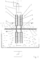
- FIG. 1 there are structures 2 on both sides of the printed circuit board 1 are to be treated electrochemically, here galvanized.
- the structures are electrically conductive. For example, they can be created by etching and have no electrical connection with each other. So is a Contact the structures in a single location on the circuit board like it is common from the known methods for the production of printed circuit boards, not possible.
- the device serves the metallic fibers 3 of the brushes 4.
- the fibers 3 lie slightly on the surfaces of the structures 2 to be treated. she thus together with the lines 6 provide the electrical connection of the surfaces over the brushes 4 to the bath current source 7.
- the other Pole of the bath current source 7 is connected to the counter electrode 8. This The electrode is electrically insulated between the brushes 4.
- the active one Electrode surface 9 is in the vicinity of the electrically contacted Structures 2.
- the bath current source 7 is shown poled so that the device for example for electrochemical demetallization the PCB is suitable.
- the counterelectrode 8 is closed from time to time demetallize. This can be done by cyclical electrode exchange, by removing the electrodes from the device and placing them in a separate Device can be demetallized. With electrochemical reduction without dissolved metal in the treatment solution, the exchange of the Brush because nothing is deposited on them.
- the brushes 10, 11, 12, 13 are arranged movably. Each two brushes are carried by a rocker 14.
- the preferred Current-controlled bath current source 7 is here for the brushes 10 and 12 poled as it is necessary for electroplating.
- the brushes 10 and 12 have via the switch 15 therefore cathodic potential. They are about Structures 2 electrically contacted on the circuit board.
- the through the seesaw 14 lifted brushes 11 and 13 are anodic via the switch 15 poled. They act as anodes. At the same time, they are demetallized if they were previously galvanized.
- a partition 16 between each two brushes acts electrically insulating, so that a direct current flow between the differently polarized brush electrodes is largely prevented.
- the brushes 11 and 13 After the demetallization of the brushes 11 and 13 are completed brought to the circuit board surface by means of the rockers 14 while at the same time the brushes 10 and 12 are lifted off the surface.
- the polarity of the brushes changes as shown.
- the brushes can preferably be arranged closer together as shown in Figure 2.
- the lifting and lowering brushing can also be done by other mechanical means. It is not limited to seesaws. Switching the polarities of the Brushing is also possible with electronic switches. That of continuous systems known transport rollers or wheels 17 are only shown in FIG. 2 shown.
- Such transport organs can also in the devices of Figures 1 and 3 are used to the circuit boards along the indicated by the arrow shown transport direction through the Transport device.
- rollers can also be used for this to the treatment liquid located above the transport level to prevent it from entering and leaving the device to resign.
- FIG. 1 A further embodiment of the invention is shown in FIG.
- the brush electrodes 21 are movable. You can use a drive, not shown, to move individually from the treating circuit board 23 or of a metallic Demetallization plate 24 are lifted off. Over the continuous Plate 24, the brushes 21 are lifted off. Resting on the circuit board 23 Fibers of the brushes provide the electrical connection between those to be treated Structures via lines 25 to the changeover switch 26. About him is the negative pole of the bath current source 27 with the galvanizing Brushes connected.
- the electroplating current is automatically adjusted accordingly the selected current density depending on the number of each cathodically switched brushes set. For this, the material to be treated, the circuit board 23 or the circuit board from the control system of the continuous system. Switching the on and off Brushing is done individually in the correct order.
- the brushes can in an analogous manner, as it is in the patent DE 39 39 681 C2 for switching anodes in continuous systems is described become. Regarding the type and implementation of this control referred to this publication.
- the anodes 20 are preferably insoluble.
- the solution in the electrolyte Metal is not only on the structures of the circuit board 23, but also deposited on the fibers or fiber tips of the brushes. she must be demetallized from time to time.
- Figure 3 is the transition from metallization to demetallization.
- the brushes 21 are raised and at the same time on the switch 26 an anodic potential.
- The serves for demetallization individually adjustable second current source 28.
- the negative pole of the current source 28 is with the demetallization plate 24 is electrically connected.
- To contact the like the printed circuit boards to be transported through the system 24 serve sliding contacts 29 or brackets, as of horizontal electroplating systems are known.
- the metal on the demetallization plates 24 separates the fibers of the brushes.
- the brushes work practically up to for complete metal detachment as soluble anodes, for metal dissolution a bath voltage about 0.8 volts lower than insoluble anodes require. It follows that the insoluble anodes 20 because of the for they do not start at low potential and no electroplating current to lead. When the metal has completely detached from the fibers, place it these are also insoluble anodes. The anode current then drops Values from about zero. This circumstance can initiate the reversal the brushes are used. If soluble anodes 20 are used, it is expedient to use an electrically not shown Disconnect switch from the positive potential of the rail 30 when in this area is being demetallized.
- the demetallization plate 24 and the sliding contacts 29 or clamps can be returned chemically or electrochemically to the system feed be demetallized.
- the plates can also be another Metal recovery can be fed.
- the Brushes 21 can be dispensed with when demetallizing.
- the demetallization plate 24 Covered on all sides with a thin, electrically non-conductive diaphragm. The only exceptions to this are the side areas for contacting the plate. These areas are not covered by the brushes.
- the diaphragm can be a chemically resistant cloth. Suitable for this is for example a polypropylene fabric.
- the anodically switched Brushes are demetallized via the diaphragm. The demetallization process is because of the particularly small anode / cathode spacing highly effective. This allows the length of the current demetallation section to keep it short compared to the metallization path. With the diaphragm-covered demetallization plates are also through the diaphragm in a separate part of the transport path demetallized. This demetallization can preferably also be electrochemical be performed.
- the device can also be used to treat the printed circuit boards on both sides Figure 3 be constructed in mirror image.
Landscapes
- Chemical & Material Sciences (AREA)
- Engineering & Computer Science (AREA)
- Materials Engineering (AREA)
- Chemical Kinetics & Catalysis (AREA)
- Electrochemistry (AREA)
- Metallurgy (AREA)
- Organic Chemistry (AREA)
- Microelectronics & Electronic Packaging (AREA)
- Manufacturing & Machinery (AREA)
- Electroplating Methods And Accessories (AREA)
- Manufacturing Of Printed Wiring (AREA)
- Water Treatment By Electricity Or Magnetism (AREA)
- Electrotherapy Devices (AREA)
Claims (18)
- Procédé de traitement électrochimique de zones électroconductrices isolées électriquement les unes des autres, sur un élément à traiter, au moyen d'un liquide de traitement, dans lequelcaractérisé en ce quea. l'élément à traiter est acheminé à travers le dispositif sur une voie de transport au moyen d'installations de transport, et est en l'occurrence mis en contact avec le liquide de traitement au moins temporairement,b. toutes les zones électroconductrices sur l'élément à traiter sont mises en contact au moins l'une après l'autre avec des électrodes-balais fixes, alimentées par une source de courant, de telle sorte qu'il existe un potentiel électrique au niveau des zones électroconductrices, tandis que les zones se trouvent également en contact avec le liquide de traitement,c. dans lequel sont en outre prévues, à proximité de la voie de transport, des contre-électrodes également alimentées par la source de courant avec une polarité inverse, ces contre-électrodes étant disposées de telle sorte qu'un courant électrique puisse circuler entre les zones électroconductrices et les contre-électrodes,d. entre les électrodes-balais et les contre-électrodes sont respectivement disposés des moyens séparateurs assurant une isolation électrique, afin d'empêcher un passage de courant entre les contre-électrodes et les électrodes-balais.
- Procédé selon la revendication 1, caractérisé en ce que les électrodes-balais sont de nouveau débarrassées du métal déposé lors du traitement.
- Procédé selon la revendication 2, caractérisé en ce que, pour éliminer le métal déposé, des électrodes-balais individuelles sont retirées de la voie de transport et subissent alors une inversion de leur polarité électrique.
- Procédé selon la revendication 3. caractérisé en ce qu'un substrat de démétallisation est transporté sur la voie de transport à travers le dispositif et une distance est établie entre la voie de transport et les différentes électrodes-balais, ce qui entraíne une inversion de la polarité des électrodes-balais devant lesquelles passe le substrat de démétallisation.
- Procédé selon la revendication 2, caractérisé en ce qu'un substrat de démétallisation recouvert d'un diaphragme est transporté sur la voie de transport à travers le dispositif, ce qui entraíne une inversion de la polarité électrique des différents électrodes-balais devant lesquelles passe le substrat de démétallisation, afin d'éliminer le métal déposé.
- Procédé selon l'une des revendications 4 et 5, caractérisé en ce que le substrat de démétallisation est polarisé de manière cathodique par rapport aux électrodes-balais dont la polarité a été inversée.
- Procédé selon l'une quelconque des revendications 4 à 6, caractérisé en ce que le substrat de démétallisation est transporté sur une voie sans fin dans le dispositif, le substrat étant acheminé sur un tronçon de voie afin de démétalliser les électrodes-balais et étant de nouveau démétallisé sur un autre tronçon.
- Procédé selon l'une quelconque des revendications 3 à 7, caractérisé en ce qu'une densité de courant élevée est établie au niveau des électrodes-balais, lorsque la polarité de ces dernières est inversée.
- Procédé selon la revendication 2, caractérisé en ce que les électrodes-balais sont de nouveau débarrassées du métal déposé en éloignant les électrodes-balais de dispositif ou en corrodant par voie chimique oux électrochimique le métal des électrodes-balais.
- Dispositif de traitement électrochimique de zones électroconductrices isolées électriquement les unes des autres. sur un élément à traiter, au moyen d'un liquide de traitement. présentantcaractérisé en ce quea. des installations de transport de l'élément sur une voie de transport à travers le dispositif,b. d'autres installations destinées à l'acheminement ou à la réception du liquide de traitement, ces installations étant disposées de telle sorte que l'élément vienne au contact du liquide de traitement au moins temporairementc. en outre des électrodes-balais fixes disposées de telle sorte que, durant le transport de l'élément sur la voie de transport, ces électrodes soient mises en contact au moins l'une après l'autre avec toutes les zones électroconductrices, tandis que les zones sont également en contact avec le liquide de traitement,d. des contre-électrodes, qui sont disposées à proximité de la voie de transport de telle sorte qu'un courant électrique puisse circuler entre les zones électroconductrices et les contre-électrodes,e. une source de courant et des connexions entre la source de courant et les électrodes afin d'alimenter les électrodes en courant,f. entre les électrodes-balais (4, 10, 12, 21) et les contre-électrodes (8, 11, 13) sont disposés respectivement des moyens séparateurs isolants électriquement, afin d'empêcher un passage de courant direct entre les contre-électrodes et les électrodes-balais.
- Dispositif selon la revendication 10, caractérisé en ce que les électrodes-balais (4, 10, 12, 21) et les contre-électrodes (8, 11, 13) sont disposées des deux côtés de la voie de transport.
- Dispositif selon l'une des revendications 10 et 11, caractérisé par d'autres installations (15, 26) destinées à inverser temporairement la polarité électrique au moins d'électrodes-balais individuelles (4, 10, 12, 21), ainsi que par des installations (14) destinées à retirer de la voie de transport les électrodes-balais, ayant subi une inversion de la polarité.
- Dispositif selon l'une quelconque des revendications 10 a 13, caractérisé en ce que les électrodes-balais (4, 10, 12, 21) sont conçues de manière à former des rangées parallèles les unes aux autres, qui sont disposées en formant un angle supérieur à zéro par rapport à la direction de transport (22) de l'élément à traiter (1, 23) sur la voie de transport constituant un plan de transport et sont parallèles à celui-ci.
- Dispositif selon la revendication 13, caractérisé par des installations (14) permettant de retirer les différentes rangées du plan de transport, devant lesquelles passe un substrat de démétallisation (24) dans le plan de transport.
- Dispositif selon la revendication 14, caractérisé par une commande permettant de suivre le substrat de démétallisation (24) tout au long du dispositif et de commander les installations de retrait (14) et d'inversion de la polarité (15, 26) des électrodes-balais (4, 10, 12, 21).
- Dispositif selon l'une quelconque des revendications 10 à 15, caractérisé par au moins deux sources de courant (7, 27, 28), parmi lesquelles une source de courant sert à démétalliser l'élément à traiter (1, 23) et une autre sert à démétalliser les électrodes-balais (4, 10, 12, 21).
- Dispositif selon l'une quelconque des revendications 10 à 16, caractérisé en ce que les contre-électrodes (8, 11, 13) sont disposées entre les électrodes-balais (4, 10, 12, 21) juxtaposées d'un côté de l'élément à traiter (1, 23).
- Dispositif selon la revendication 10, caractérisé en ce que les électrodes-balais (4, 10, 12, 21) sont conçues de manière à pouvoir être interverties facilement.
Applications Claiming Priority (3)
| Application Number | Priority Date | Filing Date | Title |
|---|---|---|---|
| DE19612555 | 1996-03-29 | ||
| DE19612555A DE19612555C2 (de) | 1996-03-29 | 1996-03-29 | Verfahren zur selektiven elektrochemischen Behandlung von Leiterplatten und Vorrichtung zur Durchführung des Verfahrens |
| PCT/EP1997/001544 WO1997037062A1 (fr) | 1996-03-29 | 1997-03-26 | Procede et dispositif pour le traitement electrochimique de produits au moyen d'un liquide de traitement |
Publications (2)
| Publication Number | Publication Date |
|---|---|
| EP0874920A1 EP0874920A1 (fr) | 1998-11-04 |
| EP0874920B1 true EP0874920B1 (fr) | 1999-10-20 |
Family
ID=7789861
Family Applications (1)
| Application Number | Title | Priority Date | Filing Date |
|---|---|---|---|
| EP97914313A Expired - Lifetime EP0874920B1 (fr) | 1996-03-29 | 1997-03-26 | Procede et dispositif pour le traitement electrochimique de produits au moyen d'un liquide de traitement |
Country Status (11)
| Country | Link |
|---|---|
| US (1) | US6071400A (fr) |
| EP (1) | EP0874920B1 (fr) |
| JP (1) | JP3913782B2 (fr) |
| CN (1) | CN1113983C (fr) |
| AT (1) | ATE185856T1 (fr) |
| CA (1) | CA2250020A1 (fr) |
| DE (2) | DE19612555C2 (fr) |
| ES (1) | ES2138450T3 (fr) |
| HK (1) | HK1015422A1 (fr) |
| TW (1) | TW561202B (fr) |
| WO (1) | WO1997037062A1 (fr) |
Cited By (1)
| Publication number | Priority date | Publication date | Assignee | Title |
|---|---|---|---|---|
| DE10234705B4 (de) * | 2001-10-25 | 2008-01-17 | Infineon Technologies Ag | Galvanisiereinrichtung und Galvanisiersystem zum Beschichten von bereits leitfähig ausgebildeten Strukturen |
Families Citing this family (24)
| Publication number | Priority date | Publication date | Assignee | Title |
|---|---|---|---|---|
| EP0889680A3 (fr) * | 1997-07-01 | 2000-07-05 | Deutsche Thomson-Brandt Gmbh | Procédé pour l'enlèvement et/ou l'application de matériaux conducteurs |
| DE19749832A1 (de) * | 1997-07-01 | 1999-01-07 | Thomson Brandt Gmbh | Verfahren zum Entfernen und/oder Aufbringen von leitendem Material |
| DE19736352C1 (de) | 1997-08-21 | 1998-12-10 | Atotech Deutschland Gmbh | Vorrichtung zur Kontaktierung von flachem Behandlungsgut in Durchlaufgalvanisieranlagen |
| DE19837973C1 (de) * | 1998-08-21 | 2000-01-20 | Atotech Deutschland Gmbh | Vorrichtung zum partiellen elektrochemischen Behandeln von stabförmigem Behandlungsgut |
| DE19840471A1 (de) * | 1998-09-04 | 2000-03-09 | Schmid Gmbh & Co Geb | Einrichtung zum Abtrag einer Beschichtung von Gegenständen |
| DE19951325C2 (de) * | 1999-10-20 | 2003-06-26 | Atotech Deutschland Gmbh | Verfahren und Vorrichtung zum elektrolytischen Behandeln von elektrisch gegeneinander isolierten, elektrisch leitfähigen Strukturen auf Oberflächen von elektrisch isolierendem Folienmaterial sowie Anwendungen des Verfahrens |
| DE19951324C2 (de) * | 1999-10-20 | 2003-07-17 | Atotech Deutschland Gmbh | Verfahren und Vorrichtung zum elektrolytischen Behandeln von elektrisch leitfähigen Oberflächen von gegeneinander vereinzelten Platten- und Folienmaterialstücken sowie Anwendung des Verfahrens |
| DE10007435A1 (de) * | 2000-02-18 | 2001-08-23 | Enthone Omi Deutschland Gmbh | Verfahren zum Galvanisieren eines mit einem elektrisch leitenden Polymer beschichteten Werkstücks |
| DE10043816C1 (de) * | 2000-09-06 | 2002-05-16 | Egon Huebel | Vorrichtung zur elektrochemischen Behandlung von Gut |
| DE10043817C2 (de) * | 2000-09-06 | 2002-07-18 | Egon Huebel | Anordnung und Verfahren für elektrochemisch zu behandelndes Gut |
| DE10153171B4 (de) * | 2001-10-27 | 2004-09-16 | Atotech Deutschland Gmbh | Verfahren und Vorrichtung zum elektrolytischen Behandeln von Teilen in Durchlaufanlagen |
| US6857880B2 (en) * | 2001-11-09 | 2005-02-22 | Tomonari Ohtsuki | Electrical connector |
| DE10207941A1 (de) * | 2002-02-17 | 2003-09-04 | Egon Huebel | Verfahren und Vorrichtung zur elektrischen Kontaktierung von flachem Gut in elektrolytischen Anlagen |
| AU2003226114A1 (en) * | 2002-03-29 | 2003-10-13 | Astropower, Inc. | Method and apparatus for electrochemical processing |
| US8199453B2 (en) * | 2003-03-17 | 2012-06-12 | Illinois Tool Works Inc. | Shaft current control brush ring assembly |
| DE10342512B3 (de) * | 2003-09-12 | 2004-10-28 | Atotech Deutschland Gmbh | Vorrichtung und Verfahren zum elektrolytischen Behandeln von elektrisch gegeneinander isolierten, elektrisch leitfähigen Strukturen auf Oberflächen von bandförmigem Behandlungsgut |
| DE102005038449B4 (de) * | 2005-08-03 | 2010-03-25 | Gebr. Schmid Gmbh & Co. | Einrichtung zur Behandlung von Substraten, insbesondere zur Galvanisierung von Leiterplatten, und Verfahren |
| JP4878866B2 (ja) * | 2006-02-22 | 2012-02-15 | イビデン株式会社 | めっき装置及びめっき方法 |
| US20070278093A1 (en) * | 2006-06-02 | 2007-12-06 | Barnard Michael P | Electrical conductive contact ring for electroplating or electrodeposition |
| CN102234831A (zh) * | 2010-04-26 | 2011-11-09 | 鸿吉机械有限公司 | 电镀设备、电镀设备的保养方法与电镀方法 |
| US10184189B2 (en) | 2016-07-18 | 2019-01-22 | ECSI Fibrotools, Inc. | Apparatus and method of contact electroplating of isolated structures |
| CN110234799A (zh) * | 2016-12-09 | 2019-09-13 | 雷纳技术有限责任公司 | 连续淀积设备及用于它的组件 |
| US11713514B2 (en) * | 2019-08-08 | 2023-08-01 | Hutchinson Technology Incorporated | Systems for electroplating and methods of use thereof |
| CN110725001B (zh) * | 2019-10-30 | 2023-11-17 | 昆山金易得环保科技有限公司 | 用于退锡设备的导电刷及包含其的退锡设备 |
Family Cites Families (9)
| Publication number | Priority date | Publication date | Assignee | Title |
|---|---|---|---|---|
| US4093520A (en) * | 1976-02-17 | 1978-06-06 | Bell Telephone Laboratories, Incorporated | Process for gold plating |
| US4359366A (en) * | 1981-07-27 | 1982-11-16 | Micro-Plate, Inc. | Plating cell with continuous cathode contact and method |
| JPS62136813A (ja) * | 1985-12-11 | 1987-06-19 | Hitachi Ltd | 処理装置 |
| JPS63297588A (ja) * | 1987-05-29 | 1988-12-05 | Sagami Shokai:Kk | 孤立した導電体の電解メッキ法 |
| US5114558A (en) * | 1989-02-15 | 1992-05-19 | Kadija Igor V | Method and apparatus for manufacturing interconnects with fine lines and spacing |
| DE3939681A1 (de) * | 1989-12-01 | 1991-06-06 | Schering Ag | Verfahren zur steuerung des ablaufes von galvanischen anlagen, sowie zur durchfuehrung des verfahrens dienender anordnung |
| DE4033137C1 (fr) * | 1990-10-18 | 1991-11-14 | Wendt Gmbh, 4005 Meerbusch, De | |
| DE4123985C2 (de) * | 1991-07-19 | 1994-01-27 | Hoellmueller Maschbau H | Vorrichtung zur elektrolytischen Behandlung von Leiterplatten, insbesondere zur elektrolytischen Beschichtung mit Kupfer |
| DE4337988A1 (de) * | 1993-11-06 | 1995-05-11 | Hoellmueller Maschbau H | Verfahren zur Herstellung von Multilayern sowie Vorrichtung zur Durchführung dieses Verfahrens |
-
1996
- 1996-03-29 DE DE19612555A patent/DE19612555C2/de not_active Expired - Fee Related
-
1997
- 1997-03-26 WO PCT/EP1997/001544 patent/WO1997037062A1/fr active IP Right Grant
- 1997-03-26 CA CA002250020A patent/CA2250020A1/fr not_active Abandoned
- 1997-03-26 DE DE59700583T patent/DE59700583D1/de not_active Expired - Lifetime
- 1997-03-26 EP EP97914313A patent/EP0874920B1/fr not_active Expired - Lifetime
- 1997-03-26 ES ES97914313T patent/ES2138450T3/es not_active Expired - Lifetime
- 1997-03-26 JP JP53491497A patent/JP3913782B2/ja not_active Expired - Fee Related
- 1997-03-26 CN CN97193534A patent/CN1113983C/zh not_active Expired - Fee Related
- 1997-03-26 US US09/162,659 patent/US6071400A/en not_active Expired - Fee Related
- 1997-03-26 AT AT97914313T patent/ATE185856T1/de not_active IP Right Cessation
- 1997-06-12 TW TW086108096A patent/TW561202B/zh not_active IP Right Cessation
-
1999
- 1999-01-26 HK HK99100339A patent/HK1015422A1/xx not_active IP Right Cessation
Cited By (1)
| Publication number | Priority date | Publication date | Assignee | Title |
|---|---|---|---|---|
| DE10234705B4 (de) * | 2001-10-25 | 2008-01-17 | Infineon Technologies Ag | Galvanisiereinrichtung und Galvanisiersystem zum Beschichten von bereits leitfähig ausgebildeten Strukturen |
Also Published As
| Publication number | Publication date |
|---|---|
| CN1113983C (zh) | 2003-07-09 |
| ES2138450T3 (es) | 2000-01-01 |
| JP2000507646A (ja) | 2000-06-20 |
| DE19612555A1 (de) | 1997-10-09 |
| TW561202B (en) | 2003-11-11 |
| WO1997037062A1 (fr) | 1997-10-09 |
| DE19612555C2 (de) | 1998-03-19 |
| CA2250020A1 (fr) | 1997-10-09 |
| DE59700583D1 (de) | 1999-11-25 |
| US6071400A (en) | 2000-06-06 |
| EP0874920A1 (fr) | 1998-11-04 |
| CN1215439A (zh) | 1999-04-28 |
| HK1015422A1 (en) | 1999-10-15 |
| JP3913782B2 (ja) | 2007-05-09 |
| ATE185856T1 (de) | 1999-11-15 |
Similar Documents
| Publication | Publication Date | Title |
|---|---|---|
| EP0874920B1 (fr) | Procede et dispositif pour le traitement electrochimique de produits au moyen d'un liquide de traitement | |
| DE10342512B3 (de) | Vorrichtung und Verfahren zum elektrolytischen Behandeln von elektrisch gegeneinander isolierten, elektrisch leitfähigen Strukturen auf Oberflächen von bandförmigem Behandlungsgut | |
| DE4418278C1 (de) | Elektrolytisches Verfahren zur Leiterplattenbehandlung in horizontalen Durchlaufanlagen | |
| WO1998049374A2 (fr) | Dispositif de traitement electrolytique de carte de circuits et de feuilles conductrices | |
| EP1230441B1 (fr) | Procede et dispositif de traitement electrolytique de structures electroconductrices electriquement isolees l'une de l'autre et placees sur les surfaces de films electriquement isolants et application de ce procede | |
| EP2841628B1 (fr) | Procédé et dispositif de dépôt électrolytique de métal sur une pièce | |
| EP1222321B1 (fr) | Procede et dispositif de traitement electrolytique de surfaces electroconductrices de pieces en cartes ou en films separees et applications de ce procede | |
| WO2003038158A2 (fr) | Dispositif de galvanisation et systeme de galvanisation concus pour revetir des structures deja conductrices | |
| DE10234705B4 (de) | Galvanisiereinrichtung und Galvanisiersystem zum Beschichten von bereits leitfähig ausgebildeten Strukturen | |
| DE102004029894B3 (de) | Vorrichtung und Verfahren zum elektrolytischen Behandeln von elektrisch gegeneinander isolierten, elektrisch leitfähigen Strukturen auf Oberflächen von flachem Behandlungsgut | |
| DE4417551C2 (de) | Elektrolytisches Verfahren zum präzisen Behandeln von Leiterplatten und Vorrichtung zur Durchführung des Verfahrens | |
| DE10043817C2 (de) | Anordnung und Verfahren für elektrochemisch zu behandelndes Gut | |
| DE2160284A1 (de) | Elektroplattierverfahren | |
| DE10209365C1 (de) | Verfahren und Vorrichtung zur elektrolytischen Metallisierung von Lochwänden und Strukturen | |
| DE19633797A1 (de) | Vorrichtung zum Galvanisieren von elektronischen Leiterplatten oder dergleichen | |
| DE10215463C1 (de) | Durchlaufanlage und Verfahren zum elektrolytischen Metallisieren von Werkstück | |
| DE10043815C2 (de) | Verfahren und Vorrichtung zur elektrischen Kontaktierung von zu behandelndem Gut in elektrolytischen Anlagen | |
| DE10207941A1 (de) | Verfahren und Vorrichtung zur elektrischen Kontaktierung von flachem Gut in elektrolytischen Anlagen | |
| DE102004030726A1 (de) | Verfahren und Vorrichtung zur elektrolytischen Behandlung von dünnen Schichten | |
| DE1945586A1 (de) | Fortlaufende oertliche Galvanisierung | |
| WO2004065665A1 (fr) | Procede et dispositifs pour le traitement electrochimique d'articles | |
| WO2003064733A1 (fr) | Procede et dispositif de metallisation electrique de produit a traiter dans des installations electrolytiques |
Legal Events
| Date | Code | Title | Description |
|---|---|---|---|
| PUAI | Public reference made under article 153(3) epc to a published international application that has entered the european phase |
Free format text: ORIGINAL CODE: 0009012 |
|
| 17P | Request for examination filed |
Effective date: 19980819 |
|
| AK | Designated contracting states |
Kind code of ref document: A1 Designated state(s): AT CH DE ES FR GB IT LI NL SE |
|
| 17Q | First examination report despatched |
Effective date: 19981208 |
|
| GRAG | Despatch of communication of intention to grant |
Free format text: ORIGINAL CODE: EPIDOS AGRA |
|
| GRAG | Despatch of communication of intention to grant |
Free format text: ORIGINAL CODE: EPIDOS AGRA |
|
| GRAH | Despatch of communication of intention to grant a patent |
Free format text: ORIGINAL CODE: EPIDOS IGRA |
|
| RAP1 | Party data changed (applicant data changed or rights of an application transferred) |
Owner name: ATOTECH DEUTSCHLAND GMBH |
|
| GRAH | Despatch of communication of intention to grant a patent |
Free format text: ORIGINAL CODE: EPIDOS IGRA |
|
| GRAA | (expected) grant |
Free format text: ORIGINAL CODE: 0009210 |
|
| AK | Designated contracting states |
Kind code of ref document: B1 Designated state(s): AT CH DE ES FR GB IT LI NL SE |
|
| REF | Corresponds to: |
Ref document number: 185856 Country of ref document: AT Date of ref document: 19991115 Kind code of ref document: T |
|
| REG | Reference to a national code |
Ref country code: CH Ref legal event code: EP |
|
| REF | Corresponds to: |
Ref document number: 59700583 Country of ref document: DE Date of ref document: 19991125 |
|
| REG | Reference to a national code |
Ref country code: CH Ref legal event code: NV Representative=s name: PATENTANWALTSBUERO JEAN HUNZIKER |
|
| REG | Reference to a national code |
Ref country code: ES Ref legal event code: FG2A Ref document number: 2138450 Country of ref document: ES Kind code of ref document: T3 |
|
| GBT | Gb: translation of ep patent filed (gb section 77(6)(a)/1977) |
Effective date: 19991216 |
|
| ITF | It: translation for a ep patent filed |
Owner name: ING. ZINI MARANESI & C. S.R.L. |
|
| ET | Fr: translation filed | ||
| PLBE | No opposition filed within time limit |
Free format text: ORIGINAL CODE: 0009261 |
|
| STAA | Information on the status of an ep patent application or granted ep patent |
Free format text: STATUS: NO OPPOSITION FILED WITHIN TIME LIMIT |
|
| 26N | No opposition filed | ||
| REG | Reference to a national code |
Ref country code: GB Ref legal event code: IF02 |
|
| PGFP | Annual fee paid to national office [announced via postgrant information from national office to epo] |
Ref country code: GB Payment date: 20070214 Year of fee payment: 11 |
|
| PGFP | Annual fee paid to national office [announced via postgrant information from national office to epo] |
Ref country code: CH Payment date: 20070215 Year of fee payment: 11 |
|
| PGFP | Annual fee paid to national office [announced via postgrant information from national office to epo] |
Ref country code: SE Payment date: 20070219 Year of fee payment: 11 |
|
| PGFP | Annual fee paid to national office [announced via postgrant information from national office to epo] |
Ref country code: ES Payment date: 20070307 Year of fee payment: 11 |
|
| PGFP | Annual fee paid to national office [announced via postgrant information from national office to epo] |
Ref country code: IT Payment date: 20070616 Year of fee payment: 11 |
|
| PGFP | Annual fee paid to national office [announced via postgrant information from national office to epo] |
Ref country code: FR Payment date: 20070212 Year of fee payment: 11 |
|
| REG | Reference to a national code |
Ref country code: CH Ref legal event code: PL |
|
| EUG | Se: european patent has lapsed | ||
| GBPC | Gb: european patent ceased through non-payment of renewal fee |
Effective date: 20080326 |
|
| REG | Reference to a national code |
Ref country code: FR Ref legal event code: ST Effective date: 20081125 |
|
| PG25 | Lapsed in a contracting state [announced via postgrant information from national office to epo] |
Ref country code: SE Free format text: LAPSE BECAUSE OF NON-PAYMENT OF DUE FEES Effective date: 20080327 Ref country code: LI Free format text: LAPSE BECAUSE OF NON-PAYMENT OF DUE FEES Effective date: 20080331 Ref country code: CH Free format text: LAPSE BECAUSE OF NON-PAYMENT OF DUE FEES Effective date: 20080331 |
|
| PG25 | Lapsed in a contracting state [announced via postgrant information from national office to epo] |
Ref country code: FR Free format text: LAPSE BECAUSE OF NON-PAYMENT OF DUE FEES Effective date: 20080331 |
|
| REG | Reference to a national code |
Ref country code: ES Ref legal event code: FD2A Effective date: 20080327 |
|
| PG25 | Lapsed in a contracting state [announced via postgrant information from national office to epo] |
Ref country code: GB Free format text: LAPSE BECAUSE OF NON-PAYMENT OF DUE FEES Effective date: 20080326 |
|
| PG25 | Lapsed in a contracting state [announced via postgrant information from national office to epo] |
Ref country code: ES Free format text: LAPSE BECAUSE OF NON-PAYMENT OF DUE FEES Effective date: 20080327 |
|
| PG25 | Lapsed in a contracting state [announced via postgrant information from national office to epo] |
Ref country code: IT Free format text: LAPSE BECAUSE OF NON-PAYMENT OF DUE FEES Effective date: 20080326 |
|
| PGFP | Annual fee paid to national office [announced via postgrant information from national office to epo] |
Ref country code: AT Payment date: 20100311 Year of fee payment: 14 |
|
| PGFP | Annual fee paid to national office [announced via postgrant information from national office to epo] |
Ref country code: NL Payment date: 20100315 Year of fee payment: 14 |
|
| REG | Reference to a national code |
Ref country code: NL Ref legal event code: V1 Effective date: 20111001 |
|
| PG25 | Lapsed in a contracting state [announced via postgrant information from national office to epo] |
Ref country code: AT Free format text: LAPSE BECAUSE OF NON-PAYMENT OF DUE FEES Effective date: 20110326 |
|
| PG25 | Lapsed in a contracting state [announced via postgrant information from national office to epo] |
Ref country code: NL Free format text: LAPSE BECAUSE OF NON-PAYMENT OF DUE FEES Effective date: 20111001 |
|
| PGFP | Annual fee paid to national office [announced via postgrant information from national office to epo] |
Ref country code: DE Payment date: 20140319 Year of fee payment: 18 |
|
| REG | Reference to a national code |
Ref country code: DE Ref legal event code: R119 Ref document number: 59700583 Country of ref document: DE |
|
| PG25 | Lapsed in a contracting state [announced via postgrant information from national office to epo] |
Ref country code: DE Free format text: LAPSE BECAUSE OF NON-PAYMENT OF DUE FEES Effective date: 20151001 |