EP0867887A2 - Verfahren und Anordnung zur Messung von Speicherzugriffszeit - Google Patents
Verfahren und Anordnung zur Messung von Speicherzugriffszeit Download PDFInfo
- Publication number
- EP0867887A2 EP0867887A2 EP98103271A EP98103271A EP0867887A2 EP 0867887 A2 EP0867887 A2 EP 0867887A2 EP 98103271 A EP98103271 A EP 98103271A EP 98103271 A EP98103271 A EP 98103271A EP 0867887 A2 EP0867887 A2 EP 0867887A2
- Authority
- EP
- European Patent Office
- Prior art keywords
- circuit
- clock
- data pattern
- memory circuit
- coupled
- Prior art date
- Legal status (The legal status is an assumption and is not a legal conclusion. Google has not performed a legal analysis and makes no representation as to the accuracy of the status listed.)
- Withdrawn
Links
Images


Classifications
-
- G—PHYSICS
- G11—INFORMATION STORAGE
- G11C—STATIC STORES
- G11C29/00—Checking stores for correct operation ; Subsequent repair; Testing stores during standby or offline operation
- G11C29/56—External testing equipment for static stores, e.g. automatic test equipment [ATE]; Interfaces therefor
-
- G—PHYSICS
- G11—INFORMATION STORAGE
- G11C—STATIC STORES
- G11C29/00—Checking stores for correct operation ; Subsequent repair; Testing stores during standby or offline operation
- G11C29/04—Detection or location of defective memory elements, e.g. cell constructio details, timing of test signals
- G11C29/50—Marginal testing, e.g. race, voltage or current testing
-
- G—PHYSICS
- G01—MEASURING; TESTING
- G01R—MEASURING ELECTRIC VARIABLES; MEASURING MAGNETIC VARIABLES
- G01R31/00—Arrangements for testing electric properties; Arrangements for locating electric faults; Arrangements for electrical testing characterised by what is being tested not provided for elsewhere
- G01R31/28—Testing of electronic circuits, e.g. by signal tracer
- G01R31/317—Testing of digital circuits
- G01R31/3181—Functional testing
- G01R31/319—Tester hardware, i.e. output processing circuits
- G01R31/3193—Tester hardware, i.e. output processing circuits with comparison between actual response and known fault free response
- G01R31/31937—Timing aspects, e.g. measuring propagation delay
Definitions
- the present invention generally relates to electronic circuits, and more specifically to a circuit and method for measurement of access time of a memory circuit.
- Access time is generally defined as the delay between the inputting of information to a memory circuit and the presence of valid data at the output of the memory circuit.
- One common parameter is the address access time, that is, the amount of delay between providing a memory cell address and the availability of the store data at the output of the circuit.
- the address access times for static random access memory circuits (SRAMs) and dynamic random access memory circuits (DRAMs) are of the order of tens of nanoseconds. The brevity of the access time parameter is one factor in making the measurement difficult.
- clock signals to measure access time. This is particularly so for synchronous circuits, that is, memory devices in which the transfer of information into, within, and out of the circuit is coordinated with a clock signal.
- one clock signal is used to regulate the latching of address information and the propagation of signals within the memory circuit, while a second clock is used to regulate the outputting of data.
- the multiple-clock approaches suffer from several problems. For example, die space is consumed by the pads and lines associated with additional clocks. Typically, the additional space on an integrated circuit die devoted to testing the integrated circuit is often referred to as "test overhead". In addition, in a system that relies on two or more clocks, the propagation delay differences between the clock signals may affect the accuracy of the access-time measurement. A need exists in the industry for a solution to these problems.
- a circuit for measuring the access time of a memory circuit includes a storage element having an input terminal, an output terminal, and a clock terminal.
- the input terminal of the storage element is coupled to an output of the memory circuit.
- a clock signal source is coupled to the clock terminal of the storage element and to a clock terminal of the memory circuit.
- the circuit also includes test circuitry coupled to address and control terminals of the memory circuit and to the output terminal of the storage element.
- the test circuitry is operable to store a test data pattern, or alternatively to generate a test pattern, and compare the pattern to data output from the storage element.
- the storage element is a data latch comprising a clock-enabled inverter serially coupled with a flip-flop.
- the flip-flop in one embodiment is a cross-coupled inverter storage cell or "keeper".
- keeper For a clock signal having a pulse length or duty cycle that is longer than the access time of the memory circuit, the output of the storage element matches the data pattern stored by the test circuitry. As the clock frequency is increased, or the duty cycle decreased, so that the pulse length approximates the access time, the data output from the storage element no longer matches the data expected by the test circuitry, thus allowing a determination of the access time.
- An advantage of the inventive concepts is that an access time measurement is possible using a single clock signal.
- the test overhead on the integrated circuit is kept to a minimum and problems with differing delays between clock signals are avoided.
- no extra package pins or terminals are required by the measurement approach.
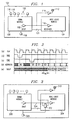
- FIG. 1 is a block diagram of how a single-clock access-time measurement technique that has been applied to an embedded DRAM module.
- DRAM module 100 is integrated on a single semiconductor die 102 with application-specific integrated circuit (ASIC) logic module 104.
- ASIC module 104 may be a microprocessor, microcontroller, digital signal processor, or other logic circuit.
- the clock signal used to regulate the transfer of data into, within, and out of the DRAM is provided at clock terminal 106.
- Buffer driver 108 drives the data out of the DRAM circuit and into the receiver buffer 110 of the ASIC logic module 104.
- the access time measurement is made by sampling the output at data output monitor terminal 112.
- the signal from buffer driver 108 is enhanced by a test buffer driver 114.
- the circuit of Figure 1 suffers from several problems. First, as depicted in Figure 1, it is typical that the receiver buffer 110 of the ASIC logic module 104 is near the middle of the integrated circuit die, while the monitor terminal 112 is near the edge of the die. The distance between the receiver and the monitor terminal 112 causes a signal propagation delay that results in error in the access time measurement. Even more delay in the test signal is induced by the additional driver 114 used to drive the test signal to the test equipment that is coupled to monitor terminal 112.
- Figure 2 is a timing diagram of a synchronous DRAM.
- Signal (a) is an external clock signal applied during testing at terminal 106 in Figure 1, for example.
- Signals (b) and (c) are the complements of the row address and column address strobes, respectively, applied during testing at terminals 116 and 118 in Figure 1, for example.
- Signal (d) is the row and column address information input at a plurality of terminals 120 in Figure 1, for example.
- the DRAM module 100 and ASIC logic module 104 are connected by a bus 121 that carries control and address signals in the operating mode of the integrated circuit where address and control signals are provided to the memory module by the ASIC logic module.
- the signal in line (e) is the data output of the memory circuit.
- the first bits of the output (R0C0) are delayed by three clock cycles, hence the CAS latency is three in this example.
- the delay t AC is the access time of the DRAM. The access time is measured from a rising edge of the clock signal, and is not influenced by a falling clock signal edge.
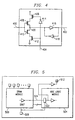
- Figure 3 illustrates a particularly preferred embodiment circuit of the present invention.
- the block diagram of Figure 3 is similar to that of Figure 1, except that storage element or latch 322 is coupled between the output of the DRAM module 300 and the test monitor terminal 312.
- An example of a latch 322 is shown in Figure 4.
- the latch comprises an input terminal 400, an output terminal 402, and a clock terminal 404.
- P-channel transistor 408 and n-channel transistor 410 form an inverter that is enabled or disabled by transistors 406 and 412 in accordance with a clock signal at terminal 404.
- Inverters 416 and 418 form a storage cell or flip-flop core (in this embodiment a cross-coupled inverter storage cell) that stores the output of the inverter formed by transistors 408 and 410 until the output changes.
- the latch may be incorporated in the ASIC logic module 304 or in the DRAM module 300.
- transistors 406 and 412 are conductive and the transistors 408 and 410 act as a conventional inverter.
- a logic high input at terminal 400 produces a logic low output at node 420.
- the output at node 420 is a logic high.
- the signal at node 420 is stored by the storage cell that comprises inverters 416 and 418. The signal is retained by the storage cell until the logic level at node 420 changes.
- Inverter 416 also inverts the signal at node 420 such that a high logic level input at terminal 400, for example, produces a high logic level output at output terminal 402.
- the output terminal 402 remains at the high logic level until a low logic level appears at input terminal 400.
- transistors 406 and 412 are non-conductive, this tri-stating node 420. Therefore, during the low-voltage portion of the clock cycle, the output of the latch remains the same as the last data at the input terminal 400 during the logic high portion of the clock cycle.
- a feature of the latch shown in Figure 4 is that it is made transparent by holding the voltage on the clock terminal 404 at a logic high. In this condition, a signal encounters only slight delay in passing through the latch.
- the latch can also be inactivated when the integrated circuit is in operating mode rather than test mode. By simply holding the clock terminal 404 at a logic low, the transistors 406 and 412 are inactivated, thereby disabling the inverter formed by transistors 408 and 410.
- This feature allows the portions of the integrated circuit of Figure 3 that are associated only with the testing of the circuit to be disabled so as to not interfere with the normal operations of the integrated circuit and to prevent unnecessary dissipation of power in the test circuits.
- the latch occupies a shunt position relative to the memory module output 324.
- the latch is in the data path from the memory module 500 to the ASIC logic module 504. With the clock terminal 404 of the latch held at a logic high, the latch passes the data 524 with only slight delay. Holding the clock terminal low interrupts a data transfer on line 524.
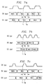
- line (a) is the clock signal supplied at terminal 306 in Figure 3, for example.
- Line (b) is the data output of the DRAM module 300.
- the latch 322 stores the current value of Dout on the falling edge of the clock cycle.
- the data Dout at the falling edge of the clock pulse that begins at t 1 is R0C2.
- the output of the latch 322, Lout reflects the current value at the monitor point t M , of the data output from the memory module 300.
- Figure 7c illustrates that a similar result to that in Figure 7b can be obtained by simply decreasing the duty cycle of the clock pulse while keeping the clock frequency constant.
- the falling edge of the pulse that begins at t 1 occurs with R0C1 is active on line (b), even through the R0C2 data was requested at time t 1 .
- Figures 7a to 7c show a situation where the access times of the memory cell locations R0C0, R0C1 and R0C2 are approximately equal.
- FIGs 7b and 7c all of the Lout data for cell locations R0C0, R0C1 and R0C2 is out of phase with the Dout data for the clock frequency variation shown in Figure 7b and for the clock duty cycle variation shown in Figure 7c.
- all of the latched data for R0C0, R0C1 and R0C2 is out of phase with the Dout data, all of the Dout data is latched. The situation is different when the access times for data locations are substantially different.
- Figures 8a to 8c show a situation where the access times of the memory cell locations are not approximately equal. Specifically, in line (b) of Figure 8a, the access time, t AC1 , of cell R0C2 is much longer than the access time, t AC2 of cell R0C3. At the frequency and duty cycle of the clock signal in line (a), inspection of line (c) shows that all of the data, Dout, in line (b) is latched. A comparison of the phases of the Dout and Lout datastreams however, may not be as valuable as in the situation described in Figures 7a to 7c where the access times of the data cells were relatively uniform.
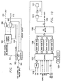
- test circuitry external to the integrated circuit or with built-in self test (BIST) circuitry on the same semiconductor die as the circuit to be tested.
- BIST built-in self test
- the automatic test circuitry 902 is loaded with a data test pattern (alternating 0s and 1s, for example) at terminal 904 so that the tester can expect a particular data output for a particular memory address.
- the test circuitry can generate the test pattern data as needed, rather than retrieve a stored test data pattern as described above.
- the memory circuit 900 is loaded with the same data pattern that is either generated by or loaded into the test circuitry along line 901.
- the frequency of the clock signal on line 906 supplied by the test circuitry to the memory circuit 900 and to the latches 908 associated with each output terminal of the memory circuit is then set to toggle at a frequency low enough to ensure that the falling edge of the clock signal occurs after the access time has elapsed, as in the situation described above in Figure 7a.
- the test circuitry could set the duty cycle of the clock signal to ensure that the falling edge occurs after the access time has elapsed.
- the test circuit reads the Lout data from the latches at terminals 910, it compares that output data to the test pattern loaded prior to the test or to the pattern generated by the test circuit itself.
- the output data should correspond at a given point in the clock cycle (t M ) with the data expected for the addresses chosen by the test circuitry because the access time of the memory circuit is less than the duration of the clock pulse (see Figure 7a).
- the pulse length begins to approach the access time of the memory.
- the Lout data from the latch differs from the Dout data (see Figures 8b and 8c).
- the access time of the memory can them be determined from the pulse width or clock frequency at which the difference in Dout and Lout occurred.
- Figure 10 is a block diagram of a 256 Mb synchronous DRAM having memory cells arranged in four banks 1000. The control and addressing of the DRAM is performed by control circuit block 1002. Latency, burst length, and data output format is controlled by the mode register 1004. In this embodiment, the output 1006 is thirty-two bits wide. The access-time test approach applied in the embodiments above is also applied here. Associated with each of the thirty-two output lines 1008 (shown in Figure 10 as a single line for simplicity) is a latch 1010, and a test terminal 1012.
- a buffer driver 1014 may also be included to enhance the output signals. Only one set of the latch, test terminal, and buffer drive is shown in Figure 10, but it should be noted that each output line is coupled to a similar set of circuit elements.
- the clock signal that controls the operation of the memory circuit at terminal 1016 is coupled by line 1018 to latch 1010 to synchronize the latching of output data with memory operation. The access time test is performed as described above with reference to the embedded memory circuit.
Landscapes
- For Increasing The Reliability Of Semiconductor Memories (AREA)
- Techniques For Improving Reliability Of Storages (AREA)
- Tests Of Electronic Circuits (AREA)
- Dram (AREA)
- Test And Diagnosis Of Digital Computers (AREA)
Applications Claiming Priority (2)
| Application Number | Priority Date | Filing Date | Title |
|---|---|---|---|
| US4109197P | 1997-03-14 | 1997-03-14 | |
| US41091P | 1997-03-14 |
Publications (2)
| Publication Number | Publication Date |
|---|---|
| EP0867887A2 true EP0867887A2 (de) | 1998-09-30 |
| EP0867887A3 EP0867887A3 (de) | 1998-11-25 |
Family
ID=21914684
Family Applications (1)
| Application Number | Title | Priority Date | Filing Date |
|---|---|---|---|
| EP98103271A Withdrawn EP0867887A3 (de) | 1997-03-14 | 1998-02-25 | Verfahren und Anordnung zur Messung von Speicherzugriffszeit |
Country Status (3)
| Country | Link |
|---|---|
| US (1) | US6266749B1 (de) |
| EP (1) | EP0867887A3 (de) |
| JP (1) | JPH10255498A (de) |
Cited By (9)
| Publication number | Priority date | Publication date | Assignee | Title |
|---|---|---|---|---|
| EP0892404A2 (de) * | 1997-07-16 | 1999-01-20 | Victor Company Of Japan, Limited | Aufzeichnungsmedium und Audiosignalverarbeitungsgerät |
| EP0898284A2 (de) * | 1997-07-31 | 1999-02-24 | Nec Corporation | Halbleiterspeicher mit einer Prüfschaltung |
| EP1052648A1 (de) * | 1999-05-11 | 2000-11-15 | STMicroelectronics Limited | Antwortzeitmessung |
| EP1061528A1 (de) * | 1999-06-16 | 2000-12-20 | STMicroelectronics Limited | Speicherprüfung |
| EP1094471A2 (de) * | 1999-10-21 | 2001-04-25 | Softlink | Verfahren zur Prüfung von elektronischen Bauteilen |
| WO2002103706A2 (en) * | 2001-06-15 | 2002-12-27 | Artisan Components, Inc. | System and method for identification of faulty or weak memory cells under simulated extreme operating conditions |
| WO2005088644A1 (en) * | 2004-03-05 | 2005-09-22 | Koninklijke Philips Electronics N.V. | Dft technique for stressing self-timed semiconductor memories to detect delay faults |
| CN107705818A (zh) * | 2016-08-08 | 2018-02-16 | 中芯国际集成电路制造(上海)有限公司 | 一种访问时间测量电路和访问时间测量方法 |
| CN107785041A (zh) * | 2016-08-26 | 2018-03-09 | Arm 有限公司 | 存储电路和数据处理系统 |
Families Citing this family (14)
| Publication number | Priority date | Publication date | Assignee | Title |
|---|---|---|---|---|
| US6519716B1 (en) * | 1999-09-22 | 2003-02-11 | International Business Machines Corporation | Electronic device initialization with dynamic selection of access time for non-volatile memory |
| JP4480238B2 (ja) * | 2000-07-18 | 2010-06-16 | Okiセミコンダクタ株式会社 | 半導体装置 |
| US6424583B1 (en) * | 2000-11-30 | 2002-07-23 | Taiwan Semiconductor Manufacturing Co., Ltd | System and measuring access time of embedded memories |
| US20040024941A1 (en) * | 2002-07-31 | 2004-02-05 | Compaq Information Technologies Group, L.P. | Method and apparatus for supporting hot-plug cache memory |
| US7210078B2 (en) * | 2002-08-29 | 2007-04-24 | Texas Instruments Incorporated | Error bit method and circuitry for oscillation-based characterization |
| TWI229343B (en) * | 2002-11-27 | 2005-03-11 | Univ Tsinghua | Embedded memory access time measurement method and device |
| US7461304B1 (en) * | 2003-07-07 | 2008-12-02 | Marvell Israel (M.I.S.L.) Ltd. | Integrated circuit test using clock signal modification |
| DE602004007349T2 (de) * | 2004-01-15 | 2008-03-13 | Infineon Technologies Ag | Vorrichtung zur Bestimmung der Zugriffszeit und/oder der minimalen Zykluszeit eines Speichers |
| EP2286412A1 (de) | 2007-12-21 | 2011-02-23 | Rambus Inc. | Flash-speicher-timing-vorcharakterisierung zur verwendung beim ormal-betrieb |
| US8214699B2 (en) * | 2008-06-27 | 2012-07-03 | International Business Machines Corporation | Circuit structure and method for digital integrated circuit performance screening |
| US8707001B2 (en) * | 2008-12-04 | 2014-04-22 | Qualcomm Incorporated | Method and system for measuring memory access time using phase detector |
| US8212700B2 (en) * | 2009-07-09 | 2012-07-03 | Stellamar Llc | Delta-sigma-delta modulator |
| US8627155B1 (en) * | 2010-03-09 | 2014-01-07 | Marvell International Ltd. | Integrated circuit testing with clock manipulation and auto-step features |
| US9753086B2 (en) | 2014-10-02 | 2017-09-05 | Samsung Electronics Co., Ltd. | Scan flip-flop and scan test circuit including the same |
Citations (3)
| Publication number | Priority date | Publication date | Assignee | Title |
|---|---|---|---|---|
| DE3700251A1 (de) * | 1986-01-07 | 1987-07-09 | Hitachi Ltd | Verfahren und vorrichtung zur diagnose logischer schaltungen |
| EP0260982A2 (de) * | 1986-09-19 | 1988-03-23 | Fujitsu Limited | Prüfsystem für Direktzugriffsspeicher |
| US4965799A (en) * | 1988-08-05 | 1990-10-23 | Microcomputer Doctors, Inc. | Method and apparatus for testing integrated circuit memories |
Family Cites Families (8)
| Publication number | Priority date | Publication date | Assignee | Title |
|---|---|---|---|---|
| JPS647400A (en) * | 1987-06-29 | 1989-01-11 | Hitachi Ltd | Ic tester |
| US5289475A (en) * | 1990-11-29 | 1994-02-22 | Sgs-Thomson Microelectronics, Inc. | Semiconductor memory with inverted write-back capability and method of testing a memory using inverted write-back |
| EP0632384A1 (de) * | 1993-06-30 | 1995-01-04 | International Business Machines Corporation | Programmierbare hochgeschwindigkeitstaktgeberschaltung für Halbleiterspeicherchip mit eingebautem Selbsttest |
| US5640527A (en) * | 1993-07-14 | 1997-06-17 | Dell Usa, L.P. | Apparatus and method for address pipelining of dynamic random access memory utilizing transparent page address latches to reduce wait states |
| JP3753190B2 (ja) * | 1995-04-26 | 2006-03-08 | 三菱電機株式会社 | 半導体装置 |
| US5664166A (en) * | 1995-05-10 | 1997-09-02 | 3Comcorporation | System for generating a variable signal in response to a toggle signal selectively delayed using a clock edge and time delay measured from the clock edge |
| US5555209A (en) * | 1995-08-02 | 1996-09-10 | Simple Technology, Inc. | Circuit for latching data signals from DRAM memory |
| US6081783A (en) * | 1997-11-14 | 2000-06-27 | Cirrus Logic, Inc. | Dual processor digital audio decoder with shared memory data transfer and task partitioning for decompressing compressed audio data, and systems and methods using the same |
-
1998
- 1998-02-25 EP EP98103271A patent/EP0867887A3/de not_active Withdrawn
- 1998-03-12 US US09/041,264 patent/US6266749B1/en not_active Expired - Lifetime
- 1998-03-13 JP JP10063147A patent/JPH10255498A/ja active Pending
Patent Citations (3)
| Publication number | Priority date | Publication date | Assignee | Title |
|---|---|---|---|---|
| DE3700251A1 (de) * | 1986-01-07 | 1987-07-09 | Hitachi Ltd | Verfahren und vorrichtung zur diagnose logischer schaltungen |
| EP0260982A2 (de) * | 1986-09-19 | 1988-03-23 | Fujitsu Limited | Prüfsystem für Direktzugriffsspeicher |
| US4965799A (en) * | 1988-08-05 | 1990-10-23 | Microcomputer Doctors, Inc. | Method and apparatus for testing integrated circuit memories |
Cited By (28)
| Publication number | Priority date | Publication date | Assignee | Title |
|---|---|---|---|---|
| US7006422B2 (en) | 1997-07-16 | 2006-02-28 | Victor Company Of Japan, Ltd. | Recording medium and audio-signal processing apparatus |
| US7398011B2 (en) | 1997-07-16 | 2008-07-08 | Victor Company Of Japan, Ltd. | Recording medium and audio-signal processing apparatus |
| US7379413B2 (en) | 1997-07-16 | 2008-05-27 | Victor Company Of Japan, Ltd. | Recording medium and audio-signal processing apparatus |
| US7123575B2 (en) | 1997-07-16 | 2006-10-17 | Victor Company Of Japan, Ltd. | Recording medium and audio-signal processing apparatus |
| EP0892404A2 (de) * | 1997-07-16 | 1999-01-20 | Victor Company Of Japan, Limited | Aufzeichnungsmedium und Audiosignalverarbeitungsgerät |
| US6980501B2 (en) | 1997-07-16 | 2005-12-27 | Victor Company Of Japan, Ltd. | Recording medium and audio-signal processing apparatus |
| EP0892404A3 (de) * | 1997-07-16 | 2002-01-16 | Victor Company Of Japan, Limited | Aufzeichnungsmedium und Audiosignalverarbeitungsgerät |
| US6636474B1 (en) | 1997-07-16 | 2003-10-21 | Victor Company Of Japan, Ltd. | Recording medium and audio-signal processing apparatus |
| US6810003B2 (en) | 1997-07-16 | 2004-10-26 | Victor Company Of Japan, Ltd. | Recording medium and audio-signal processing apparatus |
| EP0898284A3 (de) * | 1997-07-31 | 1999-09-15 | Nec Corporation | Halbleiterspeicher mit einer Prüfschaltung |
| EP0898284A2 (de) * | 1997-07-31 | 1999-02-24 | Nec Corporation | Halbleiterspeicher mit einer Prüfschaltung |
| US6584577B1 (en) | 1999-05-11 | 2003-06-24 | Stmicroelectronics Limited | System for measuring response time of a circuit by determining the time difference between the earlier and the later clock pulses applied to the circuit |
| EP1052648A1 (de) * | 1999-05-11 | 2000-11-15 | STMicroelectronics Limited | Antwortzeitmessung |
| US6604213B1 (en) | 1999-06-16 | 2003-08-05 | Stmicroelectronics Limited | Method and apparatus for determining a minimum clock delay in a memory |
| EP1061528A1 (de) * | 1999-06-16 | 2000-12-20 | STMicroelectronics Limited | Speicherprüfung |
| US6813740B1 (en) | 1999-10-21 | 2004-11-02 | Softlink | Method for the testing of electronic components |
| SG93276A1 (en) * | 1999-10-21 | 2002-12-17 | Softlink | Method for the testing of electronic components |
| EP1094471A3 (de) * | 1999-10-21 | 2001-12-19 | Softlink | Verfahren zur Prüfung von elektronischen Bauteilen |
| FR2800168A1 (fr) * | 1999-10-21 | 2001-04-27 | Softlink | Procede de test de composants electroniques |
| EP1094471A2 (de) * | 1999-10-21 | 2001-04-25 | Softlink | Verfahren zur Prüfung von elektronischen Bauteilen |
| WO2002103706A3 (en) * | 2001-06-15 | 2003-08-28 | Artisan Components Inc | System and method for identification of faulty or weak memory cells under simulated extreme operating conditions |
| US6862721B2 (en) | 2001-06-15 | 2005-03-01 | Artisan Components, Inc. | Method for identification of faulty or weak functional logic elements under simulated extreme operating conditions |
| US6667917B1 (en) | 2001-06-15 | 2003-12-23 | Artisan Components, Inc. | System and method for identification of faulty or weak memory cells under simulated extreme operating conditions |
| WO2002103706A2 (en) * | 2001-06-15 | 2002-12-27 | Artisan Components, Inc. | System and method for identification of faulty or weak memory cells under simulated extreme operating conditions |
| WO2005088644A1 (en) * | 2004-03-05 | 2005-09-22 | Koninklijke Philips Electronics N.V. | Dft technique for stressing self-timed semiconductor memories to detect delay faults |
| CN107705818A (zh) * | 2016-08-08 | 2018-02-16 | 中芯国际集成电路制造(上海)有限公司 | 一种访问时间测量电路和访问时间测量方法 |
| CN107785041A (zh) * | 2016-08-26 | 2018-03-09 | Arm 有限公司 | 存储电路和数据处理系统 |
| CN107785041B (zh) * | 2016-08-26 | 2023-06-16 | Arm 有限公司 | 存储电路和数据处理系统 |
Also Published As
| Publication number | Publication date |
|---|---|
| JPH10255498A (ja) | 1998-09-25 |
| EP0867887A3 (de) | 1998-11-25 |
| US6266749B1 (en) | 2001-07-24 |
Similar Documents
| Publication | Publication Date | Title |
|---|---|---|
| EP0867887A2 (de) | Verfahren und Anordnung zur Messung von Speicherzugriffszeit | |
| KR0137756B1 (ko) | 동기형 다이나믹 ram | |
| US7573778B2 (en) | Semiconductor memory device | |
| US6324118B1 (en) | Synchronous semiconductor memory device having improved operational frequency margin at data input/output | |
| KR100508196B1 (ko) | Sdram 클럭킹 테스트 모드 | |
| US6338127B1 (en) | Method and apparatus for resynchronizing a plurality of clock signals used to latch respective digital signals, and memory device using same | |
| KR20010067326A (ko) | 자기 시험 회로 및 이 자기 시험 회로를 내장한 메모리디바이스 | |
| US20100052727A1 (en) | Synchronous semiconductor device, and inspection system and method for the same | |
| JPS60245275A (ja) | メモリ・アレイ・チツプ | |
| EP0567104A2 (de) | Schaltung zur Erkennung von Auffrischungadressignalen eines Halbleiterspeichersgeräts | |
| EP0895245B1 (de) | Synchrone Halbleiterspeicheranordnung | |
| US6807116B2 (en) | Semiconductor circuit device capable of accurately testing embedded memory | |
| KR100546538B1 (ko) | 시험 시간을 단축시키기 위한 내부 클럭 증대 | |
| US20040051548A1 (en) | Semiconductor integrated circuit having a semiconductor storage circuit and a test circuit for testing the semiconductor storage circuit | |
| KR19990047220A (ko) | 직접 억세스 모드 테스트를 사용하는 메모리 장치 및 테스트방법 | |
| KR20080005294A (ko) | 라이브 측정으로 측정-초기화되는 지연 고정 루프 | |
| EP0325105A1 (de) | Multiport-Speicher | |
| KR0154741B1 (ko) | 듀얼포트 메모리 장치 및 듀얼포트 메모리 장치의 시리얼데이타 출력방법 | |
| US6317373B1 (en) | Semiconductor memory device having a test mode and semiconductor testing method utilizing the same | |
| US20040217795A1 (en) | Delay adjusting apparatus providing different delay times by producing a plurality of delay control signals | |
| JPH10132908A (ja) | 半導体装置および半導体装置の内部機能識別方法 | |
| US6158029A (en) | Method of testing an integrated circuit having a memory and a test circuit | |
| US6643217B2 (en) | Semiconductor memory device permitting early detection of defective test data | |
| EP0416532A2 (de) | Halbleiterspeichergerät, das mit "scan-path" diagnostischem Modusbetrieb versehenen peripheren Logik-Gattern verbunden ist | |
| US6115783A (en) | Integrated circuit |
Legal Events
| Date | Code | Title | Description |
|---|---|---|---|
| PUAI | Public reference made under article 153(3) epc to a published international application that has entered the european phase |
Free format text: ORIGINAL CODE: 0009012 |
|
| AK | Designated contracting states |
Kind code of ref document: A2 Designated state(s): DE FR GB IT NL |
|
| AX | Request for extension of the european patent |
Free format text: AL;LT;LV;MK;RO;SI |
|
| PUAL | Search report despatched |
Free format text: ORIGINAL CODE: 0009013 |
|
| AK | Designated contracting states |
Kind code of ref document: A3 Designated state(s): AT BE CH DE DK ES FI FR GB GR IE IT LI LU MC NL PT SE |
|
| AX | Request for extension of the european patent |
Free format text: AL;LT;LV;MK;RO;SI |
|
| 17P | Request for examination filed |
Effective date: 19990519 |
|
| AKX | Designation fees paid |
Free format text: DE FR GB IT NL |
|
| 17Q | First examination report despatched |
Effective date: 20030116 |
|
| STAA | Information on the status of an ep patent application or granted ep patent |
Free format text: STATUS: THE APPLICATION IS DEEMED TO BE WITHDRAWN |
|
| 18D | Application deemed to be withdrawn |
Effective date: 20030527 |