EP0862126A2 - Simulationsvorrichtung für ein Ionenimplantationsverfahren zur Realisierung einer genauen Interpolation von Ionenimplantationsprofilen und Simulationsverfahren - Google Patents
Simulationsvorrichtung für ein Ionenimplantationsverfahren zur Realisierung einer genauen Interpolation von Ionenimplantationsprofilen und Simulationsverfahren Download PDFInfo
- Publication number
- EP0862126A2 EP0862126A2 EP98103392A EP98103392A EP0862126A2 EP 0862126 A2 EP0862126 A2 EP 0862126A2 EP 98103392 A EP98103392 A EP 98103392A EP 98103392 A EP98103392 A EP 98103392A EP 0862126 A2 EP0862126 A2 EP 0862126A2
- Authority
- EP
- European Patent Office
- Prior art keywords
- dose
- ion implantation
- logd
- coefficient
- sub
- Prior art date
- Legal status (The legal status is an assumption and is not a legal conclusion. Google has not performed a legal analysis and makes no representation as to the accuracy of the status listed.)
- Withdrawn
Links
Images


Classifications
-
- H10P34/00—
-
- G—PHYSICS
- G06—COMPUTING OR CALCULATING; COUNTING
- G06F—ELECTRIC DIGITAL DATA PROCESSING
- G06F30/00—Computer-aided design [CAD]
- G06F30/20—Design optimisation, verification or simulation
- G06F30/23—Design optimisation, verification or simulation using finite element methods [FEM] or finite difference methods [FDM]
Definitions
- the present invention relates to an ion implantation process simulation device realizing accurate interpolation and extrapolation of ion implantation profiles including tails in ion implantation process simulation for a semiconductor device, and a simulation method therefor.
- a manufacturing process of semiconductor devices including LSI includes a step of implanting impurity ions as dopant into a semiconductor substrate by an ion implantation technique and diffusing and activating them through a thermal treatment. It is well-known that an impurity distribution obtained in this step accounts for the considerable change in a threshold voltage Vt, an ON-state current of a transistor and other electrical characteristics parameters. In recent years, in particular, for reducing a semiconductor in size to achieve high density large capacity and high speed, designing a transistor with shallower junctions has been gaining more importance. More specifically, demanded is not only accurate control of a peak concentration of impurities but also accurate adjustment of position of the tail of an ion implantation profile.
- ion implantation process simulation using a computer is adopted. This is a method of predicting and calculating various ion implantation profiles for use in manufacturing semiconductor devices by using predetermined models and algorithms on a computer. Use of ion implantation process simulation largely contributes to the reduction in the number of experimental steps for improving element characteristics of a semiconductor device and to the improvement in efficiency of designing work.
- ion implantation profiles are described using a Gaussian or Pearson function which can obtain satisfactory enough approximation when crystals are amorphous.
- profiles will vary depending on crystal orientation of the substrate and an ion implantation angle, that is, the channeling phenomenon will occur.
- the channeling phenomenon tends to decrease with an increase in dose value. This is because crystals become amorphous as a dose value is increased.
- Profiles of ion implantation into a semiconductor crystal substrate can not therefore be described by using a simple Gaussian or Pearson function but can be described by using a plurality of functions.
- a technique of describing a profile of ion implantation into a semiconductor crystal substrate by using a function and simulating the same is disclosed, for example, in "An Improved Approach to Accurately Model Shallow B and BF 2 Implants in Silicon” (Al F. Tasch, H. Shin, and C. Park; J. Electrochem. Soc., Vol. 136, No. 3, March 1989, pp. 810-814; The Electrochemical Society, Inc.).
- the literature recites a method of more accurately simulating experimental profiles of as-implanted ion impurities.
- the experimental profiles are results of measurement obtained by the SIMS (Secondary Ion Mass Spectrometry) method.
- SIMS is a well-known method of irradiating a surface region of a semiconductor with a primary ion such as an oxygen ion or a cesium ion to generate a secondary ion and conducting mass analysis of the secondary ion to measure an impurity distribution.
- the experimentally obtained ion implantation profile is expressed using two Pearson functions which represent an amorphous component and a channeling component, respectively.
- the ion implantation profile N(x) is described as a sum of the two components as shown in the following equation (1).
- N(x) D main f main (x)+D sub f sub (x)
- a main peak amorphous component function f main (x) and a subsidiary peak channeling component function f sub (x) are normalized functions not dependent on a dose value
- D main represents a main peak amorphous component dose coefficient
- D sub represents a subsidiary peak channeling component dose coefficient.
- a total dose D T of the ion implantation profile N(x) is described as a sum of coefficients of the amorphous component dose and the channeling component dose as shown in the following equation (2).
- D T ⁇ 0 ⁇ N(x)dx D main + D sub
- the Pearson function used here is described using four kinds of moment parameters, projected range Rp, standard deviation ⁇ Rp, skewness ⁇ and kurtosis ⁇ .
- a conventional ion implantation process simulation method of obtaining an ion implantation profile for a prescribed dose by interpolation with reference to a flow chart of Fig. 6.
- Fig. 6 first, from table data of ion implantation profiles for several dose values, extract moment parameters, projected range Rp, standard deviation ⁇ Rp, skewness ⁇ and kurtosis ⁇ in two normalized functions respectively representing the amorphous component and the channeling component (moment parameters of a Dual Pearson function), an amorphous component dose coefficient and a channeling component dose coefficient (Step 601).
- a Dual Pearson data table is prepared.
- Step 602 select parameters for doses at two points most neighboring to an arbitrary dose from the Dual Pearson data table (Step 602).
- Step 603 linearly interpolate the dose-dependent amorphous component dose coefficient and channeling component dose efficient with respect to dose (Step 603).
- Fig. 7 is a diagram showing a dose dependency as a parameter to be interpolated.
- the abscissa represents a dose value
- the ordinate represents a main peak amorphous component dose ratio
- the polygonal line represents a dose dependency of a main peak amorphous component dose ratio.
- the number of dose points of the experimental data shown in the diagram are five, not so many. Ratios of the coefficients of a main peak amorphous component dose to the total dose at the other doses need to be interpolated for all the doses.
- the curve CP3 of the profile N a (x) obtained by linear interpolation between the profile curves CP2 and CP4 according to the above-described conventional linear interpolation method crosses with the profile curves CP1 and CP2 for larger doses at the tail.
- the profile curve CP3 is undesirably shown to have a higher concentration than those of the profile curves CP1 and CP2.
- An object of the present invention is to provide an ion implantation process simulation device which accurately interpolates and extrapolates ion implantation profiles for a semiconductor device covering tails and a simulation method therefor.
- an ion implantation process simulation device which conducts ion implantation process simulation for a semiconductor device to conduct interpolation and extrapolation necessary for an ion implantation profile, comprises
- said dose coefficient interpolating/extrapolating means when an experimentally extracted moment parameter is dependent on a dose value, further interpolates and extrapolates said dose-dependent moment parameter with respect to logarithmic values of all doses.
- an ion implantation process simulation method of conducting ion implantation process simulation for a semiconductor device to conduct interpolation and extrapolation necessary for an ion implantation profile comprising the steps of:
- said dose coefficient interpolating/extrapolating step further comprises the step of, when an experimentally extracted moment parameter is dependent on a dose value, interpolating and extrapolating said dose-dependent moment parameter with respect to logarithmic values of all doses.
- an ion implantation process simulation method of conducting ion implantation process simulation for a semiconductor device to conduct interpolation and extrapolation necessary for an ion implantation profile comprising the steps of:
- a channeling component dose coefficient for the arbitrary dose value is interpolated and extrapolated by using said amorphous component dose coefficients and channeling component dose coefficients at dose values of two points most neighboring to the dose value.
- an ion implantation process simulation method of conducting ion implantation process simulation for a semiconductor device to conduct interpolation and extrapolation necessary for an ion implantation profile comprising the steps of:
- a computer readable memory having a control program for controlling an ion implantation process simulation device to conduct ion implantation process simulation for a semiconductor device and conduct interpolation and extrapolation necessary for an ion implantation profile, said control program comprising the steps of:
- Fig. 1 is a block diagram showing structure of an ion implantation process simulation device according to one embodiment of the present invention.
- the ion implantation process simulation device of the present embodiment is implemented by a computer system such as a work station or a personal computer, and functions of the present embodiment which will be described in the following are executed by a control program which controls the computer system.
- the control program is provided as storage in a storage medium such as a magnetic disk or a semiconductor memory and load of the control program into a processing device of the computer system realizes the ion implantation process simulation device of the present embodiment.
- the ion implantation process simulation device of the present invention includes a Dual Pearson data extracting unit 10 for extracting desired Dual Pearson data from ion implantation profile data 50 to generate a Dual Pearson data table 11, a Dual Pearson data for interpolation obtaining unit 20 for obtaining Dual Pearson parameters for use in interpolating and extrapolating dose coefficients from the Dual Pearson data table 11 generated by the Dual Pearson data extracting unit 10, a dose coefficient interpolating/extrapolating unit 30 for interpolating or extrapolating dose coefficients by using a parameter obtained by the Dual Pearson data for interpolation obtaining unit 20, and a simulation result outputting unit 40 for outputting a simulation result obtained by interpolation of dose coefficients.
- illustration is made only of a characteristic part of the structure of the present embodiment and that of the remaining common part is omitted.
- the Dual Pearson data extracting unit 10 receives input of the ion implantation profile data 50 for various dose values to generate the Dual Pearson data table 11 in advance.
- Stored in the Dual Pearson data table 11 are moment parameters, projected range Rp, standard deviation ⁇ Rp, skewness ⁇ and kurtosis ⁇ in two normalized functions respectively representing an amorphous component and a channeling component (moment parameters of a Dual Pearson function), an amorphous component dose coefficient and a channeling component dose coefficient.
- the Dual Pearson data for interpolation obtaining unit 20 obtains parameters at dose values of two points most neighboring to an arbitrary dose designated by a designation means not shown (hereinafter referred to as a Dual Pearson parameter) from the Dual Pearson data table 11.
- the dose coefficient interpolating/extrapolating unit 30 when out of the Dual Pearson parameters obtained by the Dual Pearson data for interpolation obtaining unit 20, an amorphous component dose coefficient and a channeling component dose coefficient are dependent on a dose value, interpolates or extrapolates the amorphous component dose coefficient and the channeling component dose coefficient with respect to all the dose values in the following manner.
- the dose coefficient interpolating/extrapolating unit 30 first uses two normalized functions respectively representing the amorphous component and the channeling component, and an amorphous component dose coefficient and a channeling component dose coefficient corresponding to the two functions to express a profile of ion implantation into a semiconductor crystal substrate as linear connection of the two functions. Then, at the time of describing an ion implantation profile for a dose value designated by a user, the unit 30 uses dose-independent moment parameters extracted from the ion implantation profile and coefficients of the linear connection dependent on dose at a plurality of dose values to interpolate or extrapolate a logarithmic value of a channeling component dose coefficient with respect to logarithmic values of all the dose values.
- the simulation result outputting unit 40 generates such a profile diagram as shown in Fig. 3 by using a simulation result obtained by the interpolation and extrapolation by the dose coefficient interpolating/extrapolating unit 30 and displays the same on a display device or prints out the same.
- the Dual Pearson data extracting unit 10 first extracts moment parameters, an amorphous component dose coefficient and a channeling component dose coefficient of a Dual Pearson function from the ion implantation profile data 50 for several dose values to generate the Dual Pearson data table 11 (Step 201).
- the Dual Pearson data for interpolation obtaining unit 20 obtains Dual Pearson parameters for dose values at two points most neighboring to an arbitrary dose designated by a designation means not shown from the Dual Pearson data table 11 (Step 202).
- the dose coefficient interpolating/extrapolating unit 30 determines whether out of the Dual Pearson parameters obtained by the Dual Pearson data for interpolation obtaining unit 20, an amorphous component dose coefficient and a channeling component dose coefficient are dependent on a dose value or not and when the determination is made that they are dose dependent, interpolates or extrapolates the amorphous component dose coefficient and the channeling component dose coefficient with respect to the dose value in question in the above-described manner (Step 203).
- the simulation result outputting unit 40 Based on the calculation results of ion implantation profiles thus obtained by interpolation and extrapolation of dose coefficients, the simulation result outputting unit 40 generates and outputs a profile diagram.
- Fig. 3 shows calculation results of ion implantation profiles for BF 2 according to the present embodiment.
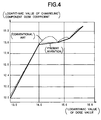
- Fig. 4 is a diagram showing a channeling component dose coefficient as compared with that of conventional simulation.
- the solid line denotes a relationship between a logarithmic value of a channeling component dose coefficient and a logarithmic value of all dose values in the simulation according to the present embodiment
- the broken line denotes a relationship between a logarithmic value of a channeling component dose coefficient and a logarithmic value of all dose values in conventional simulation.
- a rugged part appears in the conventional simulation as indicated by the broken line, while in the simulation according to the present embodiment, the relationship shows monotonic increase as indicated by the solid line.
- the present embodiment enables accurate interpolation of ion implantation profiles including tails which is demanded in simulation for a junction depth crucial to the manufacture of semiconductor devices.
- the dose coefficient interpolating/extrapolating unit 30 similarly to the first embodiment, interpolates or extrapolates an amorphous component dose coefficient and a channeling component dose coefficient with respect to a dose value, and also determines whether out of Dual Pearson parameters, moment parameters of a Dual Pearson function for dose values at two points most neighboring to a dose value to be calculated are dose dependent and when the determination is made that they are dose dependent, interpolates or extrapolates the moment parameters of the Dual Pearson function with respect to a dose in a manner set forth in the following.
- the unit 30 interpolates or extrapolates the above-described dose-dependent moment parameters with respect to a logarithmic value of all doses.
- Fig. 5 is a flow chart showing another example of operation of the present embodiment.
- operation at Steps 501 to 503 by the dose coefficient interpolating/extrapolating unit 30 is the same as that at Steps 201 to 203 of the operation example shown in Fig. 3.
- the dose coefficient interpolating/extrapolating unit 30 determines whether out of the Dual Pearson parameters, moment parameters of a Dual Pearson function for dose values at two points most neighboring to a dose value to be calculated are dose dependent and when they are dependent, interpolates or extrapolates the moment parameters of the Dual Pearson function with respect to a dose in the following manner (Steps 504 and 505).
- skewness ⁇ is a dose-dependent parameter.
- profile curves might cross with each other at tails in some cases, while the present invention enables accurate profiles to be obtained in which none of profile curves crosses with each other at tails.
- the present invention enables accurate interpolation and extrapolation of ion implantation profiles including tails.
Landscapes
- Engineering & Computer Science (AREA)
- Physics & Mathematics (AREA)
- Theoretical Computer Science (AREA)
- Computer Hardware Design (AREA)
- Evolutionary Computation (AREA)
- Geometry (AREA)
- General Engineering & Computer Science (AREA)
- General Physics & Mathematics (AREA)
- Management, Administration, Business Operations System, And Electronic Commerce (AREA)
Applications Claiming Priority (3)
| Application Number | Priority Date | Filing Date | Title |
|---|---|---|---|
| JP44030/97 | 1997-02-27 | ||
| JP09044030A JP3102372B2 (ja) | 1997-02-27 | 1997-02-27 | イオン注入プロセスシミュレーション方法 |
| JP4403097 | 1997-02-27 |
Publications (2)
| Publication Number | Publication Date |
|---|---|
| EP0862126A2 true EP0862126A2 (de) | 1998-09-02 |
| EP0862126A3 EP0862126A3 (de) | 2000-02-23 |
Family
ID=12680252
Family Applications (1)
| Application Number | Title | Priority Date | Filing Date |
|---|---|---|---|
| EP98103392A Withdrawn EP0862126A3 (de) | 1997-02-27 | 1998-02-26 | Simulationsvorrichtung für ein Ionenimplantationsverfahren zur Realisierung einer genauen Interpolation von Ionenimplantationsprofilen und Simulationsverfahren |
Country Status (5)
| Country | Link |
|---|---|
| US (1) | US5999719A (de) |
| EP (1) | EP0862126A3 (de) |
| JP (1) | JP3102372B2 (de) |
| KR (1) | KR100291815B1 (de) |
| CN (1) | CN1195881A (de) |
Cited By (1)
| Publication number | Priority date | Publication date | Assignee | Title |
|---|---|---|---|---|
| US7142297B2 (en) | 2003-10-31 | 2006-11-28 | Synopsys Switzerland Llc | Method for simulating the movement of particles |
Families Citing this family (15)
| Publication number | Priority date | Publication date | Assignee | Title |
|---|---|---|---|---|
| JP3228220B2 (ja) * | 1998-05-15 | 2001-11-12 | 日本電気株式会社 | イオン注入シミュレーション方法 |
| KR100642590B1 (ko) * | 1999-11-06 | 2006-11-03 | 원태영 | 효율적인 계산 시간을 갖는 3차원 이온주입 수치해석 방법 |
| JP4991062B2 (ja) * | 2001-05-29 | 2012-08-01 | ラピスセミコンダクタ株式会社 | 半導体プロセスデバイスモデリング方法 |
| US6677168B1 (en) * | 2002-04-30 | 2004-01-13 | Advanced Micro Devices, Inc. | Analysis of ion implant dosage |
| JP4641144B2 (ja) * | 2003-08-01 | 2011-03-02 | 富士通株式会社 | イオン注入の不純物濃度分布用パラメータにおける多階層構造のデータベース及びそれのデータ抽出プログラム |
| CN1322552C (zh) * | 2003-08-19 | 2007-06-20 | 北京大学 | 离子注入涨落的模拟方法 |
| JP2005093802A (ja) * | 2003-09-18 | 2005-04-07 | Oki Electric Ind Co Ltd | Esd保護素子のモデル化方法,esdシミュレーション方法 |
| JP4983601B2 (ja) * | 2005-07-13 | 2012-07-25 | 富士通株式会社 | イオン注入のシミュレーション方法及び半導体装置の製造方法 |
| CN100428413C (zh) * | 2006-05-22 | 2008-10-22 | 中芯国际集成电路制造(上海)有限公司 | 离子注入模拟方法 |
| US7935618B2 (en) | 2007-09-26 | 2011-05-03 | Micron Technology, Inc. | Sputtering-less ultra-low energy ion implantation |
| JP5277668B2 (ja) * | 2008-03-10 | 2013-08-28 | 富士通株式会社 | イオン注入分布発生方法 |
| JP5821163B2 (ja) * | 2010-04-20 | 2015-11-24 | 富士通株式会社 | イオン注入条件設定方法、プロセス・デバイスシミュレータ、記憶媒体、及びプログラム |
| KR101878734B1 (ko) * | 2011-06-24 | 2018-07-16 | 삼성전자주식회사 | 그래핀 층상 구조체, 그의 제조방법 및 이를 채용한 투명전극과 트랜지스터 |
| CN103927415B (zh) * | 2014-04-08 | 2017-07-11 | 上海华力微电子有限公司 | 离子注入浓度的校准方法 |
| KR20240142165A (ko) | 2023-03-21 | 2024-09-30 | (주)동아시스템 | 공장 자동화 설비 및 공정의 시뮬레이션 장치 및 방법 |
Family Cites Families (4)
| Publication number | Priority date | Publication date | Assignee | Title |
|---|---|---|---|---|
| JPH08279446A (ja) * | 1995-04-07 | 1996-10-22 | Mitsubishi Electric Corp | 半導体装置の製造方法 |
| JP2716009B2 (ja) * | 1995-07-28 | 1998-02-18 | 日本電気株式会社 | 欠陥分布シミュレーション方法 |
| US5719796A (en) * | 1995-12-04 | 1998-02-17 | Advanced Micro Devices, Inc. | System for monitoring and analyzing manufacturing processes using statistical simulation with single step feedback |
| JP4286924B2 (ja) * | 1997-04-18 | 2009-07-01 | 株式会社東芝 | 半導体装置の製造方法、半導体装置の特性評価装置、半導体装置の特性評価方法、及び、半導体装置の特性評価プログラムを記録した機械読み取り可能な記録媒体 |
-
1997
- 1997-02-27 JP JP09044030A patent/JP3102372B2/ja not_active Expired - Fee Related
-
1998
- 1998-02-26 US US09/030,774 patent/US5999719A/en not_active Expired - Fee Related
- 1998-02-26 EP EP98103392A patent/EP0862126A3/de not_active Withdrawn
- 1998-02-27 CN CN98100467A patent/CN1195881A/zh active Pending
- 1998-02-27 KR KR1019980006452A patent/KR100291815B1/ko not_active Expired - Fee Related
Non-Patent Citations (1)
| Title |
|---|
| PARK C ET AL: "Efficient modeling parameter extraction for dual Pearson approach to simulation of implanted impurity profiles in silicon" SOLID-STATE ELECTRONICS, JUNE 1990, UK, vol. 33, no. 6, pages 645-650, XP000857525 ISSN: 0038-1101 * |
Cited By (2)
| Publication number | Priority date | Publication date | Assignee | Title |
|---|---|---|---|---|
| US7142297B2 (en) | 2003-10-31 | 2006-11-28 | Synopsys Switzerland Llc | Method for simulating the movement of particles |
| US7538873B2 (en) | 2003-10-31 | 2009-05-26 | Synopsys Switzerland Llc | Method for simulating the movement of particles |
Also Published As
| Publication number | Publication date |
|---|---|
| KR100291815B1 (ko) | 2001-06-01 |
| JP3102372B2 (ja) | 2000-10-23 |
| JPH10242069A (ja) | 1998-09-11 |
| CN1195881A (zh) | 1998-10-14 |
| EP0862126A3 (de) | 2000-02-23 |
| US5999719A (en) | 1999-12-07 |
| KR19980071828A (ko) | 1998-10-26 |
Similar Documents
| Publication | Publication Date | Title |
|---|---|---|
| EP0862126A2 (de) | Simulationsvorrichtung für ein Ionenimplantationsverfahren zur Realisierung einer genauen Interpolation von Ionenimplantationsprofilen und Simulationsverfahren | |
| Tasch et al. | An improved approach to accurately model shallow B and BF 2 implants in silicon | |
| US7480604B2 (en) | Method of modeling and producing an integrated circuit including at least one transistor and corresponding integrated circuit | |
| JP3102556B2 (ja) | イオン注入シミュレーション方法 | |
| JP3050290B2 (ja) | アモルファス化領域決定方法 | |
| US5627772A (en) | Method and apparatus for device simulation | |
| US5784302A (en) | High speed point defect diffusion simulating method | |
| US20070026544A1 (en) | Impurity diffusion simulation method, impurity diffusion simulation apparatus, and impurity diffusion simulation program | |
| JPH11307469A (ja) | イオン注入シミュレーション方法 | |
| EP0875847A2 (de) | Prozess-Simulations-Verfahren zum Berechnen einer Oberflächen-Oxidant-Konzentration in einem Oxidationsprozess | |
| JP2007242808A (ja) | イオン注入シミュレーション方法、イオン注入シミュレータ、イオン注入シミュレーションプログラム、及び半導体装置の製造方法 | |
| Morris et al. | An accurate and efficient model for boron implants through thin oxide layers into single-crystal silicon | |
| JPH10189472A (ja) | 半導体不純物シミュレーション方法および装置 | |
| JPH07115071A (ja) | 半導体装置の設計方法 | |
| Park et al. | A COMPREHENSIVE AND COMPUTATIONALLY EFFICIENT MODELING STRATEGY FOR SIMULATION OF BORON ION IMPLANTATION INTO SINGLE‐CRYSTAL SILICON WITH EXPLICIT DOSE AND IMPLANT ANGLE DEPENDENCE | |
| Suzuki | Analysis of ion implantation profiles for accurate process/device simulation: ion implantation profile database based on tail function | |
| JP2008124075A (ja) | イオン注入シミュレーション方法、イオン注入シミュレータ、及びイオン注入シミュレーションプログラム | |
| JP3361698B2 (ja) | Fetチャネルプロファイル抽出方法 | |
| US20020165704A1 (en) | Method for extrapolating model parameters of spice | |
| JP3309835B2 (ja) | プロセスシミュレーション方法 | |
| JP2871588B2 (ja) | イオン注入プロセスのシミュレーション方法 | |
| JP3340535B2 (ja) | 半導体特性測定システム | |
| Rendon et al. | Modeling the as-implanted distribution of antimony and indium | |
| JP3282593B2 (ja) | Mosトランジスタの設計方法 | |
| JP2001284199A (ja) | シミュレーション装置、シミュレーション方法、及びシミュレーションプログラムを記録したコンピュータ読み取り可能な記録媒体 |
Legal Events
| Date | Code | Title | Description |
|---|---|---|---|
| PUAI | Public reference made under article 153(3) epc to a published international application that has entered the european phase |
Free format text: ORIGINAL CODE: 0009012 |
|
| AK | Designated contracting states |
Kind code of ref document: A2 Designated state(s): CH DE FR GB LI |
|
| AX | Request for extension of the european patent |
Free format text: AL;LT;LV;MK;RO;SI |
|
| PUAL | Search report despatched |
Free format text: ORIGINAL CODE: 0009013 |
|
| AK | Designated contracting states |
Kind code of ref document: A3 Designated state(s): AT BE CH DE DK ES FI FR GB GR IE IT LI LU MC NL PT SE |
|
| AX | Request for extension of the european patent |
Free format text: AL;LT;LV;MK;RO;SI |
|
| 17P | Request for examination filed |
Effective date: 20000121 |
|
| AKX | Designation fees paid |
Free format text: CH DE FR GB LI |
|
| RAP1 | Party data changed (applicant data changed or rights of an application transferred) |
Owner name: NEC ELECTRONICS CORPORATION |
|
| STAA | Information on the status of an ep patent application or granted ep patent |
Free format text: STATUS: THE APPLICATION IS DEEMED TO BE WITHDRAWN |
|
| 18D | Application deemed to be withdrawn |
Effective date: 20040901 |