This invention relates to organic electroluminescent
display devices and a method and system for manufacturing
the same.
Organic electroluminescent display device includes a
matrix of organic electroluminescent (EL) or light-emitting
elements wherein those elements selected so as to constitute
characters or symbols are driven to emit light, thereby
displaying the information. The organic EL elements have
the basic structure that a hole transporting material such
as tetraphenyl diamine (TPD) is evaporated or otherwise
deposited as a thin film on a transparent electrode of tin-doped
indium oxide (ITO) serving as a hole injecting
electrode, a fluorescent material such as aluminum
quinolinol complex (Alq3) is deposited thereon as a light
emitting layer, and an electrode of a metal having a low
work function such as magnesium is formed thereon as an
electron injecting electrode. These organic EL elements are
of great interest in the art because they can emit light at
a very high luminance of 100 to 1,000 cd/m2 with a drive
voltage of about 10 volts.
The organic EL elements have the problem that they are
very sensitive to moisture. For example, the presence of
moisture can cause separation between the light emitting
layer and the electrode layers or degradation of the
constituent materials, generating dark spots or failing to
maintain light emission.
One method for solving this problem is disclosed in JP-A
89959/1993 wherein a gastight casing having a filling port
is closely secured to a substrate so as to cover an organic
EL multilayer structure on the substrate, and the interior
of the casing is then filled with an inert gas. More
particularly, after the gastight casing is closely secured
to the substrate, the casing interior is evacuated through
the filling port to remove residual moisture from the casing
interior. An inert gas is introduced into the casing
interior through the filling port whereupon the filling port
is blocked, thereby establishing an inert gas atmosphere
with a minimal water content in the casing interior for
protecting the organic EL multilayer structure. In
practice, the evacuation and inert gas introduction steps
are repeated several times until the water content in the
casing interior is reduced to an aim level.
The method of using such a gastight casing is
successful in protecting the organic EL multilayer structure
from moisture to some extent, but has the following
problems. In a typical prior art system for manufacturing
organic EL display devices, a first section for forming
layers of the organic EL multilayer structure and a second
section for introducing the inert gas into the casing joined
to the organic EL multilayer structure are separate so that
the layer forming operation and the gas filling operation
are carried out separately. When the organic EL multilayer
structure is transferred from the first section to the
second section, there is a likelihood that the organic EL
multilayer structure be exposed to the ambient air and
moisture deposit on the organic EL multilayer structure.
This moisture has a potential to later exacerbate the
organic EL multilayer structure.
Further, when the gastight casing is closely secured to
the substrate, epoxy resin base adhesives having high
moisture resistance are typically used. Two-part mix type
epoxy resin adhesives consisting of a base component part
and a curing agent which are mixed on use, and thermosetting
epoxy resin adhesives requiring no mixing are now
commercially available. The two-part mix type epoxy resin
adhesives have the advantage that they are curable at room
temperature, but are less practical because of slow curing
requiring several hours, a need for mixing before the
application of adhesive, and a short pot life. On the other
hand, the thermosetting epoxy resin adhesives are usually
cured at as high a temperature as 140 to 180°C. In the case
of organic EL display devices which are manufactured by
forming an organic EL multilayer structure on a substrate
and then closely securing a gastight casing to the substrate
with an adhesive, the heat resistance of organic EL
multilayer structure becomes the bar against the use of
thermosetting epoxy resin adhesives. It is well known that
the heat resistance of an organic material as used in the
organic EL multilayer structure is closely related to its
glass transition temperature. There is no problem if the
glass transition temperature of the organic material is
higher than the curing temperature of thermosetting epoxy
resin adhesives. However, most organic materials heretofore
known suitable in the organic EL multilayer structure have a
glass transition temperature of about 75°C to about 100°C,
and even special advanced organic materials with improved
heat resistance have reached a glass transition temperature
of about 130°C. Therefore, the use of ordinary
thermosetting epoxy resin adhesives is undesirable because
the organic EL display devices can be thermally damaged.
There is a demand for adhesives which quickly cure
without a need for heat. Photo-curing adhesives might
satisfy these requirements. However, most photo-curing
adhesives are acrylic adhesives of the radical curing type,
which are inferior in moisture resistance to the epoxy resin
adhesives. Additionally, acrylic monomers serving as an
active ingredient of these adhesives can penetrate into or
chemically react with the organic materials of the organic
EL multilayer structure, degrading the structure to a
sufficient extent to cause a failure or separation. Such
degradation will result in non-light-emitting spots known as
dark spots and shorten the luminous life. There are also
available photo-curing/thermosetting combined type epoxy
resin adhesives. Since these adhesives are obtained by the
mixing or modification of acrylic adhesives of the radical
curing type with thermosetting epoxy resin adhesives, they
have not solved the above-mentioned problems.
The prior art inert gas introducing apparatus has the
problems that every time when devices are manufactured, the
steps of vacuum evacuation and inert gas introduction must
be repeated several times for each device, and the filling
port must be blocked, which lead to an increased number of
steps and an increased manufacturing time.
SUMMARY OF THE INVENTION
An object of the present invention is to provide an
organic EL display device having a long life.
Another object of the present invention is to provide a
method and system for manufacturing an organic EL display
device through a smaller number of steps and in a simple
manner.
The present invention is directed to an organic
electroluminescent (EL) display device comprising a
substrate, a shield member defining a gastight space with
the substrate, and an organic electroluminescent multilayer
structure disposed in the space, the space being filled
substantially solely with an inert gas.
According to the invention, the organic electroluminescent
multilayer structure includes organic materials
having a glass transition temperature of up to 140°C. The
shield member is a continuous member free of a filling port.
The shield member is joined to the substrate with a UV-curing
epoxy resin adhesive of the cationic curing type.
The inert gas in the space has a water content of up to 100
ppm.
In one preferred embodiment, the shield member is a
plate member and joined to the substrate with a UV-curing
epoxy resin adhesive of the cationic curing type having fine
particles dispersed therein which also forms a spacer for
defining the space with the substrate and the shield member.
In a second aspect, a method for preparing an organic
electroluminescent display device as defined above is
provided. The method involves the steps of establishing as
a working zone an atmosphere of the inert gas to be
contained in the space having a water content of up to 100
ppm; and joining the shield member to the substrate with an
adhesive in the inert gas atmosphere, thereby confining the
inert gas within the space defined between the substrate and
the shield member, thereby eliminating a need for the shield
member to have a filling port for introducing the inert gas.
The adhesive is preferably a UV-curing epoxy resin adhesive
of the cationic curing type.
The method may further include the step of curing the
adhesive in the inert gas atmosphere until the curing is
completed.
The method may further include the steps of heating the
components of the organic electroluminescent display device
in vacuum to remove residual water therefrom; carrying the
components into the inert gas atmosphere while maintaining
them dry; and leaving the components to stand in the inert
gas atmosphere until the residual water contents in the
components reach equilibrium with the water content in the
inert gas atmosphere, followed by the joining step.
The method may further include the steps of
successively forming layers on the substrate in distinct
vacuum chambers by individual film forming processes
appropriate for the respective layers while maintaining the
vacuum atmosphere, thereby forming the organic
electroluminescent multilayer structure; carrying the
organic electroluminescent multilayer structure to the
subsequent step without exposing it to the air, through a
vacuum or an atmosphere of the inert gas to be contained in
the space having a water content of up to 100 ppm; receiving
the organic electroluminescent multilayer structure without
exposing it to the air and assembling the shield member to
the substrate bearing the organic electroluminescent
multilayer structure. The working zone in which the
assembling step is performed is an atmosphere of the inert
gas to be contained in the space, whereby the shield member
is joined to the substrate with an adhesive in the inert gas
atmosphere, thereby confining the inert gas within the space
defined between the substrate and the shield member, thereby
eliminating a need for the shield member to have a filling
port for introducing the inert gas.
In another embodiment, the carrying step uses a carrier
box whose interior is vacuum or filled with the inert gas to
be contained in the space and in which the organic
electroluminescent multilayer structure is accommodated.
In one preferred embodiment, the layer forming step,
the carrying step, and the assembling step are performed in
working chambers which are connected in a gastight manner.
In a third aspect, the present invention provides a
system for preparing an organic electroluminescent display
device as defined above, the system comprising
wherein the assembling section includes a fore-chamber
connecting the layer forming section to the assembling
section in a gastight manner and a main working chamber in
which an adhesive is applied to the shield member and/or the
substrate bearing the organic electroluminescent multilayer
structure, and the shield member and the substrate are
joined together,
at least the main working chamber is connected to a
vacuum means and an inert gas source so as to establish an
inert gas atmosphere having a water content of up to 100 ppm
in the main working chamber where the joining operation is
performed.
The assembling section may further include an aft-chamber
connected to the main working chamber in a gastight
manner in which the adhesive is cured.
The layer forming section may include a vacuum vessel
and a holding/carrying means disposed in the vacuum vessel,
and the distinct vacuum chambers are disposed around the
vacuum vessel.
These and other objects, features, and advantages of
the invention will become more fully understood by reading
the following description taken in conjunction with the
accompany drawings.
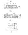
FIG. 1 is a cross-sectional view of an organic EL
display device according to one embodiment of the invention.
FIG. 2 is a cross-sectional view of an organic EL
display device according to another embodiment of the
invention.
FIG. 3 is a cross-sectional view showing the layer
arrangement of one exemplary organic EL multilayer structure
in the organic EL display device of the invention.
FIG. 4 illustrates a gastight working chamber for use
in the manufacture of the organic EL display device of the
invention.
FIG. 5 illustrates a system for manufacturing the
organic EL display device according to the invention.
FIG. 6 is a cross-sectional view taken along lines A-A
in FIG. 5, showing the working vacuum chamber serving as an
evaporation chamber.
FIG. 7 is a cross-sectional view taken along lines E-B
in FIG. 5, showing the working vacuum chamber serving as a
sputtering chamber.
FIG. 8 is a perspective view showing a receiving
platform in the working vacuum chamber relative to a robot
arm.
FIG. 9 is a cross-sectional view similar to FIG. 6,
showing another exemplary working vacuum chamber serving as
an evaporation chamber.
FIG. 10 is a cross-sectional view similar to FIG. 7,
showing another exemplary working vacuum chamber serving as
a sputtering chamber.
Device
Referring to FIG. 1, there is illustrated an organic EL
display device according to one embodiment of the invention.
The organic EL display device is illustrated in FIG. 1 as
comprising a substrate D1, an organic EL multilayer
structure D10 on the substrate D1, and a box-shaped shield
member D20 disposed on the substrate D1 and enclosing the
organic EL multilayer structure D10.
The shield member D20 is preferably formed of glass,
metals, ceramics, or low moisture permeable polymers. The
shield member D20 is a continuous member which is one piece
as a whole and does not have a filling port or other
opening. In the illustrated example, the box-shaped shield
member D20 consists of a rectangular top member D21 and a
side wall D22 extending perpendicularly from the entire
periphery of the top member D21. Since the organic EL
multilayer structure D10 usually has an overall height of
about 300 nm to about 500 nm, the side wall D22 is
preferably set to a height of about 1 µm to about 500 µm.
The lower end of the side wall D22 is closely secured to the
substrate D1 with an adhesive D30 to define a gastight space
D40 between the substrate D1 and the shield member D20. The
adhesive used herein is a UV-curing epoxy resin adhesive of
the cationic curing type. Since layer-forming materials of
the organic EL multilayer structure usually have a glass
transition temperature of at most about 140°C, typically
from about 80°C to about 100°C, the use of conventional
thermosetting adhesives having a curing temperature of about
140°C to about 180°C gives rise to the problem that upon
curing of the adhesive, the organic EL multilayer structure
can soften and deteriorate its characteristics. In
contrast, UV-curing adhesives do not give rise to the
problem that the organic EL multilayer structure can soften.
However, the currently available UV-curing adhesives yet
have the problem that since they are acrylic base adhesives,
acrylic monomers can volatilize upon curing of the adhesive,
which adversely affects the layer-forming materials of the
organic EL multilayer structure to deteriorate its
characteristics. Searching for the adhesive which
eliminates or minimizes this problem, we have found that a
UV-curing epoxy resin adhesive of the cationic curing type
is best suited.
It is noted that UV-curing/thermosetting combined type
epoxy resin adhesives are encompassed in commercially
available UV-curing epoxy resin adhesives. Since most of
these adhesives are obtained by the mixing or modification
of acrylic resins of the radical curing type with
thermosetting epoxy resins, they have not solved the acrylic
monomer volatilization problem of acrylic resins and the
curing temperature problem of thermosetting epoxy resins.
Then, the UV-curing/thermosetting combined type epoxy resin
adhesives are not desirable as the adhesive for use in the
manufacture of organic EL display devices of the invention.
The UV-curing epoxy resin adhesive of the cationic
curing type, as used herein, is an adhesive composition
comprising an epoxy resin as a base component and a Lewis
acid salt type curing agent as a main curing agent which
upon exposure to light containing UV radiation, releases a
Lewis acid catalyst through photolysis whereby the epoxy
resin polymerizes and cures through a reaction mechanism of
cationic polymerization type. The epoxy resins used as the
base component of the adhesive include epoxidized olefinic
resins, alicyclic epoxy resins, and novolak epoxy resins.
Examples of the curing agent include Lewis acid salts of
aromatic diazonium, Lewis acid salts of diallyl iodonium,
Lewis acid salts of triallyl sulfonium, and Lewis acid salts
of triallyl selenium.
The gastight space D40 is filled with an inert gas such
as helium, argon and nitrogen. The inert gas contained in
the space D40 should desirably have a water content of up to
100 ppm, more desirably up to 10 ppm, most desirably up to 1
ppm. The water content has no particular lower limit
although the lower limit is usually about 0.1 ppm.
Although the shield member of box shape is illustrated
in the above embodiment, the shield member may be a tabular
member D50 as shown in FIG. 2. In the embodiment of FIG. 2
wherein the plate-shaped shield member D50 is used, using a
suitable adhesive dispenser, the adhesive is previously
applied to the substrate D1 to form a desired pattern of
adhesive. The adhesive is cured to form a spacer D60 which
should have a height which is slightly greater than the
height of the organic EL multilayer structure D10. The
plate-shaped shield member D50 is then placed on the spacer
D60 and secured thereto with an adhesive D30, to thereby
define the gastight space D40. In this embodiment, the
space D40 is defined by the substrate D1, the shield member
D50, and the adhesive spacer D60, D30. Since the organic EL
multilayer structure D10 usually has an overall height of
about 300 nm to about 500 nm, the spacer D60 is preferably
set to a height of about 1 µm to about 500 µm. The gastight
space D40 is also filled with an inert gas having a low
water content as in the first embodiment.
In one preferred embodiment, fine particles having a
certain rigidity are dispersed in the adhesive D30 whereby
the layer formed by the adhesive D30 itself also serves for
the function of a spacer. That is, the layer formed by the
adhesive D30 itself also serves as the spacer D60. The fine
particles used herein preferably have a diameter of about 1
to 500 µm, especially about 5 to 100 µm. They are
preferably formed of polymers such as divinylbenzene,
benzoguanamine or styrene or inorganic materials such as
silica, glass fibers or glass beads.
Preferably the adhesive is loaded with about 0.1 to
30%, especially 1 to 10% by weight of fine particles based
on the total weight of the adhesive and particles. The
adhesive loaded with less than 0.1% of fine particles would
not achieve the full function as a spacer because the number
of fine particles dispersed per unit area is too small.
Loading of more than 30% of fine particles is undesirable
because fine particles tend to agglomerate so that the layer
of the loaded adhesive may occupy a thickness greater than
the diameter of discrete fine particles, application of the
loaded adhesive through a dispenser would become difficult
due to the increased viscosity, and sufficient bond strength
would not be achieved.
In either of the structural embodiments of the organic
EL display device, the adhesive for joining the shield
member to the substrate should preferably be spaced apart
from the organic EL multilayer structure. If the adhesive
is in contact with the organic EL multilayer structure, the
adhesive might penetrate between layers of the organic EL
multilayer structure, causing separation and hence,
deterioration.
Referring to FIG. 3, one exemplary layer arrangement of
the organic EL multilayer structure D10 in FIGS. 1 and 2 is
described.
The organic EL multilayer structure D10 includes a hole
injecting electrode D11, a hole injecting and transporting
layer D12, a light emitting layer D13, an electron injecting
and transporting layer D14, and an electron injecting
electrode D15 stacked on the substrate D1 in the described
order.
The layer arrangement of the organic EL multilayer
structure which can be used herein is not limited to the
illustrated one. Various other layer arrangements are
possible. For example, the light emitting layer and the
electron injecting and transporting layer may be mixed into
a single layer. Alternatively, the light emitting layer may
be mixed with the hole injecting and transporting layer if
necessary.
In the construction wherein light emission emanates on
the substrate side, the substrate is formed of a transparent
or translucent material such as glass, quartz or resins.
The substrate may be provided with a color filter film,
fluorescent material-containing color conversion film or
dielectric reflecting film for controlling the color of
light emission.
A transparent electrode is used as the hole injecting
electrode. The material and thickness of the hole injecting
electrode are preferably determined so that at least 80% of
the emitted light may be transmitted by the electrode. For
example, tin-doped indium oxide (ITO), zinc-doped indium
oxide (IZO), SnO2 and doped polypyrrole are useful for the
hole injecting electrode. The thickness of the hole
injecting electrode is typically about 10 to about 500 nm.
For effective electron injection, the electron
injecting electrode is preferably formed of materials having
a low work function, for example, metal elements such as K,
Li, Na, Mg, La, Ce, Ca, Sr, Ba, Al, Ag, In, Sn, Zn, and Zr
and binary and ternary alloys containing two or three of
them for improving stability. Preferred alloys are Ag-Mg
(Ag: 1 to 20 at%), In-Mg (Mg: 50 to 80 at%), and Al-Ca (Ca:
5 to 20 at%). In forming the electron injecting electrode,
any of these metals and alloys is used as the target.
The electron injection electrode is usually formed as a
thin film having a sufficient thickness to ensure electron
injection, typically at least 50 nm, preferably at least 100
nm. The upper limit is not critical although the film
thickness is usually about 100 to 500 nm.
Next, the organic material layers included in the
organic EL multilayer structure according to the invention
are described.
The light emitting layer has the functions of injecting
holes and electrons, transporting them, and recombining
holes and electrons to create excitons. It is preferred
that relatively electronically neutral compounds be used in
the light emitting layer.
The hole transporting layer, which is also referred to
as a hole injecting and transporting layer, has the
functions of facilitating injection of holes from the hole
injecting electrode, transporting holes, and obstructing
electron transportation.
The electron injecting and transporting layer has the
functions of facilitating injection of electrons from the
electron injecting electrode, transporting electrons, and
obstructing hole transportation. It is desirable that this
electron injecting and transporting layer is provided when
the compound used in the light emitting layer has a
relatively low electron injecting and transporting function.
The hole and electron injecting and transporting layers
are effective for increasing the number of holes and
electrons injected into the light emitting layer and
confining holes and electrons therein for optimizing the
recombination region to improve light emission efficiency.
Each of the hole and electron injecting and transporting
layers may be constructed by separately providing a layer
having an injecting function and a layer having a
transporting function.
The thickness of the light emitting layer, the hole
injecting and transporting layer, and the electron injecting
and transporting layer is not critical and varies with a
particular formation technique although it is usually
preferred to range from about 5 nm to about 100 nm,
especially about 10 nm to about 100 nm.
The thickness of the hole injecting and transporting
layer and the electron injecting and transporting layer is
equal to or ranges from about 1/10 times to about 10 times
the thickness of the light emitting layer although it
depends on the design of a recombination/light emitting
region. When the electron or hole injecting and
transporting layer is divided into an injecting layer and a
transporting layer, preferably the injecting layer is at
least 1 nm thick and the transporting layer is at least 1
nm, especially at least 20 nm thick. The upper limit of
thickness is usually about 500 nm, especially about 100 nm
for the injecting layer and about 500 nm, especially about
100 nm for the transporting layer. The same film thickness
applies when two injecting/transporting layers are provided.
By controlling the layer thickness while taking into
account the carrier mobility and carrier density (dependent
on ionization potential and electron affinity) of the light
emitting layer, the hole injecting and transporting layer,
and the electron injecting and transporting layer to be
combined, the free design of a recombination/light emitting
region, the design of emission color, the control of the
luminance and spectrum of light emission by the interference
of both the electrodes, and the control of the spatial
distribution of light emission become possible.
The light emitting layer contains a fluorescent
material that is a compound having a light emitting
capability. The fluorescent material may be selected from
metal complex dyes such as tris(8-quinolinolato)aluminum as
disclosed in JP-A 264692/1988, for example. Additionally,
quinacridone, coumarin, rubrene, and styryl dyes,
tetraphenylbutadiene, anthracene, perylene, coronene, and
12-phthaloperinone derivatives may be used alone or in
admixture with the metal complex dye. In the embodiment
wherein the light emitting layer also serves as an electron
injecting and transporting layer, the use of tris(8-quinolinolato)aluminum
is preferred. These fluorescent
materials can be evaporated or otherwise deposited.
For the electron injecting and transporting layer,
there may be used organic metal complexes such as tris(8-quinolinolato)aluminum
(Alq3), oxadiazole derivatives,
perylene derivatives, pyridine derivatives, pyrimidine
derivatives, quinoline derivatives, quinoxaline derivatives,
diphenylquinone derivatives, and nitro-substituted fluorene
derivatives. The electron injecting and transporting layer
can also serve as a light emitting layer as previously
mentioned. In this case, use of tris(8-quinolinolato)-aluminum
etc. is preferred. Like the light emitting layer,
the electron injecting and transporting layer may be formed
by evaporation or the like.
Where the electron injecting and transporting layer is
formed as comprising an electron injecting layer and an
electron transporting layer, two or more compounds are
selected in a proper combination from the compounds commonly
used in electron injecting and transporting layers. In this
regard, it is preferred to laminate layers in such an order
that a layer of a compound having a greater electron
affinity may be disposed adjacent the electron injecting
electrode. This order of lamination also applies where a
plurality of electron injecting and transporting layers are
provided.
For the hole injecting and transporting layer, there
may be used various organic compounds as described in JP-A
295695/1988, 191694/1990, 000792/1991, 234681/1993,
239455/1993, 299174/1993, 126225/1995, 126226/1995, and
100172/1996 and EP 0650955A1. Examples are tetraarylene-benzidine
compounds (triaryldiamine or triphenyldiamine
(TPD)), aromatic tertiary amines, hydrazone derivatives,
carbazole derivatives, triazole derivatives, imidazole
derivatives, oxadiazole derivatives having an amino group,
and polythiophenes. These compounds may be used in a
combination of two or more and for the combined use, they
may be stacked as separate layers or mixed.
Where the hole injecting and transporting layer is
formed as comprising a hole injecting layer and a hole
transporting layer, two or more compounds are selected in a
proper combination from the compounds commonly used in hole
injecting and transporting layers. In this regard, it is
preferred to laminate layers in such an order that a layer
of a compound having a lower ionization potential may be
disposed adjacent the hole injecting electrode (ITO etc.).
It is also preferred to use a compound having good thin film
forming ability at the anode surface. The order of
lamination also applies where a plurality of hole injecting
and transporting layers are provided. Such an order of
lamination is effective for lowering drive voltage and
preventing the occurrence of current leakage and the
appearance and growth of dark spots. Since evaporation is
utilized in the manufacture of devices, films as thin as
about 1 to 10 nm can be formed uniform and pinhole-free,
which restrains any change in color tone of light emission
and a drop of efficiency by re-absorption even if a compound
having a low ionization potential and absorption in the
visible range is used in the hole injecting layer. Like the
light emitting layer and the like, the hole injecting and
transporting layer can be formed by evaporating the above-mentioned
compounds.
The organic EL multilayer structure of the invention
may be prepared in a conventional way. For example, the
light emitting layer and other organic material layers may
be formed by vacuum evaporation, and the hole injecting
electrode and the electron injecting electrode may be formed
by evaporation or sputtering. If necessary, these layers
can be patterned, for example, by mask evaporation or film
formation followed by etching whereby a desired light
emitting pattern is accomplished. If the substrate bears
thin film transistors (TFT), the respective layers may be
formed in accordance with the pattern of TFT to accomplish a
display or drive pattern without further treatment.
Finally, a protective layer may be formed over the structure
using inorganic materials such as SiOx and organic materials
such as Teflon®.
The organic EL element of the invention is generally of
the DC drive type while it can be of the AC or pulse drive
type. The drive voltage should preferably be low in order
to improve the reliability of the device. The applied
voltage is generally about 5 to 20 volts.
Method
Next, the method for manufacturing the organic EL
display device is described. The method is characterized by
the step of attaching the shield member D20 to the substrate
D1 having the organic EL multilayer structure D10 borne
thereon, that is, sealingly enclosing the organic EL
multilayer structure D10 in the shield member D20, which is
first described below.
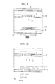
Before the start of the enclosing step, a gastight
working chamber 100 is furnished as shown in FIG. 4. The
gastight working chamber 100 includes a main working chamber
110 and optionally, a gastight fore-chamber 120 and a
gastight aft-chamber 130.
Selectively openable and closable gastight shutters 121
and 131 are disposed between the main working chamber 110
and fore- and aft- chambers 120 and 130 for maintaining the
main working chamber 110 gastight. A third gastight shutter
122 is disposed at the inlet of the fore-chamber 120 which
is otherwise open to the ambient air and through which the
components of the organic EL display device are carried in.
The third gastight shutter 122 cooperates with the first
gastight shutter 121 to maintain the fore-chamber 120
gastight. A fourth gastight shutter 132 is disposed at the
outlet of the aft-chamber 130 which is otherwise open to the
ambient air and through which the completed organic EL
display device are carried out. The fourth gastight shutter
132 cooperates with the second gastight shutter 131 to
maintain the aft-chamber 130 gastight.
The main working chamber 110, fore-chamber 120 and aft-chamber
130 are connected to an inert gas source 150 through
first, second and third valves 140, 141 and 142. The inert
gas source 150 reserves the same inert gas as contained in
the space D40 of the organic EL display device (FIGS. 1 and
2) and is capable of feeding the inert gas to the main
working chamber 110, fore-chamber 120 and aft-chamber 130.
The main working chamber 110, fore-chamber 120 and aft-chamber
130 are also connected to first, second and third
vacuum pumps 160, 161 and 162, respectively, for evacuating
the respective chambers. It is acceptable to connect the
first vacuum pump 160 connected to the main working chamber
110 to the second and third vacuum pumps 161 and 162 so that
all the chambers may initially be evacuated by means of the
first vacuum pump 160. To this end, the first vacuum pump
160 should preferably have a greater capacity.
The fore-chamber 120 is preferably provided with a
heater 123 for heating the fore-chamber 120 for causing any
residual water in the components of the organic EL display
device (that is, the organic EL multilayer structure D10 on
the substrate D1 and the shield member D20) to evaporate
off. Typically, the interior of the fore-chamber 120 is
heated at about 60 to 70°C for about 1 to 5 hours under a
vacuum of about 1 to 10-1 Pa. The heater 123 is preferably
an electric heater. While a thermometer in the form of a CA
(chromel-alumel) thermocouple (not shown) is provided within
the fore-chamber 120 for measuring the temperature thereof,
the temperature within the fore-chamber 120 is program
controlled within the range from room temperature to about
200°C by the proportional integral and derivative (PID)
control process. To achieve satisfactory temperature
control in a vacuum atmosphere, an electric heater having a
power of 1 kW or more is preferably used.
It is noted that the gastight fore-chamber 120 is
preferably disposed contiguous to a film forming section
where layers are deposited to form the organic EL multilayer
structure (as will be illustrated later in FIG. 5).
On the other hand, the gastight aft-chamber 130 is
provided with an adhesive curing means 133 for causing the
adhesive to cure for joining the substrate D1 having the
organic EL multilayer structure D10 borne thereon to the
shield member D20. The adhesive curing means 133 is a UV
radiation emitting device, which emits UV radiation at an
illuminance of 50 to 1,000 mW/cm2 so that the adhesive may be
fully cured within an appropriate irradiation time, for
example, of about 5 to 100 seconds.
It is now described how to manufacture the organic EL
display device using the gastight working chamber 100.
Since the procedures for forming the layers or films of the
organic EL multilayer structure D10 on the substrate D1 may
be the same as in the prior art, the description about these
procedures is omitted herein. The following description is
based on the assumption that the organic EL multilayer
structure D10 has already been formed on the substrate D1.
First, the main working chamber 110 and the aft-chamber
130 of the gastight working chamber 100 are evacuated or
degassed and instead, the inert gas is introduced into these
chambers. The evacuation and inert gas injection are
repeated several times until an inert gas atmosphere having
a purity of 90 to 99.9%, especially 99.0 to 99.9% and a
water content of up to 100 ppm, preferably up to 10 ppm,
especially up to 1 ppm is established in the chambers. The
lower the water content, the better become the results. In
the state of the art, the minimum ultimate water content is
about 0.1 ppm. After the aim water content is reached for
the inert gas atmosphere, an inert gas having a lower water
content than that inert gas atmosphere is circulated through
the chambers to maintain the water content at or below the
once reached level.
Next, the third shutter 122 is opened, and a plurality
of organic EL multilayer structures D10 and shield members
D20 or D50 are carried into the fore-chamber 120, whereupon
the third shutter 122 is closed again. At this point, the
fore-chamber 120 is evacuated, preferably to a vacuum of
about 1 to 10-1 Pa.
In the fore-chamber 120, with the vacuum of about 1 to
10-1 Pa kept, the heater 123 is energized to heat the organic
EL multilayer structures D10 and the shield members D20 or
D50 for removing residual water therefrom.
After the residual water is removed, the first shutter
121 is opened, and the organic EL multilayer structures and
the shield members are carried into the main working chamber
110 where the adhesive is applied to joint portions of the
substrates of the organic EL multilayer structures and/or
the shield members. Then, the shield members are joined to
the substrates of the organic EL multilayer structures at
their joint portions into assemblies. It is preferred that
the organic EL multilayer structures and the shield members,
prior to the application of the adhesive, are left to stand
for a certain time in the main working chamber, that is, the
inert gas atmosphere until the residual water contents in
the structures and the shield members reach equilibrium with
the water content in the inert gas atmosphere, and
thereafter, the adhesive is applied to the joint portions.
Thereafter, the second shutter 131 is opened, and the
finished assemblies are carried to the aft-chamber 130 where
the adhesive curing means 133 is energized to irradiate UV
radiation to the adhesive for curing, thereby completing the
organic EL display devices shown in FIG. 1 or 2.
Finally, the fourth shutter 132 is opened whereupon the
completed organic EL display devices are taken out.
In this way, organic EL display devices having the
gastight space D40 filled with the inert gas can be
manufactured without a need for a filling port.
System
Next, one preferred embodiment of the system for
manufacturing the organic EL display devices according to
the invention is described.
Referring to FIG. 5, the system includes a film forming
section LP where layers of organic EL multilayer structures
are formed and an assembly section MP where shield members
are joined to the organic EL multilayer structures. The
film forming section LP and the assembly section MP are
connected in a gastight manner. The assembly section MP is
the same as illustrated in FIG. 4.
The film forming section LP includes a hollow cylinder
shaped vacuum vessel 1, a robot 2, a holder 3, an organic EL
wafer 4, a substrate entrance 10, working vacuum chambers 11
to 15, an organic EL multilayer structure transition portion
16, and gate valves 20.
The robot 2 is installed within the vacuum vessel 1.
The working vacuum chambers 11 to 15 are disposed around the
periphery of the vacuum vessel 1 in a cluster fashion and
communicated thereto through the gate valves 20. The vacuum
vessel 1 is provided with the sealingly closable substrate
entrance 10 which receives the organic EL wafer 4 having a
transparent electrode D11 formed on a glass substrate D1.
The wafer 4 is caught by the robot 2, pulled into the vacuum
vessel 1 through the substrate entrance 10, and successively
moved into and out of the working vacuum chambers 11 to 15
in this order or in any desired order whereby a hole
injecting and transporting layer D12, a light emitting layer
D13, an electron injecting and transporting layer D14, an
electron injecting electrode D15, and an aluminum protective
or sealing layer (not shown) are successively formed on the
wafer 4 to produce the organic EL multilayer structure.
The robot 2 is constructed such that the organic EL
wafer 4 may be successively moved into and out of the
working vacuum chambers 11 to 15. To this end, the robot 2
has three arms 2-1, 2-2 and 2-3, for example. These arms 2-1,
2-2 and 2-3 are interlocked such that the holder 3 formed
at the tip of the third arm 2-3 may be movable and rotatable
in all 360° directions in vertical and horizontal planes.
The holder 3 holds a holding plate 5 having the organic
EL wafer 4 rested thereon. The holder 3 is bifurcated into
fingers 3-1 and 3-2 adapted to be inserted into counter
slots 6-1 and 6-2 in a receiving platform 6 to be described
later in FIG. 8.
The first working vacuum chamber 11 is, for example, a
chamber in which the step of forming the hole injecting and
transporting layer D12 is performed by evaporation. FIG. 6
is a cross section of the first chamber 11 taken along lines
A-A in FIG. 5. As shown in the cross-sectional view of FIG.
6, the first working vacuum chamber 11 includes the
receiving platform 6, a heater 7, and an evaporation source
17.
The receiving platform 6 adapted to receive the holding
plate 5 having the organic wafer 4 rested thereon is formed
with the slots 6-1 and 6-2 as shown in FIG. 8. In the state
shown in FIG. 8, the robot 2 is operated to move the holder
3 to the right whereby the fingers 3-1 and 3-2 are inserted
into the slots 6-1 and 6-2 of the receiving platform 6.
During this movement, the upper surface of the fingers 3-1
and 3-2 is held slightly higher than the upper surface of
the receiving platform 6, and hence, the holding plate 5 is
moved to above the receiving platform. Just when the
holding plate 5 reaches the predetermined position, the
holder 3 is moved down whereupon the holding plate 5 is left
on the receiving platform 6 at the predetermined position.
In this state, the gate valve 20 is closed and
electricity is conducted through the heater 7 to heat the
evaporation source 17 whereby the source material is
evaporated onto the organic EL wafer 4. After the
completion of evaporation, the gate valve 20 is opened again
and the robot 2 is operated so as to move the holder 3 to
insert the fingers 3-1 and 3-2 into the slots 6-1 and 6-2
while the upper surface of the fingers 3-1 and 3-2 is held
lower than the upper surface of the receiving platform 6.
Just when the holder 3 reaches the predetermined position,
it is slightly moved up whereby the evaporated organic EL
wafer 4 is rested on the holder 3 again. The robot 2 is
operated so that the wafer 4 is moved out of the first
working vacuum chamber 11. Thereafter, the wafer 4 is
similarly moved into the second working vacuum chamber 12
and placed on the receiving platform 6 in the second chamber
12. In this way, film formation is successively performed
on the wafer in a series of working vacuum chambers. It is
noted that when a mask 9 is furnished as shown in FIG. 8,
mask evaporation is possible by positioning the mask 9 above
the organic EL wafer 4.
For example, the second working vacuum chamber 12 is to
evaporate the light emitting layer D13, the third working
vacuum chamber 13 is to evaporate the electron injecting and
transporting layer D14, and the fourth working vacuum
chamber 14 is to evaporate the electron injecting electrode
D15. These chambers are of the same construction as the
first working vacuum chamber 11 shown in FIG. 6.
The fifth working vacuum chamber 15 is, for example, a
chamber in which the step of forming an aluminum layer is
performed by sputtering. FIG. 7 is a cross section of the
fifth chamber 15 taken along lines B-B in FIG. 5. As shown
in the cross-sectional view of FIG. 7, the sputtering vacuum
chamber 15 also includes a receiving platform 6 as in the
evaporating vacuum chambers, an electrode 18 disposed above
the receiving platform 6, and a target 19 disposed close to
and below the electrode 18. An RF source 8 applies an RF
voltage across the electrode 18 to generate in the chamber
an RF discharge by which the target 19 is sputtered, while
argon gas is introduced into the chamber. The aluminum
layer is formed on the organic EL wafer 4 rested on the
receiving platform 6.
The working vacuum chambers 11 to 14 and the working
vacuum chamber 15 are disposed around the vacuum vessel 1 in
a cluster arrangement.
The operation of the film forming section LP is
described below. First, the organic EL wafer 4 having the
transparent electrode Dll formed on the glass substrate Dl
is rested on the holding plate 5, which is moved into the
vacuum vessel 1 through the window of the substrate entrance
10 and rested on the holder 3 of the robot 2. The gate
valves 20 associated with the respective working vacuum
chambers 11 to 15 are opened and the vacuum vessel 1 is
evacuated by means of a vacuum pump (not shown).
When the vacuum vessel 1 is evacuated to the
predetermined pressure, the holder 3 of the robot 2 is moved
into the first chamber 11, the holding plate 5 having the
organic EL wafer 4 rested thereon is placed on the receiving
platform 6 as mentioned above, and the gate valve 20 is then
closed. The heater 7 is energized to heat the evaporation
source 17 to evaporate the hole injecting and transporting
material, thereby forming the hole injecting and
transporting layer D12.
After the hole injecting and transporting layer D12 is
formed in this way, the gate valve 20 associated with the
first chamber 11 is opened, and the robot 2 is operated such
that the holding plate 5 on which the organic EL wafer 4
having the hole injecting and transporting layer D12 formed
thereon rests is held by the holder 3 of the robot, moved
out of the first chamber 11, moved into the second chamber
12, and placed on the receiving platform 6 in the second
chamber. The gate valve 20 associated with the second
chamber 12 is closed. The heater 7 is energized to heat the
evaporation source 17 to evaporate the light emitting
material, thereby forming the light emitting layer D13.
After the light emitting layer D13 is formed, the gate
valve 20 associated with the second chamber 12 is opened,
and the robot 2 is operated such that the holding plate 5 on
which the organic EL wafer 4 having the light emitting layer
D13 formed thereon rests is held by the holder 3 of the
robot, moved out of the second chamber 12, moved into the
third chamber 13, and placed on the receiving platform 6 in
the third chamber. The gate valve 20 associated with the
third chamber 13 is closed. The heater 7 is energized to
heat the evaporation source 17 to evaporate the electron
injecting and transporting material, thereby forming the
electron injecting and transporting layer D14.
After the electron injecting and transporting layer D14
is formed in this way, the gate valve 20 associated with the
third chamber 13 is opened, and the robot 2 is operated such
that the holding plate 5 on which the organic EL wafer 4
having the electron injecting and transporting layer D14
formed thereon rests is held by the holder 3 of the robot,
moved out of the third chamber 11, moved into the fourth
chamber 14, and placed on the receiving platform 6 in the
fourth chamber. The gate valve 20 associated with the
fourth chamber 14 is closed. The heater 7 is energized to
heat the evaporation source 17 to evaporate the electron
injecting material, thereby forming the electron injecting
electrode D15.
After the electron injecting electrode D15 is formed,
the gate valve 20 associated with the fourth chamber 14 is
opened, and the robot 2 is operated such that the holding
plate 5 on which the organic EL wafer 4 having the electron
injecting electrode D15 formed thereon rests is held by the
holder 3 of the robot, moved out of the fourth chamber 14,
moved into the fifth chamber 15, and placed on the receiving
platform 6 in the fifth chamber. The gate valve 20
associated with the fifth chamber 15 is closed. An RF
voltage is applied across the electrode 18 from the RF
source 8 to generate an RF discharge, thereby sputtering the
target 19 to form an aluminum layer on the organic EL wafer
4.
After the aluminum layer is formed in this way, the
gate valve 20 associated with the fifth chamber 15 is
opened, and the robot 2 is operated such that the holding
plate 5 on which the organic EL multilayer structure rests
is carried to the transition portion 16 which is kept
vacuum.
Although the receiving platform 6 is positioned on the
bottom of the working vacuum chamber in the illustrated
embodiment, the position of the receiving platform 6 is not
limited thereto. Another working vacuum chamber 11' for
evaporation is shown in FIG. 9 wherein the receiving
platform 6 is positioned near the top of the chamber and the
heater 7 and the evaporation source 17 are positioned near
the bottom of the chamber. In this embodiment, a plurality
of claws 21 are provided for holding the wafer 4 at its
edge. Blocks 22 shown by broken lines designate the areas
into which the fingers 3-1 and 3-2 of the holder 3 are
inserted.
Similarly in a working vacuum chamber 15' for
sputtering as shown in FIG. 10, the electrode 18 and the
target 19 may be positioned near the bottom and the
receiving platform 6 positioned near the top of the chamber.
In these modified embodiments, as a matter of course,
the organic EL wafer 4 is faced toward the evaporation
source 17 or target 19. The receiving platform 6 is
provided with an opening so that when the holding plate 5 is
rested on the platform 6, the organic EL wafer 4 is
positioned in the opening.
Although the arrangement of the working vacuum chambers
is counterclockwise in accordance with the order of steps in
the embodiment illustrated in FIG. 5, the arrangement of the
working vacuum chambers is not limited to the order of steps
and may be arbitrary insofar as the robot 2 can be operated
to drive its holder 3 and hence, the organic EL wafer in
accordance with the order of steps. Of course, the order of
steps may also be clockwise as viewed in FIG. 5.
The number of working vacuum chambers is not limited to
the embodiment illustrated in FIG. 5. The number of
chambers may be increased or decreased as the number of
steps is increased or decreased in accordance with an
appropriate number of layers.
Although the cluster type arrangement of the vacuum
vessel surrounded by a series of working vacuum chambers is
described in the above embodiment, an in-line arrangement
wherein working vacuum chambers are arranged in a straight
line may also be used.
The assembling section MP is of substantially the same
construction as the gastight working chamber shown in FIG.
4. As shown in FIG. 5, the main working chamber 110 is
tightly connected to the organic EL multilayer structure
transition portion 16 and optionally, to the gastight aft-chamber
130. Since the transition portion 16 of the
assembling section MP corresponds to the gastight fore-chamber
120 in FIG. 4, this is referred to as the fore-chamber
120, hereinafter. The fore-chamber 120 on an
opposite side to the main working chamber 110 is provided
with an inlet for carrying components of organic EL display
devices into the fore-chamber 120 where a third gastight
shutter 122 (or gate valve 20) is provided. The fore-chamber
120 is contiguous to the film forming section LP for
the manufacture of organic EL multilayer structures.
The remaining components of the assembling section MP
are the same as in FIG. 4. Like parts are designated by the
same numerals and their description is omitted.
The method for manufacturing organic EL display devices
using the above-mentioned system is now described. The
manufacturing method is substantially the same as the method
described in conjunction with FIG. 4. Only the description
of different points is supplemented and the description of
common steps is omitted.
The gastight aft-chamber 130 is provided with an
adhesive curing means 133 for curing the adhesive for
joining shield members D20 to substrates D1 having organic
EL multilayer structures D10 borne thereon. The adhesive
curing means 133 may be either a heater when the adhesive
used is of the thermosetting type or a UV source when the
adhesive used is of the UV curing type. As previously
mentioned, if the organic EL multilayer structures are
heated above the glass transition temperatures (about 80 to
100°C) of the respective organic materials, the structures
are deteriorated due to the softening of the organic
materials. It is thus preferred to use UV curing type
adhesives and hence, to use a UV source as the adhesive
curing means 133. To fully cure the adhesive within an
appropriate irradiating time, for example, of several
seconds to several ten minutes, a UV source capable of
providing an illuminance of 50 to 1,000 mW/cm2 is used.
The main working chamber 110 and aft-chamber 130 of the
gastight working chamber 100 are evacuated and filled with
an inert gas so that an inert gas atmosphere having a water
content of at most 100 ppm may be established in the main
working chamber 110 and aft-chamber 130. To establish an
inert gas atmosphere having a water content of at most 100
ppm in the main working chamber 110 and aft-chamber 130, an
inert gas circulating loop may be provided which passes the
main working chamber 110 and aft-chamber 130 and includes a
means for drying the inert gas. Then the moisture in the
respective chambers can be gradually removed while
circulating the inert gas through the loop. The respective
chambers are given an inert gas atmosphere meeting the above
requirement.
In the system of FIG. 5, it is desired that shield
members are previously delivered to the predetermined
position within the vacuum vessel 1 by means of the robot 2
approximately at the same time as are the organic EL wafers.
Alternatively, an additional chamber receiving shield
members is connected to the fore-chamber 120 or main working
chamber 110 in a gastight manner so that shield members may
be delivered from the additional chamber to the fore-chamber
120 or main chamber 110 by means of a robot.
After the fore-chamber 120 is filled with the same
inert gas as in the main chamber 110, the first shutter 121
is opened, and organic EL multilayer structures and shield
members are carried into the main working chamber 110 where
the adhesive is applied to joint portions of substrates of
the organic EL multilayer structures and the shield members.
The shield members are joined to the substrates of the
organic EL multilayer structures to form assemblies.
Thereafter, the second shutter 131 is opened, and the
assemblies are carried into the gastight aft-chamber 130
where the adhesive curing means 133 is energized to cure the
adhesive, completing organic EL display devices of the
structure shown in FIG. 1 or 2.
Finally, the fourth shutter 132 is opened and the
completed organic EL display devices are taken out.
In this way, organic EL display devices in which the
gastight space D40 is filled with the inert gas can be
manufactured without a need for a filling port.
Although the multilayer structure layer forming section
and the shield member assembling section are tightly coupled
in the system illustrated in FIG. 5, they need not
necessarily be coupled in a gastight manner. When these
sections are separate, it is desired to employ a carrier box
combined with a conveyor. The carrier box is formed of a
metal material such as aluminum or stainless steel or a
polymeric material having low moisture permeability and low
moisture absorption, that is, formed as a gastight box. The
interior atmosphere of the carrier box is vacuum or an inert
gas having a water content of at most 100 ppm. The inert
gas is typically nitrogen or argon gas. The interior
atmosphere is preferably coincident with the atmosphere of
the shield member assembling section. The carrier box in
which organic EL multilayer structures are accommodated is
moved from the layer forming section to the assembling
section. This movement may be done by a chain conveyor or a
carriage. The transfer of organic EL multilayer structures
from the film forming section to the carrier box and from
the carrier box to the assembling section is also performed
in a vacuum chamber or an inert gas atmosphere so that the
organic EL multilayer structures may never be exposed to the
ambient air. The use of the carrier box serving as a
gastight box is encompassed in the system in which the
multilayer structure layer forming section and the shield
member assembling section are coupled in a gastight manner.
EXAMPLE
Examples of the present invention are given below by
way of illustration.
Example 1
On a glass substrate of 1.1 mm thick, a transparent
electrode was formed to a thickness of 200 nm by sputtering
ITO in a predetermined pattern. The substrate was subjected
to ultrasonic washing with neutral detergent, acetone, and
ethanol, pulled up from boiling ethanol, and dried. After
the surface of the transparent electrode was cleaned with
UV/ozone, the substrate was secured by a holder in a vacuum
evaporation chamber, which was evacuated to a vacuum of 1x10⁻⁴
Pa or lower.
With the vacuum kept, 4,4',4"-tris(3-methylphenyl-phenylamino)phenylamine
(MTDATA) was evaporated at a
deposition rate of 0.2 nm/sec. to a thickness of 40 nm,
forming a hole injecting layer. With the vacuum kept,
N,N,N',N'-tetrakis(3-biphenyl)-4,4'-diamino-1,1'-biphenyl
(TPD) was evaporated at a deposition rate of 0.2 nm/sec. to
a thickness of 35 nm, forming a hole transporting layer.
With the vacuum kept, tris(8-quinolinolato)aluminum
(Alq3) was evaporated at a deposition rate of 0.2 nm/sec. to
a thickness of 50 nm, forming an electron injecting and
transporting/light emitting layer.
The substrate having these layers formed thereon was
then carried from the vacuum evaporation chamber to a
sputtering chamber where using an Ag-Mg alloy (Mg 5 at%) as
the target, an electron injecting electrode was formed by a
DC sputtering technique at a deposition rate of 15 nm/min.
to a thickness of 200 nm. Argon was used as the sputtering
gas under a pressure of 0.5 Pa. The input power was 500
watts and the grid voltage was 6 volts. The thus obtained
electron injecting electrode thin film was observed for
surface smoothness under a scanning electron microscope,
finding a value of 10 nm ±20%.
Finally, aluminum was sputtered to a thickness of 200
nm as a protective and wiring layer, obtaining an organic EL
multilayer structure.
The gastight working chamber 100 shown in FIG. 4 was
conditioned as follows. The main working chamber 110 and
aft-chamber 130 of the gastight working chamber 100 were
evacuated and then filled with argon gas as the inert gas.
The evacuation and inert gas injection steps were repeated
three times. The chambers were finally filled with the
inert gas having a purity of 99.9% and a water content of 10
ppm.
Next, the third shutter 122 was opened, and a plurality
of organic EL multilayer structures D10 and shield members
D20 were carried into the fore-chamber 120. The third
shutter was then closed. In this state, the fore-chamber
120 was evacuated until a vacuum of 1x10⁻¹ Pa was established
in the chamber. The shield members were glass plates of 26
mm x 17 mm x 1.1 mm (thick) whose one surface had been
recessed to a depth of 0.5 mm to define a recess for
receiving the organic EL multilayer structure therein.
Thereafter, the first shutter 121 was opened, the
organic EL multilayer structures D10 and shield members D20
were carried into the main working chamber 110. An adhesive
was applied to joint portions of the substrates of the
organic EL multilayer structures and/or the shield members.
The adhesive used herein was a UV-curing epoxy resin
adhesive of the cationic curing type 30Y184G (Three Bond
K.K.). Then the substrates of the organic EL multilayer
structures and the shield members were joined at their joint
portions to form assemblies.
Thereafter, the second shutter 131 was opened, and the
assemblies were carried into the aft-chamber 130 where the
curing means 133 was energized to irradiate UV radiation to
the adhesive for curing. The UV illuminance was 100 mW/cm2
and the irradiating time was 60 seconds. In this way,
organic EL display devices of the structure shown in FIG. 1
were completed.
Finally, the fourth shutter 132 was opened, and the
completed organic EL display devices were taken out.
Example 2
Organic EL display devices were fabricated as in
Example 1 except that in the gastight fore-chamber 120, the
heater 123 was energized from the start of evacuation,
whereby a plurality of organic EL multilayer structures D10
and shield members D20 were heated in vacuum (at 60°C for 3
hours) for removing residual water.
Example 3
Organic EL display devices were fabricated as in
Example 1 except that the adhesive was cured in air.
Comparative Example 1
An organic EL display device of the structure shown in
FIG. 1 was fabricated. A shield member was of the same size
as in Example 1, but formed with a filling port. In air,
the shield member was adhesively joined to the substrate of
organic EL multilayer structure (which were the same as in
Example 1), and the adhesive was cured to form an assembly.
The gastight space defined in the assembly was evacuated and
filled with an inert gas (which was the same as in Example
1) through the filling port. The evacuation and inert gas
filling steps were repeated three times. The filling port
was blocked with the adhesive. The adhesive used was the
same as in Example 1.
Comparative Example 2
An organic EL display device was fabricated as in
Example 1 except that a UV curing acrylic resin adhesive of
the radical curing type TB-3050 (Three Bond K.K.) was used
instead of the adhesive used in Example 1.
The organic EL display devices fabricated in Examples 1
to 3 and Comparative Examples 1 to 2 were examined as
follows. With a DC voltage applied, the devices were
continuously driven in air at a constant current density of
10 mA/cm2. They all emitted green light having an emission
maximum wavelength λmax of 520 nm. The initial luminance
and the quarter-life of luminance (the life of a device when
its luminance lowers to a quarter of the initial luminance)
were measured. The devices were also observed for dark
spots. With respect to the formation of dark spots, the
devices were rated "Excellent" when dark spots having a
diameter of more than 100 µm did not generate after 3,000
hours of operation, "Good" when dark spots having a diameter
of more than 100 µm did not generate after 2,000 hours of
operation, "Fair" when dark spots having a diameter of more
than 100 µm did not generate after 1,000 hours of operation,
and "Poor" when dark spots having a diameter of more than
100 µm generated after 100 hours of operation.
The results are shown in Table 1.
| | Applied voltage | Initial luminance | Quarter-life of luminance | Dark spots |
| E1 | 8.1 V | 500 cd/m2 | >3000 hr. | Excel |
| E2 | 8.0 V | 490 cd/m2 | >3000 hr. | Excel |
| E3 | 7.9 V | 480 cd/m2 | >3000 hr. | Good |
| CE1 | 7.9 V | 490 cd/m2 | 500 hr. | Poor |
| CE2 | 8.1 V | 490 cd/m2 | 500 hr. | Poor |
The manufacturing system shown in FIG. 5 was used.
The gastight working chamber MP (or 100 in FIG. 4) was
conditioned as follows. The main working chamber 110 and
aft-chamber 130 of the gastight working chamber 100 were
evacuated and then filled with argon gas as the inert gas.
The evacuation and inert gas injection steps were repeated
three times. The chambers were finally filled with the
inert gas having a purity of 99.9% and a water content of 10
ppm.
Next, the third shutter 122 was opened, and a plurality
of organic EL multilayer structures D10 and shield members
D20, both prepared as in Examples 1 to 3, were carried into
the fore-chamber 120. The third shutter was then closed.
After the fore-chamber 120 was filled with argon gas,
the organic EL multilayer structures D10 and shield members
D20 were carried into the main working chamber 110. An
adhesive was applied to joint portions of the substrates of
the organic EL multilayer structures and/or the shield
members. The adhesive used herein was a UV-curing epoxy
resin adhesive of the cationic curing type 30Y184G (Three
Bond K.K.). Then the substrates of the organic EL
multilayer structures and the shield members were joined at
their joint portions to form assemblies.
Thereafter, the second shutter 131 was opened, and the
assemblies were carried into the aft-chamber 130 where the
curing means 133 was energized to irradiate UV radiation to
the adhesive for curing. The UV luminance was 100 mW/cm2 and
the irradiating time was 60 seconds. In this way, organic
EL display devices of the structure shown in FIG. 1 were
completed.
Finally, the fourth shutter 132 was opened, and the
completed organic EL display devices were taken out.
According to the present invention, organic EL display
devices having a long lifetime can be manufactured through a
smaller number of steps in a simple manner.
The invention has been described in detail with
particular reference to preferred embodiments thereof, but
it will be understood that variations and modifications can
be effected within the spirit and scope of the invention.