JP3969698B2 - Method for manufacturing light emitting device - Google Patents
Method for manufacturing light emitting device Download PDFInfo
- Publication number
- JP3969698B2 JP3969698B2 JP2001151572A JP2001151572A JP3969698B2 JP 3969698 B2 JP3969698 B2 JP 3969698B2 JP 2001151572 A JP2001151572 A JP 2001151572A JP 2001151572 A JP2001151572 A JP 2001151572A JP 3969698 B2 JP3969698 B2 JP 3969698B2
- Authority
- JP
- Japan
- Prior art keywords
- organic compound
- light
- emitting device
- film
- nozzle
- Prior art date
- Legal status (The legal status is an assumption and is not a legal conclusion. Google has not performed a legal analysis and makes no representation as to the accuracy of the status listed.)
- Expired - Fee Related
Links
- 238000000034 method Methods 0.000 title claims description 43
- 238000004519 manufacturing process Methods 0.000 title claims description 22
- 150000002894 organic compounds Chemical class 0.000 claims description 133
- YXFVVABEGXRONW-UHFFFAOYSA-N Toluene Chemical compound CC1=CC=CC=C1 YXFVVABEGXRONW-UHFFFAOYSA-N 0.000 claims description 69
- 239000007788 liquid Substances 0.000 claims description 48
- 239000000203 mixture Substances 0.000 claims description 28
- STTGYIUESPWXOW-UHFFFAOYSA-N 2,9-dimethyl-4,7-diphenyl-1,10-phenanthroline Chemical compound C=12C=CC3=C(C=4C=CC=CC=4)C=C(C)N=C3C2=NC(C)=CC=1C1=CC=CC=C1 STTGYIUESPWXOW-UHFFFAOYSA-N 0.000 claims description 12
- 239000011261 inert gas Substances 0.000 claims description 12
- -1 poly (1,4-phenylene vinylene) Polymers 0.000 claims description 12
- 239000002245 particle Substances 0.000 claims description 9
- 150000001298 alcohols Chemical class 0.000 claims description 6
- 239000002612 dispersion medium Substances 0.000 claims description 6
- XLYOFNOQVPJJNP-UHFFFAOYSA-N water Substances O XLYOFNOQVPJJNP-UHFFFAOYSA-N 0.000 claims description 6
- ZDQZVKVIYAPRON-UHFFFAOYSA-N 3-phenylthiophene Chemical compound S1C=CC(C=2C=CC=CC=2)=C1 ZDQZVKVIYAPRON-UHFFFAOYSA-N 0.000 claims description 4
- NRCMAYZCPIVABH-UHFFFAOYSA-N Quinacridone Chemical compound N1C2=CC=CC=C2C(=O)C2=C1C=C1C(=O)C3=CC=CC=C3NC1=C2 NRCMAYZCPIVABH-UHFFFAOYSA-N 0.000 claims description 4
- UEEXRMUCXBPYOV-UHFFFAOYSA-N iridium;2-phenylpyridine Chemical compound [Ir].C1=CC=CC=C1C1=CC=CC=N1.C1=CC=CC=C1C1=CC=CC=N1.C1=CC=CC=C1C1=CC=CC=N1 UEEXRMUCXBPYOV-UHFFFAOYSA-N 0.000 claims description 4
- 229920000366 poly(2,7-fluorenes) Polymers 0.000 claims description 4
- 229920000123 polythiophene Polymers 0.000 claims description 4
- 125000001140 1,4-phenylene group Chemical group [H]C1=C([H])C([*:2])=C([H])C([H])=C1[*:1] 0.000 claims 1
- 239000010408 film Substances 0.000 description 96
- 239000010410 layer Substances 0.000 description 92
- 239000000463 material Substances 0.000 description 79
- 239000000758 substrate Substances 0.000 description 42
- 230000015572 biosynthetic process Effects 0.000 description 15
- 229920000553 poly(phenylenevinylene) Polymers 0.000 description 15
- IJGRMHOSHXDMSA-UHFFFAOYSA-N Atomic nitrogen Chemical compound N#N IJGRMHOSHXDMSA-UHFFFAOYSA-N 0.000 description 14
- 229910052741 iridium Inorganic materials 0.000 description 14
- 238000005401 electroluminescence Methods 0.000 description 13
- 238000002347 injection Methods 0.000 description 13
- 239000007924 injection Substances 0.000 description 13
- 239000011229 interlayer Substances 0.000 description 13
- GKOZUEZYRPOHIO-UHFFFAOYSA-N iridium atom Chemical compound [Ir] GKOZUEZYRPOHIO-UHFFFAOYSA-N 0.000 description 13
- 239000003990 capacitor Substances 0.000 description 11
- 229910001873 dinitrogen Inorganic materials 0.000 description 8
- 239000012159 carrier gas Substances 0.000 description 7
- BASFCYQUMIYNBI-UHFFFAOYSA-N platinum Chemical compound [Pt] BASFCYQUMIYNBI-UHFFFAOYSA-N 0.000 description 7
- 239000000565 sealant Substances 0.000 description 7
- 239000004065 semiconductor Substances 0.000 description 7
- 238000005507 spraying Methods 0.000 description 7
- 238000000576 coating method Methods 0.000 description 6
- 239000002609 medium Substances 0.000 description 6
- 229910052751 metal Inorganic materials 0.000 description 6
- 239000002184 metal Substances 0.000 description 6
- 239000007921 spray Substances 0.000 description 6
- 238000003860 storage Methods 0.000 description 6
- VYPSYNLAJGMNEJ-UHFFFAOYSA-N Silicium dioxide Chemical compound O=[Si]=O VYPSYNLAJGMNEJ-UHFFFAOYSA-N 0.000 description 5
- 239000012298 atmosphere Substances 0.000 description 5
- 239000007789 gas Substances 0.000 description 5
- 239000000126 substance Substances 0.000 description 5
- 239000004642 Polyimide Substances 0.000 description 4
- 229920000265 Polyparaphenylene Polymers 0.000 description 4
- XLOMVQKBTHCTTD-UHFFFAOYSA-N Zinc monoxide Chemical compound [Zn]=O XLOMVQKBTHCTTD-UHFFFAOYSA-N 0.000 description 4
- NIXOWILDQLNWCW-UHFFFAOYSA-N acrylic acid group Chemical group C(C=C)(=O)O NIXOWILDQLNWCW-UHFFFAOYSA-N 0.000 description 4
- 230000000903 blocking effect Effects 0.000 description 4
- 150000001875 compounds Chemical class 0.000 description 4
- 229910021419 crystalline silicon Inorganic materials 0.000 description 4
- 239000011152 fibreglass Substances 0.000 description 4
- 239000011521 glass Substances 0.000 description 4
- 238000010438 heat treatment Methods 0.000 description 4
- 229920003227 poly(N-vinyl carbazole) Polymers 0.000 description 4
- 229920001721 polyimide Polymers 0.000 description 4
- 229920002620 polyvinyl fluoride Polymers 0.000 description 4
- 229920005989 resin Polymers 0.000 description 4
- 239000011347 resin Substances 0.000 description 4
- 239000000243 solution Substances 0.000 description 4
- 229910052721 tungsten Inorganic materials 0.000 description 4
- 238000007740 vapor deposition Methods 0.000 description 4
- PXHVJJICTQNCMI-UHFFFAOYSA-N Nickel Chemical compound [Ni] PXHVJJICTQNCMI-UHFFFAOYSA-N 0.000 description 3
- 229920001609 Poly(3,4-ethylenedioxythiophene) Polymers 0.000 description 3
- 239000000956 alloy Substances 0.000 description 3
- 229910052782 aluminium Inorganic materials 0.000 description 3
- 238000000137 annealing Methods 0.000 description 3
- QVGXLLKOCUKJST-UHFFFAOYSA-N atomic oxygen Chemical compound [O] QVGXLLKOCUKJST-UHFFFAOYSA-N 0.000 description 3
- 238000010586 diagram Methods 0.000 description 3
- 230000000694 effects Effects 0.000 description 3
- 230000005684 electric field Effects 0.000 description 3
- RBTKNAXYKSUFRK-UHFFFAOYSA-N heliogen blue Chemical compound [Cu].[N-]1C2=C(C=CC=C3)C3=C1N=C([N-]1)C3=CC=CC=C3C1=NC([N-]1)=C(C=CC=C3)C3=C1N=C([N-]1)C3=CC=CC=C3C1=N2 RBTKNAXYKSUFRK-UHFFFAOYSA-N 0.000 description 3
- 238000005984 hydrogenation reaction Methods 0.000 description 3
- 239000012535 impurity Substances 0.000 description 3
- 239000004973 liquid crystal related substance Substances 0.000 description 3
- 239000011159 matrix material Substances 0.000 description 3
- 229910052757 nitrogen Inorganic materials 0.000 description 3
- 239000012299 nitrogen atmosphere Substances 0.000 description 3
- 239000011368 organic material Substances 0.000 description 3
- 239000001301 oxygen Substances 0.000 description 3
- 229910052760 oxygen Inorganic materials 0.000 description 3
- 230000000737 periodic effect Effects 0.000 description 3
- 229910052697 platinum Inorganic materials 0.000 description 3
- 239000010453 quartz Substances 0.000 description 3
- 239000002904 solvent Substances 0.000 description 3
- 239000010936 titanium Substances 0.000 description 3
- 229910052719 titanium Inorganic materials 0.000 description 3
- WFKWXMTUELFFGS-UHFFFAOYSA-N tungsten Chemical compound [W] WFKWXMTUELFFGS-UHFFFAOYSA-N 0.000 description 3
- 239000010937 tungsten Substances 0.000 description 3
- XKRFYHLGVUSROY-UHFFFAOYSA-N Argon Chemical compound [Ar] XKRFYHLGVUSROY-UHFFFAOYSA-N 0.000 description 2
- 229920002799 BoPET Polymers 0.000 description 2
- 239000005041 Mylar™ Substances 0.000 description 2
- 229910052581 Si3N4 Inorganic materials 0.000 description 2
- XUIMIQQOPSSXEZ-UHFFFAOYSA-N Silicon Chemical compound [Si] XUIMIQQOPSSXEZ-UHFFFAOYSA-N 0.000 description 2
- 230000004913 activation Effects 0.000 description 2
- 229910045601 alloy Inorganic materials 0.000 description 2
- 150000001408 amides Chemical class 0.000 description 2
- XZCJVWCMJYNSQO-UHFFFAOYSA-N butyl pbd Chemical compound C1=CC(C(C)(C)C)=CC=C1C1=NN=C(C=2C=CC(=CC=2)C=2C=CC=CC=2)O1 XZCJVWCMJYNSQO-UHFFFAOYSA-N 0.000 description 2
- 239000011651 chromium Substances 0.000 description 2
- 239000011248 coating agent Substances 0.000 description 2
- 230000006866 deterioration Effects 0.000 description 2
- 238000007599 discharging Methods 0.000 description 2
- 239000002019 doping agent Substances 0.000 description 2
- 230000005525 hole transport Effects 0.000 description 2
- 239000001257 hydrogen Substances 0.000 description 2
- 229910052739 hydrogen Inorganic materials 0.000 description 2
- 229910003437 indium oxide Inorganic materials 0.000 description 2
- PJXISJQVUVHSOJ-UHFFFAOYSA-N indium(iii) oxide Chemical compound [O-2].[O-2].[O-2].[In+3].[In+3] PJXISJQVUVHSOJ-UHFFFAOYSA-N 0.000 description 2
- 239000012212 insulator Substances 0.000 description 2
- IBHBKWKFFTZAHE-UHFFFAOYSA-N n-[4-[4-(n-naphthalen-1-ylanilino)phenyl]phenyl]-n-phenylnaphthalen-1-amine Chemical group C1=CC=CC=C1N(C=1C2=CC=CC=C2C=CC=1)C1=CC=C(C=2C=CC(=CC=2)N(C=2C=CC=CC=2)C=2C3=CC=CC=C3C=CC=2)C=C1 IBHBKWKFFTZAHE-UHFFFAOYSA-N 0.000 description 2
- 229920003023 plastic Polymers 0.000 description 2
- 239000004033 plastic Substances 0.000 description 2
- 229920000172 poly(styrenesulfonic acid) Polymers 0.000 description 2
- 229920000728 polyester Polymers 0.000 description 2
- 239000002861 polymer material Substances 0.000 description 2
- 229940005642 polystyrene sulfonic acid Drugs 0.000 description 2
- 230000001681 protective effect Effects 0.000 description 2
- 229910052710 silicon Inorganic materials 0.000 description 2
- 239000010703 silicon Substances 0.000 description 2
- HQVNEWCFYHHQES-UHFFFAOYSA-N silicon nitride Chemical compound N12[Si]34N5[Si]62N3[Si]51N64 HQVNEWCFYHHQES-UHFFFAOYSA-N 0.000 description 2
- 229910052814 silicon oxide Inorganic materials 0.000 description 2
- 238000004528 spin coating Methods 0.000 description 2
- 125000001424 substituent group Chemical group 0.000 description 2
- 229920001187 thermosetting polymer Polymers 0.000 description 2
- 239000010409 thin film Substances 0.000 description 2
- XOLBLPGZBRYERU-UHFFFAOYSA-N tin dioxide Chemical compound O=[Sn]=O XOLBLPGZBRYERU-UHFFFAOYSA-N 0.000 description 2
- 229910001887 tin oxide Inorganic materials 0.000 description 2
- 239000011787 zinc oxide Substances 0.000 description 2
- 229910000838 Al alloy Inorganic materials 0.000 description 1
- 229910017073 AlLi Inorganic materials 0.000 description 1
- ZOXJGFHDIHLPTG-UHFFFAOYSA-N Boron Chemical compound [B] ZOXJGFHDIHLPTG-UHFFFAOYSA-N 0.000 description 1
- VYZAMTAEIAYCRO-UHFFFAOYSA-N Chromium Chemical compound [Cr] VYZAMTAEIAYCRO-UHFFFAOYSA-N 0.000 description 1
- KRHYYFGTRYWZRS-UHFFFAOYSA-N Fluorane Chemical compound F KRHYYFGTRYWZRS-UHFFFAOYSA-N 0.000 description 1
- UFHFLCQGNIYNRP-UHFFFAOYSA-N Hydrogen Chemical compound [H][H] UFHFLCQGNIYNRP-UHFFFAOYSA-N 0.000 description 1
- 229910000676 Si alloy Inorganic materials 0.000 description 1
- RTAQQCXQSZGOHL-UHFFFAOYSA-N Titanium Chemical compound [Ti] RTAQQCXQSZGOHL-UHFFFAOYSA-N 0.000 description 1
- 229910001080 W alloy Inorganic materials 0.000 description 1
- 230000002411 adverse Effects 0.000 description 1
- 229910002065 alloy metal Inorganic materials 0.000 description 1
- CSDREXVUYHZDNP-UHFFFAOYSA-N alumanylidynesilicon Chemical compound [Al].[Si] CSDREXVUYHZDNP-UHFFFAOYSA-N 0.000 description 1
- XAGFODPZIPBFFR-UHFFFAOYSA-N aluminium Chemical compound [Al] XAGFODPZIPBFFR-UHFFFAOYSA-N 0.000 description 1
- 229910052786 argon Inorganic materials 0.000 description 1
- 229910052796 boron Inorganic materials 0.000 description 1
- 150000001721 carbon Chemical class 0.000 description 1
- 239000000919 ceramic Substances 0.000 description 1
- 238000006243 chemical reaction Methods 0.000 description 1
- 239000003795 chemical substances by application Substances 0.000 description 1
- 229910052804 chromium Inorganic materials 0.000 description 1
- 238000010549 co-Evaporation Methods 0.000 description 1
- 239000003086 colorant Substances 0.000 description 1
- 238000004891 communication Methods 0.000 description 1
- 230000006835 compression Effects 0.000 description 1
- 238000007906 compression Methods 0.000 description 1
- 238000007796 conventional method Methods 0.000 description 1
- 229910052802 copper Inorganic materials 0.000 description 1
- 239000010949 copper Substances 0.000 description 1
- 238000007872 degassing Methods 0.000 description 1
- 238000001312 dry etching Methods 0.000 description 1
- 239000003822 epoxy resin Substances 0.000 description 1
- 238000001704 evaporation Methods 0.000 description 1
- 230000005284 excitation Effects 0.000 description 1
- 230000001747 exhibiting effect Effects 0.000 description 1
- 239000012530 fluid Substances 0.000 description 1
- 239000001307 helium Substances 0.000 description 1
- 229910052734 helium Inorganic materials 0.000 description 1
- SWQJXJOGLNCZEY-UHFFFAOYSA-N helium atom Chemical compound [He] SWQJXJOGLNCZEY-UHFFFAOYSA-N 0.000 description 1
- 150000002431 hydrogen Chemical class 0.000 description 1
- 229910000040 hydrogen fluoride Inorganic materials 0.000 description 1
- 150000002503 iridium Chemical class 0.000 description 1
- 238000005224 laser annealing Methods 0.000 description 1
- 239000012528 membrane Substances 0.000 description 1
- 229910052750 molybdenum Inorganic materials 0.000 description 1
- KKFHAJHLJHVUDM-UHFFFAOYSA-N n-vinylcarbazole Chemical compound C1=CC=C2N(C=C)C3=CC=CC=C3C2=C1 KKFHAJHLJHVUDM-UHFFFAOYSA-N 0.000 description 1
- 229910052754 neon Inorganic materials 0.000 description 1
- GKAOGPIIYCISHV-UHFFFAOYSA-N neon atom Chemical compound [Ne] GKAOGPIIYCISHV-UHFFFAOYSA-N 0.000 description 1
- 229910052759 nickel Inorganic materials 0.000 description 1
- 239000012044 organic layer Substances 0.000 description 1
- AHLBNYSZXLDEJQ-FWEHEUNISA-N orlistat Chemical compound CCCCCCCCCCC[C@H](OC(=O)[C@H](CC(C)C)NC=O)C[C@@H]1OC(=O)[C@H]1CCCCCC AHLBNYSZXLDEJQ-FWEHEUNISA-N 0.000 description 1
- 230000003647 oxidation Effects 0.000 description 1
- 238000007254 oxidation reaction Methods 0.000 description 1
- 230000003071 parasitic effect Effects 0.000 description 1
- 238000005268 plasma chemical vapour deposition Methods 0.000 description 1
- 238000009832 plasma treatment Methods 0.000 description 1
- 229920000647 polyepoxide Polymers 0.000 description 1
- 229920000642 polymer Polymers 0.000 description 1
- 230000000379 polymerizing effect Effects 0.000 description 1
- 238000007789 sealing Methods 0.000 description 1
- 125000006850 spacer group Chemical group 0.000 description 1
- 238000004544 sputter deposition Methods 0.000 description 1
- 229910052715 tantalum Inorganic materials 0.000 description 1
- TVIVIEFSHFOWTE-UHFFFAOYSA-K tri(quinolin-8-yloxy)alumane Chemical compound [Al+3].C1=CN=C2C([O-])=CC=CC2=C1.C1=CN=C2C([O-])=CC=CC2=C1.C1=CN=C2C([O-])=CC=CC2=C1 TVIVIEFSHFOWTE-UHFFFAOYSA-K 0.000 description 1
- 238000001771 vacuum deposition Methods 0.000 description 1
Images


Classifications
-
- H—ELECTRICITY
- H10—SEMICONDUCTOR DEVICES; ELECTRIC SOLID-STATE DEVICES NOT OTHERWISE PROVIDED FOR
- H10K—ORGANIC ELECTRIC SOLID-STATE DEVICES
- H10K71/00—Manufacture or treatment specially adapted for the organic devices covered by this subclass
- H10K71/10—Deposition of organic active material
- H10K71/12—Deposition of organic active material using liquid deposition, e.g. spin coating
- H10K71/13—Deposition of organic active material using liquid deposition, e.g. spin coating using printing techniques, e.g. ink-jet printing or screen printing
-
- H—ELECTRICITY
- H10—SEMICONDUCTOR DEVICES; ELECTRIC SOLID-STATE DEVICES NOT OTHERWISE PROVIDED FOR
- H10K—ORGANIC ELECTRIC SOLID-STATE DEVICES
- H10K50/00—Organic light-emitting devices
- H10K50/10—OLEDs or polymer light-emitting diodes [PLED]
- H10K50/11—OLEDs or polymer light-emitting diodes [PLED] characterised by the electroluminescent [EL] layers
-
- H—ELECTRICITY
- H10—SEMICONDUCTOR DEVICES; ELECTRIC SOLID-STATE DEVICES NOT OTHERWISE PROVIDED FOR
- H10K—ORGANIC ELECTRIC SOLID-STATE DEVICES
- H10K85/00—Organic materials used in the body or electrodes of devices covered by this subclass
- H10K85/10—Organic polymers or oligomers
-
- H—ELECTRICITY
- H10—SEMICONDUCTOR DEVICES; ELECTRIC SOLID-STATE DEVICES NOT OTHERWISE PROVIDED FOR
- H10K—ORGANIC ELECTRIC SOLID-STATE DEVICES
- H10K85/00—Organic materials used in the body or electrodes of devices covered by this subclass
- H10K85/10—Organic polymers or oligomers
- H10K85/111—Organic polymers or oligomers comprising aromatic, heteroaromatic, or aryl chains, e.g. polyaniline, polyphenylene or polyphenylene vinylene
- H10K85/113—Heteroaromatic compounds comprising sulfur or selene, e.g. polythiophene
-
- H—ELECTRICITY
- H10—SEMICONDUCTOR DEVICES; ELECTRIC SOLID-STATE DEVICES NOT OTHERWISE PROVIDED FOR
- H10K—ORGANIC ELECTRIC SOLID-STATE DEVICES
- H10K85/00—Organic materials used in the body or electrodes of devices covered by this subclass
- H10K85/10—Organic polymers or oligomers
- H10K85/111—Organic polymers or oligomers comprising aromatic, heteroaromatic, or aryl chains, e.g. polyaniline, polyphenylene or polyphenylene vinylene
- H10K85/114—Poly-phenylenevinylene; Derivatives thereof
-
- H—ELECTRICITY
- H10—SEMICONDUCTOR DEVICES; ELECTRIC SOLID-STATE DEVICES NOT OTHERWISE PROVIDED FOR
- H10K—ORGANIC ELECTRIC SOLID-STATE DEVICES
- H10K85/00—Organic materials used in the body or electrodes of devices covered by this subclass
- H10K85/10—Organic polymers or oligomers
- H10K85/111—Organic polymers or oligomers comprising aromatic, heteroaromatic, or aryl chains, e.g. polyaniline, polyphenylene or polyphenylene vinylene
- H10K85/115—Polyfluorene; Derivatives thereof
-
- H—ELECTRICITY
- H10—SEMICONDUCTOR DEVICES; ELECTRIC SOLID-STATE DEVICES NOT OTHERWISE PROVIDED FOR
- H10K—ORGANIC ELECTRIC SOLID-STATE DEVICES
- H10K85/00—Organic materials used in the body or electrodes of devices covered by this subclass
- H10K85/30—Coordination compounds
- H10K85/341—Transition metal complexes, e.g. Ru(II)polypyridine complexes
-
- H—ELECTRICITY
- H10—SEMICONDUCTOR DEVICES; ELECTRIC SOLID-STATE DEVICES NOT OTHERWISE PROVIDED FOR
- H10K—ORGANIC ELECTRIC SOLID-STATE DEVICES
- H10K85/00—Organic materials used in the body or electrodes of devices covered by this subclass
- H10K85/60—Organic compounds having low molecular weight
Description
【0001】
【発明の属する技術分野】
本発明は、電界を加えることで蛍光又は燐光が得られる有機化合物を含む膜(以下、「有機化合物層」と記す)を有する発光素子を用い、半導体素子(半導体薄膜を用いた素子)を基板上に作り込んで形成された発光装置、代表的にはEL(Electro Luminescence)表示装置及びそのEL表示装置を表示ディスプレイ(表示部)として用いた電気器具に関する。なお、上記発光装置はOLED(Organic Light Emitting Diodes)とも呼ばれる。
【0002】
尚、本発明において発光素子とは一対の電極間に有機化合物層を設けた素子を指し、発光装置とは、発光素子を用いた画像表示デバイスもしくは発光デバイスを指す。また、発光素子にコネクター、例えば異方導電性フィルム(FPC: Flexible Printed Circuit)もしくはTAB(Tape Automated Bonding)テープもしくはTCP(Tape Carrier Package)が取り付けられたモジュール、TABテープやTCPの先にプリント配線板が設けられたモジュール、または発光素子にCOG(Chip On Glass)方式によりIC(集積回路)が直接実装されたモジュールも全て発光装置に含むものとする。
【0003】
【従来の技術】
近年、発光性有機材料のEL(Electro Luminescence)現象を利用した発光素子としてEL素子を用いた発光装置(EL表示装置)の開発が進んでいる。EL表示装置は従来の液晶表示装置と比較して、視野角が広く視認性が優れる点に優位性があると考えられている。
【0004】
また、EL表示装置にはパッシブ型(単純マトリクス型)とアクティブ型(アクティブマトリクス型)の2種類があり、どちらも盛んに開発が行われている。特に現在はアクティブマトリクス型EL表示装置が注目されている。また、EL素子の中心とも言えるEL層(厳密には発光層)となる有機化合物材料は、低分子系有機化合物材料と高分子系(ポリマー系)有機化合物材料とがそれぞれ研究されている。
【0005】
これらの有機化合物材料の成膜方法には、インクジェット法や、蒸着法や、スピンコーティング法といった方法が知られている。
【0006】
しかし、赤、緑、青の発光色を用いてフルカラーのフラットパネルディスプレイを作製することを考えた場合、上記いずれの成膜方法においても様々な点で最適な成膜方法とは呼べず、安価に大量生産をする上で問題となっていた。
【0007】
【発明が解決しようとする課題】
そこで、本発明では、発光効率の高い有機化合物材料を用い、安価に有機化合物材料からなる膜を形成する手段を提供するものである。
【0008】
また、一般的に発光素子に用いられる有機化合物材料は、高価であるため、可能な限り効率よく使用することが望まれている。
【0009】
【課題を解決するための手段】
本発明は、有機化合物の集合体を分散させたコロイド溶液(ゾルとも呼ぶ)を用いたスプレー噴射により不活性ガス雰囲気下で基板上に有機化合物の集合体を含む膜を形成することを特徴としている。なお、本発明において有機化合物は、液体中に数個の有機化合物が集合した粒子として存在している。
【0010】
従来では、有機化合物材料を該有機化合物材料に対する溶解度の高い溶媒に溶かして溶液を作製し、インクジェット法やスピンコート法により膜形成を行っていた。
【0011】
従って、上記従来の膜形成方法では、溶解度の高い有機化合物材料が好まれて使用されていた。また、溶解度の低い有機化合物材料に関しては、溶解度を向上させるため、置換基を導入した分子構造とし、溶解度を向上させていたが、置換基を導入することで色純度が低下し、さらには発光色も変化してしまっていた。例えば、PPV(1,4−ポリフェニレンビニレン)で示される有機化合物材料の発光色は緑色であるが、溶解度を向上させるためアルコキシ置換基を導入したRO−PPV(2,5−ジアルコキシ−1,4−フェニレンビニレン)で示される有機化合物材料はオレンジ色の発光色となる。
【0012】
また、数ある有機化合物材料中でも特に、三重項励起エネルギーを発光に変換できる材料、例えば、白金を中心金属とする金属錯体(以下、白金錯体とも呼ぶ)や、イリジウムを中心金属とする金属錯体(以下、イリジウム錯体とも呼ぶ)は、ドーパントとして他の複数の有機化合物材料と溶媒とで混合させるため、全体に占めるそれぞれの割合を調整して合成することが困難であった。
【0013】
本発明は、液体中の有機化合物材料がどのような状態であろうとも成膜可能な手段であり、特に溶解しにくい有機化合物材料を用いて良質な有機化合物膜を形成することを特徴とする。本発明において、キャリアガスを用いて有機化合物を含む液体を噴射(スプレー)させて成膜を行うため、短時間で成膜が可能である。また、噴射させる有機化合物を含む液体の作製方法は、非常に単純なものとすることができる。また、本発明は、所望のパターンの膜を形成する場合には、マスクを用い、マスクの開口部を通過させて成膜を行う。また、高価な有機化合物材料を効率よく使用するため、マスクに付着した有機化合物材料を収集し、再度利用することも可能である。
【0014】
本明細書で開示する発明の作製方法に関する構成は、
有機化合物の集合体を分散粒子とし、分散媒を液体とした組成物をノズルから不活性ガスで噴射させて被着物に吹き付け、有機化合物の集合体を含む膜を形成することを特徴とする発光装置の作製方法である。
【0015】
また、他の構成は、前記有機化合物の集合体を含む膜の形成位置を制御するため、
有機化合物の集合体を分散粒子とし、分散媒を液体とした組成物をノズルから不活性ガスで噴射させ、ノズルと被着物との間に配置されたマスクの開口部を通過させて被着物に吹き付け、有機化合物の集合体を含む膜を形成することを特徴とする発光装置の作製方法である。
【0016】
また、上記構成において、前記有機化合物の集合体を含む膜の形成位置を制御するため、前記組成物、または前記マスクを帯電させてもよい。
【0017】
また、上記各構成において、前記組成物は流動性を有する液体であり、液体中に有機化合物の集合体がコロイド粒子として分散していることを特徴としている。
【0018】
また、上記各構成において、前記有機化合物は、キナクリドン、トリス(2−フェニルピリジン)イリジウム、バソキュプロインから選ばれた一種または複数種であることを特徴としている。
【0019】
また、上記各構成において、前記有機化合物は、ポリ(1,4−フェニレンビニレン)、ポリ(1,4−ナフタレンビニレン)、ポリ(2−フェニル−1,4−フェニレンビニレン)、ポリチオフェン、ポリ(3−フェニルチオフェン)、ポリ(1,4−フェニレン)、ポリ(2,7−フルオレン)から選ばれた一種または複数種であることを特徴としている。
【0020】
また、本発明において有機化合物は、液体中に数個の有機化合物が集合した粒子であってもよいし、液体中に一部溶解する有機化合物であってもよい。
従って、液体に有機化合物を溶解させた組成物を被着物に吹き付け、有機化合物を含む膜を形成してもよく、他の発明の構成は、
液体に有機化合物を溶解させた組成物をノズルから不活性ガスで噴射させて被着物に吹き付け、有機化合物を含む膜を形成することを特徴とする発光装置の作製方法である。
【0021】
また、他の構成は、前記有機化合物を含む膜の形成位置を制御するため、液体に有機化合物を溶解させた組成物をノズルから不活性ガスで噴射させ、ノズルと被着物との間に配置されたマスクの開口部を通過させて被着物に吹き付け、有機化合物を含む膜を形成することを特徴とする発光装置の作製方法である。
【0022】
さらに、前記有機化合物を含む膜の形成位置を制御するため、前記組成物、または前記マスクを帯電させてもよい。
【0023】
なお、上記構成において、前記組成物は流動性を有する液体であり、液体中に有機化合物の少なくとも一部が溶解していることを特徴としている。
【0024】
また、上記各構成において、前記液体は、アルコール類、トルエン、水から選ばれた1種または複数種であることを特徴としている。
【0025】
また、上記各構成において、前記膜の形成は、不活性ガス雰囲気下で行うことを特徴としている。
【0026】
また、上記各構成において、前記ノズルの噴射口は一つ、または二つ以上であることを特徴としている。
【0027】
また、上記各構成において、前記被着物は、スイッチング素子が設けられた基板である。
【0028】
また、上記各構成において、前記被着物を移動させながら前記被着物に膜を形成してもよいし、前記ノズルを移動させながら前記被着物に膜を形成してもよい。
【0029】
また、上記各構成において、前記膜の形成位置を制御するため、前記ノズルと前記被着物との間に電界を生じさせてもよい。
【0030】
【発明の実施の形態】
本発明の実施形態について、以下に説明する。
【0031】
図2(A)は、本発明を簡略化した図である。
【0032】
図2(A)中、チャンバー200内には基板201、マスク203、ノズル202が配置され、ノズル202の噴射口は、基板側に向いている。また、チャンバー202内の雰囲気は、不活性ガス雰囲気(ここでは窒素雰囲気)にコントロールされている。また、チャンバー200とは隔離された位置に容器が配置され、有機化合物を含む液体204が入れられている。この液体は流動性を有しており、液体中に有機化合物の集合体がコロイド粒子として分散している。
【0033】
なお、ここでは有機化合物として発光効率の高い低分子材料であるイリジウム錯体、代表的には、トリス(2−フェニルピリジン)イリジウムを用いる。このイリジウム錯体の分子式を以下に示す。
【0034】
【化1】

本発明では、このイリジウム錯体あるいはその集合体と、バソキュプロイン(以下、BCPと示す)とがトルエンやアルコール類の液体中にコロイド粒子として分散している状態とする。
【0036】
一方、塗布法を用いる場合、トルエンを溶媒として2−(4−ビフェニル)−5−(4−tert−ブチルフェニル)−1,3,4−オキサジアゾール(PBDと呼ばれる)およびポリ(N−ビニルカルバゾール(PVKと呼ばれる)をある割合で溶解させた液体にドーパントとして数wt%のイリジウム錯体を分散させて塗布液を作製していた。この塗布液を作製するのは困難であったが、本発明の液体204は短時間、かつ簡単に得ることができる。
【0037】
また、ノズル202にはキャリアガス導入口からのびる管と、有機化合物を含む液体204が入っている容器からのびる管が連結されている。容器内の液体204は、キャリアガス(ここでは窒素ガス)をノズルの噴出口に向かって流すことにより、ベルヌーイの定理によって生じる圧力差(噴出口手前の圧力と噴出口付近の圧力との差)及び流量差を利用して、容器から液体204を移動させてガスと液体を一緒に霧状にして噴出(スプレーとも呼ぶ)させる。この噴射可能なノズルを噴霧ガン、或いはスプレーガンと呼ぶこともある。なお、液体204は、ノズル202から噴射可能な粘度を備えた液体である。なお、キャリアガスとしては窒素、アルゴン、ヘリウム、ネオンなどの不活性ガスを用いることができる。なお、ここでば図示しないが、キャリアガスの流量をコントロールする装置を設ける。さらに液体204の流量をコントロールする装置を設けてもよい。また、噴出口と基板との間には有機化合物を含む層205aを選択的に形成するためのマスク203が設けられている。ただし、全面に形成する場合、マスク203は必ずしも必要ではないことはいうまでもない。
【0038】
また、他の噴出方法として、圧縮ガス源(図示しない)により容器から液体を移動させ、キャリアガスをノズルの噴出口に向かって流してチャンバー内に液体とガスからなるスプレーを形成して吐出する方法を用いてもよい。これらの部品は自明であるからここでは詳細に図示していない。また、液体の流量をコントロールする装置を設けてもよい。
【0039】
また、他の噴出方法として、図2(B)に示すように、圧縮ポンプ210等により容器からノズルまでの管の圧力を高め、ノズルの噴出口に向かって流してチャンバー内に液体のみからなるスプレーを形成して吐出する方法を用いてもよい。
【0040】
また、図2(C)に示すように、液体中には均一に有機化合物が分散していることが好ましく、容器と噴出口を連結している管においてはノズル202自体を超音波振動手段220で振動させてもよい。また、分散させるために容器内部に攪拌器や超音波発生器を設けてもよい。
【0041】
そして、上記噴出方法のいずれか一で噴出された液体のうち、マスクの開口部を通過したものは、基板201に付着し、有機化合物の集合を含む層205aが堆積される。なお、液体をノズルや容器内やチャンバー内に設けた電極等によって帯電または接地させて膜の形成位置を適宜コントロールしてもよい。図2(A)では、リング状の帯電手段206、例えばコロナ放電電極をノズルの噴出口に設けている。ただし、帯電手段206は、特に設けなくともよい。
【0042】
そして、上記にしめしたような噴射を断続的または連続的に行いつつ、基板をX方向、またはY方向に移動させれば、所望のパターンを得ることもできる。また、基板を固定してノズルをX方向、またはY方向に走査して所望のパターンを得ることもできる。
【0043】
また、基板と接する基板加熱ヒータを設け、成膜時に基板を加熱してもよい。本発明において、基板の表面温度は室温〜200℃とすればよい。
【0044】
また、有機化合物層205aを形成する際、マスクに付着した有機化合物205bは収集して再度利用することができる。
【0045】
ここではイリジウム錯体を例に説明したが、本発明は、その他の低分子材料(キナクリドン、バソキュプロイン等)、さらに高分子材料(ポリ(1,4−フェニレンビニレン)、ポリ(1,4−ナフタレンビニレン)、ポリ(2−フェニル−1,4−フェニレンビニレン)、ポリチオフェン、ポリ(3−フェニルチオフェン)、ポリ(1,4−フェニレン)、ポリ(2,7−フルオレン)等)にも適用することが可能である。
【0046】
なお、簡略化のため、図2には基板を固定するための基板ホルダーやマスクを固定するためのホルダーは記載していない。
【0047】
また、ここではノズル202の噴出口が一つの例を示したが複数あってもよい。
【0048】
図1に複数設けた例を示す。図1では噴出口を6個もうけて、マスク102aに設けられたライン状の開口部102bを通過させ、基板上にライン状のパターンを形成する。
【0049】
チャンバー100内の雰囲気を窒素雰囲気として、有機化合物を含む液体104をノズル103から不活性ガスで噴射させ、ノズルと基板101との間に配置されたマスクの開口部102bを通過させて基板101に選択的に吹き付け、有機化合物層105を形成する。
【0050】
図1では、ノズルをY方向(水面に垂直な方向)に移動させている。また、X方向(水面に平行な方向)に移動させてもよい。
【0051】
また、この装置は大量生産に適している。また、ここではマスクにはスリット状の開口部が設けられているが、特にこの形状には限定されない。また、マスクは適宜設計すればよい。
【0052】
以上の構成でなる本発明について、以下に示す実施例でもってさらに詳細な説明を行うこととする。
【0053】
(実施例)
[実施例1]
本実施例では、発光装置の画素部の作製方法について図3、図4を用いて説明する。また、本実施例では、半導体素子として薄膜トランジスタ(TFT:thin film transistor)を形成する場合について説明する。
【0054】
まず、透光性の基板301上に結晶質シリコン膜を50nmの膜厚に形成する。なお、結晶質シリコン膜の成膜方法としては公知の手段を用いればよい。次いで、結晶質シリコン膜をパターニングして島状の結晶質シリコン膜からなる半導体層302、303(以下活性層と呼ぶ)を形成する。次いで、活性層302、303を覆って酸化シリコン膜からなるゲート絶縁膜304を形成する。次いで、ゲート絶縁膜304の上にはゲート電極305、306を形成する。(図3(A))ゲート電極305、306を形成する材料としては、Ta、W、Ti、Mo、Al、Cuから選ばれた元素、または前記元素を主成分とする合金材料もしくは化合物材料を用いればよい。ここでは、ゲート電極305、306を350nmの膜厚でタングステン膜、もしくはタングステン合金膜を用いる。また、ゲート電極は、2層以上の積層構造であってもよく、膜厚50nmのタングステン膜、膜厚500nmのアルミニウムとシリコンの合金(Al−Si)膜、膜厚30nmのチタン膜を順次積層した3層構造としてもよい。
【0055】
次いで、図3(B)に示すようにゲート電極305、306をマスクとして周期表の13族に属する元素(代表的にはボロン)を添加する。添加方法は公知の手段を用いれば良い。こうしてp型の導電型を示す不純物領域(以下、p型不純物領域という)307〜310が形成される。また、ゲート電極305、306の直下にはチャネル形成領域312〜314が画定される。なお、p型不純物領域307〜311はTFTのソース領域もしくはドレイン領域となる。
【0056】
次いで、保護膜(ここでは窒化シリコン膜)315を50nmの厚さに形成し、その後、加熱処理を行って添加された周期表の13族に属する元素の活性化を行う。この活性化はファーネスアニール、レーザーアニールもしくはランプアニールにより行うか、又はそれらを組み合わせて行えば良い。本実施例では500℃、4時間の加熱処理を窒素雰囲気で行う。
【0057】
活性化が終了したら、水素化処理を行うと効果的である。水素化処理は、公知の水素アニール技術もしくはプラズマ水素化技術を用いれば良い。
【0058】
次いで、図3(C)に示すように、ポリイミド、アクリル、ポリイミドアミドなどの有機樹脂膜からなる第1層間絶縁膜316を800nmの厚さに形成する。これらの材料は、スピナーで塗布した後、加熱して焼成又は重合させて形成することで、表面を平滑化することができる。また、有機樹脂材料は、一般に誘電率が低いため、寄生容量を低減できる。なお、第1層間絶縁膜316としては無機絶縁膜を用いても良い。
【0059】
次いで、第一層間絶縁膜316からの脱ガスが発光素子に悪影響を及ぼさないように第1の層間絶縁膜316上に第2の層間絶縁膜317を形成する。第2の層間絶縁膜317は、無機絶縁膜、代表的には、酸化シリコン膜、酸化窒化シリコン膜、窒化シリコン膜、またはこれらを組み合わせた積層膜で形成すればよく、プラズマCVD法で反応圧力20〜200Pa、基板温度300〜400℃とし、高周波(13.56MHz)で電力密度0.1〜1.0W/cm2で放電させて形成する。もしくは、層間絶縁膜表面にプラズマ処理をして、水素、窒素、ハロゲン化炭素、弗化水素または希ガスから選ばれた一種または複数種の気体元素を含む硬化膜を形成してもよい。
【0060】
その後、所望のパターンのレジストマスクを形成し、TFTのドレイン領域に達するコンタクトホールを形成して、配線318〜321を形成する。配線材料としては、導電性の金属膜としてAlやTiの他、これらの合金材料を用い、スパッタ法や真空蒸着法で成膜した後、所望の形状にパターニングすればよい。
【0061】
この状態でTFTが完成する。本実施の形態において発光装置の画素部には、図3(C)に示すようにスイッチング用TFT401及び電流制御用TFT402が形成され、同時に消去用TFT(ここでは図示しない)も同時に形成される。なお、消去用TFTのゲート電極は、スイッチング用TFT401のゲート電極を形成するゲート配線とは異なるゲート配線の一部により形成されている。なお、本実施例では、これらのTFTは全てpチャネル型TFTで形成される。
【0062】
また、同時に保持容量も形成される。保持容量はTFTの活性層と同時に形成された半導体層、ゲート絶縁膜及びゲート電極を形成する配線により形成される下側保持容量と、ゲート電極を形成する配線、保護膜、第1層間絶縁膜、第2層間絶縁膜及び電流供給線で形成される上側保持容量とで形成される。また、半導体層は電流供給線と電気的に接続されている。
【0063】
次いで、発光素子の陽極となる透光性を有する導電膜、ここではITO膜を成膜する。また、導電膜としては、陰極を形成する材料よりも仕事関数の大きい材料を用い、さらにITO膜よりもシート抵抗の低い材料、具体的には白金(Pt)、クロム(Cr)、タングステン(W)、もしくはニッケル(Ni)といった材料を用いることができる。なお、この時の導電膜の膜厚は、0.1〜1μmとするのが望ましい。続いて、図3(D)に示すように、導電膜をエッチングして陽極322を形成する。
【0064】
その後、全面にポリイミド、アクリル、ポリイミドアミドから成る有機樹脂膜を形成する。これらは、加熱して硬化する熱硬化性材料のもの或いは紫外線を照射して硬化させる感光性材料のものを採用することができる。熱硬化性材料を用いた場合は、その後、レジストのマスクを形成し、ドライエッチングにより陽極322上に開口部を有する絶縁層323を形成する。感光性材料を用いた場合は、フォトマスクを用いて露光と現像処理を行うことにより陽極322上に開口部を有する絶縁層323を形成する。いずれにしても絶縁層323は、陽極322の端部を覆いテーパー状の縁を有するように形成する。縁をテーパー状に形成することで、その後形成する有機化合物層の被覆性を良くすることができる。
【0065】
次いで、陽極322上に有機化合物層を形成する。ここでは、赤、緑、青の3種類の発光を示す有機化合物により形成される有機化合物層のうち、緑色の有機化合物層を形成する手順について、以下に詳細に説明する。本実施例における緑色発光の有機化合物層は、図5(A)にも示したように正孔注入性の有機化合物、正孔輸送性の有機化合物、ホスト材料、発光性の有機化合物、ブロッキング性の有機化合物、及び電子輸送性の有機化合物から形成される。なお、図5(A)において、図3、図4に対応する部分については同一の符号を用いている。
【0066】
まず、塗布法または蒸着法により陽極322上に正孔注入性の有機化合物である銅フタロシアニン(以下、Cu−Pcと示す)を用いて有機化合物層(正孔注入層324a)を15nmの膜厚で成膜し、正孔輸送性の有機化合物である、4,4'−ビス[N−(1−ナフチル)−N−フェニル−アミノ]−ビフェニル(以下、α−NPDと示す)を用いて有機化合物層(正孔輸送層324b)を40nmの膜厚で成膜する。
【0067】
次いで、発光性の有機化合物であるイリジウム錯体、トリス(2−フェニルピリジン)イリジウム(Ir(ppy)3)と、ホストとなる有機化合物(以下、ホスト材料という)であるバソキュプロイン(BCP)とをトルエンに分散させた組成物を図3(E)に示したように窒素ガスでノズル(図示しない)から噴射させ、有機化合物層(発光層324c)を25〜40nmの膜厚で成膜する。また、ここではマスク400を用いて選択的に有機化合物層を形成する。なお、イリジウム錯体はトルエンに不溶であり、またBCPもトルエンに不溶である。
【0068】
さらに、ブロッキング性の有機化合物であるバソキュプロイン(BCP)をトルエンに分散させた組成物を図3(E)に示したように窒素ガスでノズルから噴射させ、有機化合物層(ブロッキング層324d)を8nmの膜厚で成膜する。
【0069】
ついで、塗布法または蒸着法により電子輸送性の有機化合物である、トリス(8−キノリノラト)アルミニウム(以下、Alq3と示す)を用いて有機化合物層(電子輸送層325)を25nmの膜厚に成膜する。
【0070】
なお、ここでは緑色発光の有機化合物層として、5種類の機能の異なる有機化合物を用いて形成する場合について説明したが、本発明はこれに限られることなく、緑色発光を示す有機化合物として公知の材料を用いることができる。
【0071】
このように、本実施例では、これらの有機化合物層のうち、発光層とブロッキング層のみを実施の形態に示した方法で形成した例を示したが、本発明はこれに限られることなく、少なくとも1層、あるいは全ての有機化合物層を実施の形態に示した方法で形成すればよい。
【0072】
次に陰極326を蒸着法により形成する。(図4(B))陰極326となる材料としては、MgAg合金やAlLi合金の他に、周期表の1族もしくは2族に属する元素とアルミニウムとを共蒸着法により形成した膜を用いることもできる。なお、陰極326の膜厚は80〜200nm程度が好ましい。
【0073】
以上により、図5にも示すように陽極322と有機化合物層324、325と、陰極326とからなる発光素子を完成させることができる。
【0074】
また、図5(B)に全ての有機化合物層を実施の形態に示した方法で形成する場合を示す。なお、図5(B)において、図3、図4に対応する部分については同一の符号を用いている。ここでも緑色の有機化合物層を形成する手順について、説明する。
【0075】
図5(B)において、陽極322上に有機化合物層327のみが設けられ、有機化合物層327上には陰極326が設けられた発光素子である。この場合、2−(4−ビフェニル)−5−(4−tert−ブチルフェニル)−1,3,4−オキサジアゾール(PBD)と、ポリ(N−ビニルカルバゾール(PVK)と、トルエンとを混合させた液体に数wt%のイリジウム錯体を分散させた組成物を用いればよい。なお、PBDはトルエンに可溶であり、PVKもトルエンに可溶である。この組成物を図3(E)に示したように窒素ガスでノズルから噴射させ、有機化合物層327を100nm前後の膜厚で成膜し、その後、蒸着法等で陰極326を形成すればよい。
【0076】
ついで、図4(C)に示すように発光素子をカバー材328などで封止して、空間329に封入する。これにより、発光素子を外部から完全に遮断することができ、外部から水分や酸素といった有機化合物層の劣化を促す物質が侵入することを防ぐことができる。
【0077】
なお、カバー材328を構成する材料としてガラス基板や石英基板の他、FRP(Fiberglass-Reinforced Plastics)、PVF(ポリビニルフロライド)、マイラー、ポリエステルまたはアクリル等からなるプラスチック基板を用いることができる。
【0078】
[実施例2]
実施例1では有機化合物として、低分子材料であるイリジウム錯体を使用した例を示したが、本発明は、以下に示す高分子材料を発光層に用いることも可能である。なお、本実施例は、実施例1と有機化合物層以外の構成は同一であり、簡略化のため、ここでは詳細な説明は省略する。なお、実施例1と同一である部分は、図3、図4と同じ符号を用いて説明する。
【0079】
まず、実施例1に従って、有機化合物層を形成する直前までの工程を行う。
【0080】
次いで、陽極322上に実施の形態に示した方法で正孔注入層524を形成する。PEDOT(poly(3,4‐ethylene dioxythiophene))と呼ばれる材料をPSSと呼ばれるポリスチレンスルホン酸と水で溶解させた組成物を窒素ガスでノズル(図示しない)から噴射させ、有機化合物層(正孔注入層524)を25〜40nmの膜厚で成膜する。なお、この組成物は、PEDOTがポリスチレンスルホン酸に溶解した液体である。
【0081】
次いで、正孔注入層524上に実施の形態に示した方法で発光層525を形成する。
【0082】
ここでは、発光層として、PPVと呼ばれる材料、ポリ(1,4−フェニレンビニレン)を用いることが可能である。分子式を以下に示す。
【0083】
【式2】
このPPVをトルエンに分散させた組成物を窒素ガスでノズル(図示しない)から噴射させ、有機化合物層(発光層525)を70nmの膜厚で成膜する。なお、トルエンにPPVは不溶であり、この組成物は、トルエン中にPPVが分散している液体である。また、本実施例では、発光層を形成する際に、正孔注入層が溶解しないように組成物を適宜選択している。
【0085】
以降の工程は、実施例1に従って陰極326等を形成すればよい。以上により、図6にも示すように陽極322と有機化合物層524、525と、陰極326とからなる発光素子527を完成させることができる。このPPVの発光色は緑色である。
【0086】
ちなみに、従来の方法、代表的には塗布方法では、溶解度の高い有機化合物材料が好まれて使用されており、溶解度を向上させるためアルコキシ置換基を導入したRO−PPV(2,5−ジアルコキシ−1,4−フェニレンビニレン)で示される有機化合物材料が使用されていた。このため、色純度が低下し、さらには発光色も変化してしまっていた。このRO−PPVの発光色はオレンジ色の発光色となる。
【0087】
また、上記PPVに代えて、PNVと呼ばれる材料、ポリ(1,4−ナフタレンビニレン)を用いることが可能である。分子式を以下に示す。
【0088】
【式3】
また、Phenyl−PPVと呼ばれる材料、ポリ(2−フェニル−1,4−フェニレンビニレン)を用いることが可能である。分子式を以下に示す。
【0090】
【式4】
また、PTと呼ばれる材料、ポリチオフェンを用いることが可能である。分子式を以下に示す。
【0092】
【式5】
また、PPTと呼ばれる材料、ポリ(3−フェニルチオフェン)を用いることが可能である。分子式を以下に示す。
【0094】
【式6】
また、PPPと呼ばれる材料、ポリ(1,4−フェニレン)を用いることが可能である。分子式を以下に示す。
【0096】
【式7】
また、PFと呼ばれる材料、ポリ(2,7−フルオレン)を用いることが可能である。分子式を以下に示す。
【0098】
【式8】
また、上記材料を二つ、または三つ以上組み合わせてもよい。
【0100】
なお、上記これらの材料は、一例にすぎず、特に限定されない。また、上記これらの材料は、トルエン、アルコール類には不溶である。
【0101】
[実施例3]
実施例1では有機化合物として、低分子であるイリジウム錯体を使用した例を示したが、本発明は、以下に示す他の分子材料を発光層に用いることも可能である。
【0102】
実施例1のイリジウム錯体に代えて、キナクリドンと呼ばれる材料を用いることが可能である。分子式を以下に示す。
【0103】
【式9】
また、実施例1のイリジウム錯体に代えて、BCPと呼ばれる材料、バソキュプロインを用いることが可能である。分子式を以下に示す。
【0105】
【式10】
また、上記材料を二つ、または三つ以上組み合わせてもよい。
【0107】
なお、上記これらの材料は、トルエン、アルコール類には不溶である。
【0108】
[実施例4]
本実施例では、本発明の発光装置の外観図について図7を用いて説明する。
【0109】
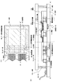
図7(A)は、発光装置の上面図であり、図7(B)は図7(A)をA−A’で切断した断面図である。点線で示された701はソース信号線駆動回路、702は画素部、703はゲート信号線駆動回路である。また、710は基板、704はカバー材、705はシール剤であり、基板710、カバー材704及びシール剤705で囲まれたところは、空間707になっている。
【0110】
なお、708はソース信号線駆動回路701及びゲート信号線駆動回路703に入力される信号を伝送するための接続配線であり、外部入力端子となるFPC(フレキシブルプリントサーキット)709からビデオ信号やクロック信号を受け取る。なお、ここではFPCしか図示されていないが、このFPCにはプリント配線基盤(PWB)が取り付けられていても良い。本明細書における発光装置には、発光装置本体だけでなく、それにFPCもしくはPWBが取り付けられた状態をも含むものとする。
【0111】
次に、断面構造について図7(B)を用いて説明する。基板710上には駆動回路及び画素部が形成されているが、ここでは、駆動回路としてソース信号線駆動回路701と画素部702が示されている。
【0112】
ここでは、ソース信号線駆動回路701はnチャネル型TFT713とpチャネル型TFT714とを組み合わせたCMOS回路が形成される。なお、駆動回路を形成するTFTは、公知のCMOS回路、PMOS回路もしくはNMOS回路で形成しても良い。また、本実施例では、基板上に駆動回路を形成したドライバー一体型を示すが、必ずしもその必要はなく、基板上ではなく外部に形成することもできる。
【0113】
また、画素部702は電流制御用TFT711とそのドレインに電気的に接続された陽極712を含む複数の画素により形成される。
【0114】
陽極712には、スリットが形成されている。また、陽極712の両端には絶縁体715が形成され、陽極712上には正孔注入層716及び正孔発生層、正孔輸送層、発光層、電子輸送層からなる有機化合物層717が形成される。さらに、絶縁体715と有機化合物層717上には陰極718が形成される。これにより、陽極、有機化合物層及び陰極からなる発光素子719が形成される。
【0115】
陰極718は全画素に共通の配線としても機能し、接続配線708を経由してFPC709に電気的に接続されている。
【0116】
また、基板710上に形成された発光素子719を封止するためにシール剤705によりカバー材704を貼り合わせる。なお、カバー材704と発光素子719との間隔を確保するために樹脂膜からなるスペーサを設けても良い。そして、シール剤705の内側の空間707には窒素等の不活性気体が充填されている。なお、シール剤705としてはエポキシ系樹脂を用いるのが好ましい。また、シール剤705はできるだけ水分や酸素を透過しない材料であることが望ましい。さらに、空間707の内部に吸湿効果をもつ物質や酸化を防止する効果をもつ物質を含有させても良い。
【0117】
また、本実施例ではカバー材704を構成する材料としてガラス基板や石英基板の他、FRP(Fiberglass-Reinforced Plastics)、PVF(ポリビニルフロライド)、マイラー、ポリエステルまたはアクリル等からなるプラスチック基板を用いることができる。
【0118】
また、シール剤705を用いてカバー材704を接着した後、さらに側面(露呈面)を覆うようにシール剤で封止することも可能である。
【0119】
以上のようにして発光素子を空間707に封入することにより、発光素子を外部から完全に遮断することができ、外部から水分や酸素といった有機化合物層の劣化を促す物質が侵入することを防ぐことができる。従って、信頼性の高い発光装置を得ることができる。
【0120】
なお、本実施例の構成は、実施例1乃至3のいずれの構成により形成された発光素子を封止して発光装置とする際に自由に組み合わせて実施することが可能である。
【0121】
[実施例5]
本発明における発光装置は、図8(A)に示す画素部とすることができる。なお、図8(A)における回路構造について図8(B)に示す。
【0122】
図8(A)において、801はスイッチング用TFTであり、nチャネル型TFTである。また、802で示される配線は、スイッチング用TFT801のゲート電極804(804a、804b)を電気的に接続するゲート配線である。
【0123】
なお、本実施例ではチャネル形成領域が二つ形成されるダブルゲート構造としているが、チャネル形成領域が一つ形成されるシングルゲート構造もしくは三つ形成されるトリプルゲート構造であっても良い。
【0124】
また、スイッチング用TFT801のソースはソース配線805に接続され、ドレインはドレイン配線806に接続される。また、ドレイン配線806は電流制御用TFT807のゲート電極808に電気的に接続される。なお、電流制御用TFT807は、pチャネル型TFTを用いて形成される。なお、本実施例ではシングルゲート構造としているが、ダブルゲート構造もしくはトリプルゲート構造であっても良い。
【0125】
また、本実施例では、スイッチング用TFT801はnチャネル型TFTで形成され、電流制御用TFT807は、Pチャネル型TFTで形成されている。しかし、スイッチング用TFT801がpチャネル型TFT、電流制御用TFT807がnチャネル型TFTで形成されても良いし、両方がnチャネル型TFTもしくはpチャネル型TFTであっても良い。
【0126】
電流制御用TFT807のソースは電流供給線809に電気的に接続され、ドレインはドレイン配線810に電気的に接続される。また、ドレイン配線810は点線で示される電極(陽極)811に電気的に接続される。なお、電極(陽極)811上に有機化合物層及び電極(陰極)を形成することにより図8(B)に示す発光素子815を形成することができる。
【0127】
また、812で示される領域には保持容量(コンデンサ)が形成される。コンデンサ812は、電流供給線809と電気的に接続された半導体膜813、ゲート絶縁膜と同一層の絶縁膜(図示せず)及びゲート電極808と電気的に接続された容量電極814との間で形成される。また、容量電極814、層間絶縁膜と同一の層(図示せず)及び電流供給線809で形成される容量も保持容量として用いることが可能である。
【0128】
なお、本実施例において説明した画素部の構成は、実施例1に示した画素部の代わりに組み合わせて実施することが可能である。
【0129】
また、本実施例は、同一基板上に画素部と、画素部の周辺に設ける駆動回路のTFT(nチャネル型TFT及びpチャネル型TFT)を同時に作製し、さらに、画素部にはTFTと電気的に接続された発光素子を形成して、素子基板を作製することもできる。
【0130】
[実施例6]
実施例1では、発光素子の光が基板を通過して下方に出射する例を示したが、本実施例では、発光素子の光が上方に出射する例を図9に示す。
【0131】
なお、本実施例の基板600としては、ガラス基板を用いるが、石英基板、シリコン基板、金属基板もしくはセラミックス基板を用いても良い。
【0132】
図9(A)において、各TFTの活性層は、少なくともチャネル形成領域、ソース領域、ドレイン領域を備えている。また、各TFTの活性層は、ゲート絶縁膜で覆われ、ゲート絶縁膜を介してチャネル形成領域と重なるゲート電極が形成されている。また、ゲート電極を覆う層間絶縁膜が設けられ、その層間絶縁膜上に各TFTのソース領域またはドレイン領域と電気的に接続する電極が設けられている。また、nチャネル型TFTである電流制御用TFT602と電気的に接続する陰極622が設けられている。また、陰極622の端部を覆いテーパー状の縁を有するように開口部を有する絶縁層623が設けられている。また、陰極622上に有機層624および正孔注入層625からなる有機化合物層が設けられ、有機化合物層上に陽極626が設けられて発光素子を形成している。なお、空間を有したまま、発光素子をカバー材で封止している。
【0133】
本実施例において、図9(B)に示す有機化合物層624、625は、実施の形態に示した方法で形成する。
【0134】
まず、実施例1に従い、層間絶縁膜上に各TFTのソース領域またはドレイン領域と電気的に接続する電極を形成した後、陰極622を形成する。陰極は、仕事関数の小さいAlや、Al:Liといったアルミニウムの合金を用いることが望ましく、陽極には透明導電膜を用い、透明導電膜としては、酸化インジウムと酸化スズとの化合物(ITOと呼ばれる)、酸化インジウムと酸化亜鉛との化合物、酸化スズまたは酸化亜鉛などを用いることが可能である。
【0135】
次いで、陰極622の端部を覆いテーパー状の縁を有するように開口部を有する絶縁層623を形成した後、陰極622上に実施の形態に示した方法で発光層624を形成する。PPVと呼ばれる材料をトルエンに分散させた組成物を窒素ガスでノズル(図示しない)から噴射させ、有機化合物層(発光層624)を70nmの膜厚で成膜する。なお、トルエンにPPVは不溶であり、この組成物は、トルエン中にPPVが分散している液体である。
【0136】
次いで、銅フタロシアニン(Cu−Pc)をトルエンに分散させた組成物を窒素ガスでノズル(図示しない)から噴射させ、有機化合物層(正孔注入層625)を20nmの膜厚で成膜する。なお、トルエンにCu−Pcは不溶であり、この組成物は、トルエン中にCu−Pcが分散している液体である。
【0137】
次いで、陽極626を形成し、この陽極626と有機化合物層624、625と、陰極622とからなる発光素子627を完成させることができる。
【0138】
本実施例により有機化合物層で生じた光を図9に示した矢印の方向に取り出す構造の発光素子を有する発光装置をすることができる。
【0139】
本実施例は、実施例2に示した低分子材料、または実施例3に示した高分子材料を用いることも可能である。
【0140】
[実施例7]
発光素子を用いた発光装置は自発光型であるため、液晶表示装置に比べ、明るい場所での視認性に優れ、視野角が広い。従って、様々な電気器具の表示部に用いることができる。
【0141】
本発明により作製した発光装置を用いた電気器具として、ビデオカメラ、デジタルカメラ、ゴーグル型ディスプレイ(ヘッドマウントディスプレイ)、ナビゲーションシステム、音響再生装置(カーオーディオ、オーディオコンポ等)、ノート型パーソナルコンピュータ、ゲーム機器、携帯情報端末(モバイルコンピュータ、携帯電話、携帯型ゲーム機または電子書籍等)、記録媒体を備えた画像再生装置(具体的にはDVD:Digital Versatile Disc)等の記録媒体を再生し、その画像を表示しうる表示装置を備えた装置)などが挙げられる。特に、斜め方向から画面を見る機会が多い携帯情報端末は、視野角の広さが重要視されるため、発光素子を有する発光装置を用いることが好ましい。それら電気器具の具体例を図10に示す。
【0142】
図10(A)は表示装置であり、筐体2001、支持台2002、表示部2003、スピーカー部2004、ビデオ入力端子2005等を含む。本発明により作製した発光装置は、表示部2003に用いることができる。発光素子を有する発光装置は自発光型であるためバックライトが必要なく、液晶表示装置よりも薄い表示部とすることができる。なお、表示装置は、パソコン用、TV放送受信用、広告表示用などの全ての情報表示用表示装置が含まれる。ちなみに図10(A)に示すディスプレイは中小型または大型のもの、例えば5〜20インチの画面サイズのものである。また、このようなサイズの表示部を形成するためには、基板の一辺が1mのものを用い、多面取りを行って量産することが好ましい。
【0143】
図10(B)はデジタルスチルカメラであり、本体2101、表示部2102、受像部2103、操作キー2104、外部接続ポート2105、シャッター2106等を含む。本発明により作製した発光装置は表示部2102に用いることができる。
【0144】
図10(C)はノート型パーソナルコンピュータであり、本体2201、筐体2202、表示部2203、キーボード2204、外部接続ポート2205、ポインティングマウス2206等を含む。本発明により作製した発光装置は表示部2203に用いることができる。
【0145】
図10(D)はモバイルコンピュータであり、本体2301、表示部2302、スイッチ2303、操作キー2304、赤外線ポート2305等を含む。本発明により作製した発光装置は表示部2302に用いることができる。
【0146】
図10(E)は記録媒体を備えた携帯型の画像再生装置(具体的にはDVD再生装置)であり、本体2401、筐体2402、表示部A2403、表示部B2404、記録媒体(DVD等)読み込み部2405、操作キー2406、スピーカー部2407等を含む。表示部A2403は主として画像情報を表示し、表示部B2404は主として文字情報を表示するが、本発明により作製した発光装置はこれら表示部A、B2403、2404に用いることができる。なお、記録媒体を備えた画像再生装置には家庭用ゲーム機器なども含まれる。
【0147】
図10(F)はゴーグル型ディスプレイ(ヘッドマウントディスプレイ)であり、本体2501、表示部2502、アーム部2503を含む。本発明により作製した発光装置は表示部2502に用いることができる。
【0148】
図10(G)はビデオカメラであり、本体2601、表示部2602、筐体2603、外部接続ポート2604、リモコン受信部2605、受像部2606、バッテリー2607、音声入力部2608、操作キー2609等を含む。本発明により作製した発光装置は表示部2602に用いることができる。
【0149】
ここで図10(H)は携帯電話であり、本体2701、筐体2702、表示部2703、音声入力部2704、音声出力部2705、操作キー2706、外部接続ポート2707、アンテナ2708等を含む。本発明により作製した発光装置は、表示部2703に用いることができる。なお、表示部2703は黒色の背景に白色の文字を表示することで携帯電話の消費電力を抑えることができる。
【0150】
なお、将来的に有機材料の発光輝度が高くなれば、出力した画像情報を含む光をレンズ等で拡大投影してフロント型若しくはリア型のプロジェクターに用いることも可能となる。
【0151】
また、上記電気器具はインターネットやCATV(ケーブルテレビ)などの電子通信回線を通じて配信された情報を表示することが多くなり、特に動画情報を表示する機会が増してきている。有機材料の応答速度は非常に高いため、発光装置は動画表示に好ましい。
【0152】
また、発光装置は発光している部分が電力を消費するため、発光部分が極力少なくなるように情報を表示することが好ましい。従って、携帯情報端末、特に携帯電話や音響再生装置のような文字情報を主とする表示部に発光装置を用いる場合には、非発光部分を背景として文字情報を発光部分で形成するように駆動することが好ましい。
【0153】
以上の様に、本発明により作製された発光装置の適用範囲は極めて広く、あらゆる分野の電気器具に用いることが可能である。また、本実施例の電気器具は実施例1〜実施例6において作製された発光装置をその表示部に用いることができる。
【0154】
【発明の効果】
本発明は、液体中の有機化合物材料がどのような状態であろうとも成膜可能な手段であり、特に溶解しにくい有機化合物材料を用いて良質な有機化合物膜を形成することを特徴とする。従って、本発明により様々な有機化合物材料を用いることが可能となり、発光装置の発光色のバリエーションを増やすことができる。
【0155】
また、本発明において、キャリアガスを用いて有機化合物を含む液体を噴射(スプレー)させて成膜を行うため、比較的短時間で成膜が可能である。また、噴射させる有機化合物を含む液体の作製方法は、非常に単純なものとすることができる。また、本発明は、所望のパターンの膜を形成する場合には、マスクを用い、さらに好ましくは電界制御によりマスクの開口部を通過させて成膜を行う。また、高価な有機化合物材料を効率よく使用するため、マスクに付着した有機化合物材料を収集し、再度利用することも可能である。
【図面の簡単な説明】
【図1】 本発明を示す図。
【図2】 本発明を示す図。
【図3】 発光装置の作製工程を示す図。
【図4】 発光装置の作製工程を示す図。
【図5】 有機化合物層の構成を示す図。
【図6】 有機化合物層の構成を示す図。
【図7】 ELモジュールの外観図を示す図。
【図8】 画素上面図を示す図。
【図9】 発光装置を示す図。
【図10】 電子機器の一例を示す図。[0001]
BACKGROUND OF THE INVENTION
The present invention uses a light-emitting element having a film containing an organic compound (hereinafter referred to as “organic compound layer”) from which fluorescence or phosphorescence can be obtained by applying an electric field, and a semiconductor element (an element using a semiconductor thin film) as a substrate. The present invention relates to a light-emitting device formed and formed typically, an EL (Electro Luminescence) display device, and an electric appliance using the EL display device as a display display (display unit). The light emitting device is also called OLED (Organic Light Emitting Diodes).
[0002]
In the present invention, the light emitting element refers to an element in which an organic compound layer is provided between a pair of electrodes, and the light emitting device refers to an image display device or a light emitting device using the light emitting element. Also, connectors with light emitting elements such as anisotropic conductive film (FPC: Flexible Printed Circuit) or TAB (Tape Automated Bonding) tape or TCP (Tape Carrier Package) attached, printed wiring on the end of TAB tape or TCP It is assumed that the light-emitting device also includes a module provided with a plate or a module in which an IC (integrated circuit) is directly mounted on a light-emitting element by a COG (Chip On Glass) method.
[0003]
[Prior art]
In recent years, a light emitting device (EL display device) using an EL element as a light emitting element utilizing an EL (Electro Luminescence) phenomenon of a light emitting organic material has been developed. The EL display device is considered to be superior to the conventional liquid crystal display device in that the viewing angle is wide and the visibility is excellent.
[0004]
There are two types of EL display devices, a passive type (simple matrix type) and an active type (active matrix type), both of which are actively developed. In particular, active matrix EL display devices are currently attracting attention. In addition, as an organic compound material that becomes an EL layer (strictly speaking, a light emitting layer) that can be said to be the center of an EL element, a low molecular organic compound material and a high molecular (polymer) organic compound material have been studied.
[0005]
As a method for forming these organic compound materials, methods such as an inkjet method, a vapor deposition method, and a spin coating method are known.
[0006]
However, considering the production of full-color flat panel displays using red, green, and blue emission colors, none of the above film formation methods can be called an optimum film formation method in various respects, and is inexpensive. It was a problem in mass production.
[0007]
[Problems to be solved by the invention]
Therefore, the present invention provides means for forming a film made of an organic compound material at low cost using an organic compound material having high luminous efficiency.
[0008]
Moreover, since the organic compound material generally used for a light emitting element is expensive, it is desired to use it as efficiently as possible.
[0009]
[Means for Solving the Problems]
The present invention is characterized in that a film containing an organic compound aggregate is formed on a substrate in an inert gas atmosphere by spray injection using a colloidal solution (also called a sol) in which the organic compound aggregate is dispersed. Yes. In the present invention, the organic compound is present as particles in which several organic compounds are aggregated in a liquid.
[0010]
Conventionally, a solution is prepared by dissolving an organic compound material in a solvent having high solubility in the organic compound material, and a film is formed by an inkjet method or a spin coating method.
[0011]
Therefore, in the conventional film forming method, an organic compound material having a high solubility is preferred and used. In addition, for organic compound materials with low solubility, the molecular structure was introduced with substituents in order to improve solubility, and the solubility was improved. However, by introducing substituents, the color purity was lowered and light emission was further achieved. The color has also changed. For example, the organic compound material represented by PPV (1,4-polyphenylene vinylene) emits green light, but RO-PPV (2,5-dialkoxy-1, The organic compound material represented by 4-phenylenevinylene has an orange emission color.
[0012]
Among other organic compound materials, materials that can convert triplet excitation energy into light emission, such as metal complexes with platinum as the central metal (hereinafter also referred to as platinum complexes), metal complexes with iridium as the central metal ( Hereinafter, the iridium complex) is mixed with a plurality of other organic compound materials and a solvent as a dopant, so that it is difficult to synthesize by adjusting the ratio of each to the whole.
[0013]
The present invention is a means capable of forming a film regardless of the state of the organic compound material in the liquid, and is characterized in that a high-quality organic compound film is formed using an organic compound material that is particularly difficult to dissolve. . In the present invention, a film containing an organic compound is ejected (sprayed) using a carrier gas, so that the film can be formed in a short time. In addition, a method for manufacturing a liquid containing an organic compound to be ejected can be very simple. In the present invention, when a film having a desired pattern is formed, the film is formed by using a mask and passing through the opening of the mask. Further, in order to efficiently use an expensive organic compound material, the organic compound material attached to the mask can be collected and reused.
[0014]
The structure related to the manufacturing method of the invention disclosed in this specification is as follows.
Light emission characterized by forming a film containing an aggregate of organic compounds by spraying a composition in which an aggregate of organic compounds is dispersed particles and a dispersion medium is liquid from a nozzle with an inert gas and spraying the adherend It is a manufacturing method of an apparatus.
[0015]
Moreover, in order to control the formation position of the film | membrane containing the aggregate | assembly of the said organic compound, other structures,
A composition in which an aggregate of organic compounds is dispersed particles and a dispersion medium is liquid is sprayed from a nozzle with an inert gas, and is passed through an opening of a mask disposed between the nozzle and the adherend to the adherend. A method for manufacturing a light-emitting device is characterized in that a film containing an aggregate of organic compounds is formed by spraying.
[0016]
In the above structure, the composition or the mask may be charged in order to control the formation position of the film containing the aggregate of organic compounds.
[0017]
In each of the above structures, the composition is a liquid having fluidity, and an aggregate of organic compounds is dispersed as colloidal particles in the liquid.
[0018]
In each of the above structures, the organic compound is one or more selected from quinacridone, tris (2-phenylpyridine) iridium, and bathocuproine.
[0019]
In each of the above structures, the organic compound includes poly (1,4-phenylene vinylene), poly (1,4-naphthalene vinylene), poly (2-phenyl-1,4-phenylene vinylene), polythiophene, poly ( It is characterized by being one kind or plural kinds selected from 3-phenylthiophene), poly (1,4-phenylene) and poly (2,7-fluorene).
[0020]
In the present invention, the organic compound may be a particle in which several organic compounds are aggregated in a liquid, or may be an organic compound that is partially dissolved in the liquid.
Therefore, a composition in which an organic compound is dissolved in a liquid may be sprayed on an adherend to form a film containing the organic compound.
A method for manufacturing a light-emitting device, wherein a composition in which an organic compound is dissolved in a liquid is sprayed onto an adherend by spraying with an inert gas from a nozzle to form a film containing the organic compound.
[0021]
In another configuration, in order to control the formation position of the film containing the organic compound, a composition in which the organic compound is dissolved in the liquid is injected from the nozzle with an inert gas, and is disposed between the nozzle and the adherend. A method for manufacturing a light-emitting device is characterized in that a film containing an organic compound is formed by passing through an opening of a mask and spraying on an adherend.
[0022]
Further, the composition or the mask may be charged in order to control the formation position of the film containing the organic compound.
[0023]
Note that in the above structure, the composition is a fluid liquid, and at least a part of the organic compound is dissolved in the liquid.
[0024]
In each of the above structures, the liquid is one or more selected from alcohols, toluene, and water.
[0025]
In each of the above structures, the film is formed in an inert gas atmosphere.
[0026]
Moreover, in each said structure, the injection port of the said nozzle is characterized by being 1 or 2 or more.
[0027]
In each of the above configurations, the adherend is a substrate provided with a switching element.
[0028]
In each of the above configurations, a film may be formed on the adherend while moving the adherend, or a film may be formed on the adherend while moving the nozzle.
[0029]
In each of the above structures, an electric field may be generated between the nozzle and the adherend in order to control the position where the film is formed.
[0030]
DETAILED DESCRIPTION OF THE INVENTION
Embodiments of the present invention will be described below.
[0031]
FIG. 2A is a simplified diagram of the present invention.
[0032]
In FIG. 2A, a
[0033]
Note that here, an iridium complex, which is a low-molecular material with high emission efficiency, typically, tris (2-phenylpyridine) iridium is used as the organic compound. The molecular formula of this iridium complex is shown below.
[0034]
[Chemical 1]
In the present invention, the iridium complex or aggregate thereof and bathocuproine (hereinafter referred to as BCP) are dispersed in colloidal particles in a liquid of toluene or alcohols.
[0036]
On the other hand, when the coating method is used, 2- (4-biphenyl) -5- (4-tert-butylphenyl) -1,3,4-oxadiazole (referred to as PBD) and poly (N--) with toluene as a solvent. A coating solution was prepared by dispersing several wt% of an iridium complex as a dopant in a liquid in which vinyl carbazole (called PVK) was dissolved at a certain ratio, but it was difficult to prepare this coating solution. The liquid 204 of the present invention can be obtained easily in a short time.
[0037]
The
[0038]
As another ejection method, a liquid is moved from a container by a compressed gas source (not shown), a carrier gas is flowed toward the nozzle outlet, and a spray composed of liquid and gas is formed and discharged in the chamber. A method may be used. These parts are self-evident and are not shown in detail here. Moreover, you may provide the apparatus which controls the flow volume of a liquid.
[0039]
As another ejection method, as shown in FIG. 2 (B), the pressure of the tube from the container to the nozzle is increased by a
[0040]
Further, as shown in FIG. 2C, it is preferable that the organic compound is uniformly dispersed in the liquid. In the pipe connecting the container and the spout, the
[0041]
Of the liquid ejected by any one of the above ejecting methods, the liquid that has passed through the opening of the mask adheres to the
[0042]
A desired pattern can also be obtained by moving the substrate in the X direction or the Y direction while intermittently or continuously performing the injection as described above. It is also possible to obtain a desired pattern by fixing the substrate and scanning the nozzle in the X direction or the Y direction.
[0043]
Further, a substrate heater in contact with the substrate may be provided to heat the substrate during film formation. In the present invention, the surface temperature of the substrate may be room temperature to 200 ° C.
[0044]
Further, when the
[0045]
Here, an iridium complex has been described as an example. However, the present invention is not limited to other low molecular weight materials (such as quinacridone and bathocuproine), and further high molecular weight materials (poly (1,4-phenylene vinylene), poly (1,4-naphthalene vinylene). ), Poly (2-phenyl-1,4-phenylenevinylene), polythiophene, poly (3-phenylthiophene), poly (1,4-phenylene), poly (2,7-fluorene), etc.) Is possible.
[0046]
For simplification, FIG. 2 does not show a substrate holder for fixing the substrate or a holder for fixing the mask.
[0047]
In addition, here, an example in which the
[0048]
FIG. 1 shows an example in which a plurality is provided. In FIG. 1, six jet nozzles are provided and passed through a line-shaped
[0049]
The atmosphere in the chamber 100 is a nitrogen atmosphere, and a liquid 104 containing an organic compound is ejected from the nozzle 103 with an inert gas, and passes through an
[0050]
In FIG. 1, the nozzle is moved in the Y direction (direction perpendicular to the water surface). Moreover, you may move to a X direction (direction parallel to a water surface).
[0051]
This device is also suitable for mass production. Here, the mask is provided with a slit-shaped opening, but the shape is not particularly limited. The mask may be designed as appropriate.
[0052]
The present invention having the above-described configuration will be described in more detail with the following examples.
[0053]
(Example)
[Example 1]
In this embodiment, a method for manufacturing a pixel portion of a light-emitting device will be described with reference to FIGS. In this embodiment, a case where a thin film transistor (TFT) is formed as a semiconductor element will be described.
[0054]
First, a crystalline silicon film is formed to a thickness of 50 nm on a light-transmitting
[0055]
Next, as shown in FIG. 3B, an element (typically boron) belonging to Group 13 of the periodic table is added using the
[0056]
Next, a protective film (here, a silicon nitride film) 315 is formed to a thickness of 50 nm, and then heat treatment is performed to activate the elements belonging to Group 13 of the periodic table added. This activation may be performed by furnace annealing, laser annealing or lamp annealing, or a combination thereof. In this embodiment, heat treatment is performed at 500 ° C. for 4 hours in a nitrogen atmosphere.
[0057]
When the activation is completed, it is effective to perform a hydrogenation treatment. For the hydrogenation treatment, a known hydrogen annealing technique or plasma hydrogenation technique may be used.
[0058]
Next, as shown in FIG. 3C, a first
[0059]
Next, a second
[0060]
Thereafter, a resist mask having a desired pattern is formed, a contact hole reaching the drain region of the TFT is formed, and wirings 318 to 321 are formed. As a wiring material, an alloy metal other than Al and Ti as a conductive metal film may be used to form a film by a sputtering method or a vacuum evaporation method, and then patterned into a desired shape.
[0061]
In this state, the TFT is completed. In this embodiment mode, a switching
[0062]
At the same time, a storage capacitor is formed. The storage capacitor includes a semiconductor layer formed simultaneously with the active layer of the TFT, a lower storage capacitor formed by a wiring that forms a gate insulating film and a gate electrode, a wiring that forms a gate electrode, a protective film, and a first interlayer insulating film And an upper storage capacitor formed by the second interlayer insulating film and the current supply line. The semiconductor layer is electrically connected to the current supply line.
[0063]
Next, a light-transmitting conductive film which is an anode of the light-emitting element, here, an ITO film is formed. Further, as the conductive film, a material having a work function larger than that of the material forming the cathode is used, and further, a material having a sheet resistance lower than that of the ITO film, specifically, platinum (Pt), chromium (Cr), tungsten (W ) Or a material such as nickel (Ni). Note that the film thickness of the conductive film at this time is preferably 0.1 to 1 μm. Subsequently, as illustrated in FIG. 3D, the conductive film is etched to form the
[0064]
Thereafter, an organic resin film made of polyimide, acrylic, or polyimide amide is formed on the entire surface. For these, a thermosetting material that is cured by heating or a photosensitive material that is cured by irradiation with ultraviolet rays can be employed. When a thermosetting material is used, a resist mask is formed thereafter, and an insulating
[0065]
Next, an organic compound layer is formed over the
[0066]
First, the organic compound layer (hole injection layer 324a) is formed to a thickness of 15 nm on the
[0067]
Next, an iridium complex, which is a light-emitting organic compound, tris (2-phenylpyridine) iridium (Ir (ppy)Three) And bathocuproin (BCP), which is an organic compound serving as a host (hereinafter referred to as host material), in toluene, as shown in FIG. 3 (E), from a nozzle (not shown) with nitrogen gas. The organic compound layer (light emitting layer 324c) is formed to a thickness of 25 to 40 nm by spraying. Here, an organic compound layer is selectively formed using the
[0068]
Further, a composition in which bathocuproin (BCP), which is a blocking organic compound, is dispersed in toluene is sprayed from a nozzle with nitrogen gas as shown in FIG. 3 (E), and the organic compound layer (blocking layer 324d) is 8 nm. The film is formed with a film thickness.
[0069]
Next, tris (8-quinolinolato) aluminum (hereinafter referred to as Alq), which is an organic compound having an electron transport property by a coating method or a vapor deposition method.ThreeAnd an organic compound layer (electron transport layer 325) is formed to a film thickness of 25 nm.
[0070]
Here, the case where the organic compound layer that emits green light is formed using five kinds of organic compounds having different functions has been described. However, the present invention is not limited thereto, and is known as an organic compound that emits green light. Materials can be used.
[0071]
Thus, in this example, among these organic compound layers, an example in which only the light emitting layer and the blocking layer were formed by the method described in the embodiment was shown, but the present invention is not limited thereto, At least one layer or all organic compound layers may be formed by the method described in the embodiment.
[0072]
Next, the
[0073]
As described above, a light-emitting element including the
[0074]
FIG. 5B illustrates the case where all the organic compound layers are formed by the method described in the embodiment mode. In FIG. 5B, the same reference numerals are used for portions corresponding to those in FIGS. Here, the procedure for forming the green organic compound layer will be described.
[0075]
In FIG. 5B, on the anode 322Organic compound layer 327Only provided,Organic compound layer 327The light-emitting element is provided with a
[0076]
Next, as illustrated in FIG. 4C, the light-emitting element is sealed with a
[0077]
In addition to a glass substrate or a quartz substrate, a plastic substrate made of FRP (Fiberglass-Reinforced Plastics), PVF (polyvinyl fluoride), Mylar, polyester, acrylic, or the like can be used as a material for forming the
[0078]
[Example 2]
In Example 1, an example in which an iridium complex, which is a low molecular material, is used as the organic compound has been shown. However, in the present invention, the following polymer materials can be used for the light emitting layer. Note that this embodiment has the same configuration as the first embodiment except for the organic compound layer, and detailed description thereof is omitted here for the sake of brevity. The same parts as those in the first embodiment will be described using the same reference numerals as those in FIGS.
[0079]
First, according to Example 1, the steps up to immediately before the formation of the organic compound layer are performed.
[0080]
Next, the hole injection layer 524 is formed over the
[0081]
Next, the light-emitting layer 525 is formed over the hole-injection layer 524 by the method described in Embodiment Mode.
[0082]
Here, a material called PPV, poly (1,4-phenylene vinylene), can be used for the light-emitting layer. The molecular formula is shown below.
[0083]
[Formula 2]
A composition in which PPV is dispersed in toluene is sprayed from a nozzle (not shown) with nitrogen gas to form an organic compound layer (light emitting layer 525) with a thickness of 70 nm. In addition, PPV is insoluble in toluene, and this composition is a liquid in which PPV is dispersed in toluene. Further, in this example, when forming the light emitting layer, the composition is appropriately selected so that the hole injection layer is not dissolved.
[0085]
In the subsequent steps, the
[0086]
Incidentally, in conventional methods, typically coating methods, organic compound materials having high solubility are preferred and used, and RO-PPV (2,5-dialkoxy) into which an alkoxy substituent is introduced to improve solubility. An organic compound material represented by (-1,4-phenylene vinylene) has been used. For this reason, the color purity was lowered, and the emission color was also changed. The emission color of this RO-PPV is an orange emission color.
[0087]
Further, instead of the PPV, a material called PNV, poly (1,4-naphthalene vinylene) can be used. The molecular formula is shown below.
[0088]
[Formula 3]
In addition, a material called phenyl-PPV, poly (2-phenyl-1,4-phenylenevinylene) can be used. The molecular formula is shown below.
[0090]
[Formula 4]
Further, it is possible to use a material called PT, polythiophene. The molecular formula is shown below.
[0092]
[Formula 5]
In addition, a material called PPT, poly (3-phenylthiophene) can be used. The molecular formula is shown below.
[0094]
[Formula 6]
Further, a material called PPP, poly (1,4-phenylene) can be used. The molecular formula is shown below.
[0096]
[Formula 7]
In addition, a material called PF, poly (2,7-fluorene) can be used. The molecular formula is shown below.
[0098]
[Formula 8]
Two or more of the above materials may be combined.
[0100]
Note that these materials are merely examples, and are not particularly limited. These materials are insoluble in toluene and alcohols.
[0101]
[Example 3]
In Example 1, an example in which an iridium complex that is a low molecule is used as the organic compound is shown, but the present invention can use other molecular materials shown below for the light emitting layer.
[0102]
Instead of the iridium complex of Example 1, a material called quinacridone can be used. The molecular formula is shown below.
[0103]
[Formula 9]
Further, in place of the iridium complex of Example 1, a material called BCP, bathocuproine, can be used. The molecular formula is shown below.
[0105]
[Formula 10]
Two or more of the above materials may be combined.
[0107]
These materials are insoluble in toluene and alcohols.
[0108]
[Example 4]
In this embodiment, an external view of a light emitting device of the present invention will be described with reference to FIG.
[0109]
7A is a top view of the light-emitting device, and FIG. 7B is a cross-sectional view taken along line A-A ′ in FIG. 7A. 701 indicated by a dotted line is a source signal line driver circuit, 702 is a pixel portion, and 703 is a gate signal line driver circuit. Reference numeral 710 denotes a substrate, reference numeral 704 denotes a cover material, and reference numeral 705 denotes a sealant. A space 707 is surrounded by the substrate 710, the cover material 704, and the sealant 705.
[0110]
Reference numeral 708 denotes a connection wiring for transmitting signals input to the source signal line driver circuit 701 and the gate signal line driver circuit 703, and a video signal or a clock signal from an FPC (flexible printed circuit) 709 serving as an external input terminal. Receive. Although only the FPC is shown here, a printed wiring board (PWB) may be attached to the FPC. The light-emitting device in this specification includes not only a light-emitting device body but also a state in which an FPC or a PWB is attached thereto.
[0111]
Next, a cross-sectional structure will be described with reference to FIG. A driver circuit and a pixel portion are formed over the substrate 710. Here, a source signal line driver circuit 701 and a pixel portion 702 are shown as the driver circuits.
[0112]
Here, as the source signal line driver circuit 701, a CMOS circuit in which an n-
[0113]
The pixel portion 702 is formed by a plurality of pixels including a
[0114]
A slit is formed in the anode 712. In addition, an insulator 715 is formed on both ends of the anode 712, and an
[0115]
The
[0116]
In addition, a cover material 704 is attached with a sealant 705 to seal the light-emitting element 719 formed over the substrate 710. Note that a spacer made of a resin film may be provided in order to secure a space between the cover material 704 and the light emitting element 719. A space 707 inside the sealing agent 705 is filled with an inert gas such as nitrogen. Note that an epoxy resin is preferably used as the sealant 705. In addition, the sealant 705 is desirably a material that does not transmit moisture and oxygen as much as possible. Further, a substance having a hygroscopic effect or a substance having an effect of preventing oxidation may be contained in the space 707.
[0117]
In this embodiment, a plastic substrate made of FRP (Fiberglass-Reinforced Plastics), PVF (polyvinyl fluoride), Mylar, polyester, acrylic, or the like is used as a material constituting the cover material 704 in addition to a glass substrate or a quartz substrate. Can do.
[0118]
Further, after the cover material 704 is bonded using the sealant 705, the cover material 704 can be further sealed with a sealant so as to cover the side surface (exposed surface).
[0119]
By encapsulating the light emitting element in the space 707 as described above, the light emitting element can be completely blocked from the outside, and a substance that promotes deterioration of the organic compound layer such as moisture and oxygen can be prevented from entering from the outside. Can do. Therefore, a highly reliable light-emitting device can be obtained.
[0120]
Note that the structure of this embodiment can be freely combined when the light-emitting element formed by any structure of Embodiments 1 to 3 is sealed to form a light-emitting device.
[0121]
[Example 5]
The light-emitting device of the present invention can be a pixel portion illustrated in FIG. Note that the circuit structure in FIG. 8A is illustrated in FIG.
[0122]
In FIG. 8A,
[0123]
Note that although a double gate structure in which two channel formation regions are formed is used in this embodiment, a single gate structure in which one channel formation region is formed or a triple gate structure in which three channel formation regions are formed may be used.
[0124]
The source of the switching
[0125]
In this embodiment, the switching
[0126]
The source of the
[0127]
In addition, a storage capacitor (capacitor) is formed in a region indicated by 812. The
[0128]
Note that the structure of the pixel portion described in this embodiment can be implemented in combination instead of the pixel portion described in Embodiment 1.
[0129]
In this embodiment, a pixel portion and TFTs (n-channel TFT and p-channel TFT) of a driver circuit provided around the pixel portion are formed on the same substrate at the same time. An element substrate can also be manufactured by forming connected light emitting elements.
[0130]
[Example 6]
In the first embodiment, an example in which the light from the light emitting element is emitted downward through the substrate is shown, but in this embodiment, an example in which the light from the light emitting element is emitted upward is shown in FIG.
[0131]
A glass substrate is used as the
[0132]
In FIG. 9A, the active layer of each TFT includes at least a channel formation region, a source region, and a drain region. The active layer of each TFT is covered with a gate insulating film, and a gate electrode is formed so as to overlap the channel formation region via the gate insulating film. An interlayer insulating film that covers the gate electrode is provided, and an electrode that is electrically connected to the source region or drain region of each TFT is provided on the interlayer insulating film. Further, a
[0133]
In this example, the organic compound layers 624 and 625 illustrated in FIG. 9B are formed by the method described in Embodiment Mode.
[0134]
First, in accordance with Embodiment 1, an electrode electrically connected to the source region or drain region of each TFT is formed on the interlayer insulating film, and then the
[0135]
Next, an insulating
[0136]
Next, a composition in which copper phthalocyanine (Cu—Pc) is dispersed in toluene is sprayed from a nozzle (not shown) with nitrogen gas to form an organic compound layer (hole injection layer 625) with a thickness of 20 nm. Note that Cu-Pc is insoluble in toluene, and this composition is a liquid in which Cu-Pc is dispersed in toluene.
[0137]
Next, an
[0138]
In this embodiment, a light-emitting device having a light-emitting element having a structure in which light generated in the organic compound layer is extracted in the direction of the arrow illustrated in FIG. 9 can be obtained.
[0139]
In this embodiment, the low molecular material shown in Embodiment 2 or the polymer material shown in Embodiment 3 can be used.
[0140]
[Example 7]
Since a light-emitting device using a light-emitting element is a self-luminous type, it is superior in visibility in a bright place and has a wide viewing angle as compared with a liquid crystal display device. Therefore, it can be used for display portions of various electric appliances.
[0141]
As an electric appliance using a light emitting device manufactured according to the present invention, a video camera, a digital camera, a goggle type display (head mounted display), a navigation system, a sound reproduction device (car audio, audio component, etc.), a notebook personal computer, a game Play back a recording medium such as a device, a portable information terminal (mobile computer, mobile phone, portable game machine or electronic book), an image playback device (specifically a DVD: Digital Versatile Disc) provided with the recording medium, And a device provided with a display device capable of displaying an image). In particular, a portable information terminal that frequently sees a screen from an oblique direction emphasizes the wide viewing angle, and thus a light emitting device having a light emitting element is preferably used. Specific examples of these electric appliances are shown in FIG.
[0142]
FIG. 10A illustrates a display device, which includes a
[0143]
FIG. 10B shows a digital still camera, which includes a
[0144]
FIG. 10C illustrates a laptop personal computer, which includes a
[0145]
FIG. 10D illustrates a mobile computer, which includes a
[0146]
FIG. 10E illustrates a portable image reproducing device (specifically, a DVD reproducing device) provided with a recording medium, which includes a
[0147]
FIG. 10F illustrates a goggle type display (head mounted display), which includes a
[0148]
FIG. 10G illustrates a video camera, which includes a main body 2601, a
[0149]
Here, FIG. 10H shows a mobile phone, which includes a
[0150]
If the emission luminance of the organic material is increased in the future, the light including the output image information can be enlarged and projected by a lens or the like and used for a front type or rear type projector.
[0151]
In addition, the electric appliances often display information distributed through electronic communication lines such as the Internet or CATV (cable television), and in particular, opportunities to display moving image information are increasing. Since the response speed of the organic material is very high, the light-emitting device is preferable for displaying moving images.
[0152]
In addition, since the light emitting portion of the light emitting device consumes power, it is preferable to display information so that the light emitting portion is minimized. Therefore, when a light emitting device is used for a display unit mainly including character information, such as a portable information terminal, particularly a mobile phone or a sound reproduction device, it is driven so that character information is formed by the light emitting part with the non-light emitting part as the background. It is preferable to do.
[0153]
As described above, the applicable range of the light-emitting device manufactured according to the present invention is so wide that the light-emitting device can be used for electric appliances in various fields. In addition, the electric appliance of this embodiment can use the light emitting device manufactured in Embodiments 1 to 6 for the display portion.
[0154]
【The invention's effect】
The present invention is a means capable of forming a film regardless of the state of the organic compound material in the liquid, and is characterized in that a high-quality organic compound film is formed using an organic compound material that is particularly difficult to dissolve. . Therefore, various organic compound materials can be used according to the present invention, and variations in emission color of the light emitting device can be increased.
[0155]
In the present invention, since a film containing an organic compound is ejected (sprayed) using a carrier gas, the film can be formed in a relatively short time. In addition, a method for manufacturing a liquid containing an organic compound to be ejected can be very simple. In the present invention, when a film having a desired pattern is formed, the mask is used, and more preferably, the film is formed by passing through the opening of the mask by electric field control. Further, in order to efficiently use an expensive organic compound material, the organic compound material attached to the mask can be collected and reused.
[Brief description of the drawings]
FIG. 1 shows the present invention.
FIG. 2 shows the present invention.
3A and 3B illustrate a manufacturing process of a light-emitting device.
4A and 4B illustrate a manufacturing process of a light-emitting device.
FIG. 5 is a diagram showing a configuration of an organic compound layer.
FIG. 6 shows a structure of an organic compound layer.
FIG. 7 shows an external view of an EL module.
FIG. 8 is a diagram showing a top view of a pixel.
FIG 9 illustrates a light-emitting device.
FIG 10 illustrates an example of an electronic device.
Claims (9)
且つ、噴射された前記組成物を、前記ノズルと電極との間で帯電させ、
前記噴射された前記組成物を、前記ノズルと前記電極上との間に配置されたマスクの開口部を通過させて、前記電極上に有機化合物を含む膜を形成することを特徴とする発光装置の作製方法。A composition composed of dispersed particles composed of an organic compound and a dispersion medium is sprayed with an inert gas from a nozzle,
And charging the jetted composition between the nozzle and the electrode,
The injected the composition, the is passed through the opening of the placement mask between the nozzle and on the electrode, the light emitting device and forming a film containing an organic compound on the electrode Manufacturing method.
前記分散媒は流動性を有する液体であり、前記分散媒中に前記有機化合物がコロイド粒子として分散していることを特徴とする発光装置の作製方法。In claim 1 ,
The dispersion medium is a liquid having fluidity, a method for manufacturing a light emitting device, wherein the organic compound in the dispersion medium are dispersed as colloidal particles.
前記分散媒としては、アルコール類、トルエン、水から選ばれた1種または複数種を用いることを特徴とする発光装置の作製方法。In claim 1 or claim 2 ,
As the dispersion medium, one or a plurality of types selected from alcohols, toluene, and water are used.
且つ、噴射された前記組成物を、前記ノズルと電極との間で帯電させ、
前記噴射された前記組成物を、前記ノズルと前記電極上との間に配置されたマスクの開口部を通過させて、前記電極上に有機化合物を含む膜を形成することを特徴とする発光装置の作製方法。A composition in which an organic compound is dissolved in a liquid is jetted with an inert gas from a nozzle,
And charging the jetted composition between the nozzle and the electrode,
The injected the composition, the is passed through the opening of the placement mask between the nozzle and on the electrode, the light emitting device and forming a film containing an organic compound on the electrode Manufacturing method.
前記組成物は流動性を有する液体であり、前記組成物中に前記有機化合物の少なくとも一部が溶解していることを特徴とする発光装置の作製方法。In claim 4 ,
The composition is a liquid having fluidity, a method for manufacturing a light emitting device and at least a part of said organic compounds in the composition is dissolved.
前記液体としては、アルコール類、トルエン、水から選ばれた1種または複数種を用いることを特徴とする発光装置の作製方法。In claim 4 or claim 5 ,
As the liquid, one or a plurality of types selected from alcohols, toluene, and water are used.
前記マスクを帯電させることを特徴とする発光装置の作製方法。A method for manufacturing a light-emitting device, wherein the mask is charged.
前記有機化合物は、キナクリドン、トリス(2−フェニルピリジン)イリジウム、バソキュプロインから選ばれた1種または複数種を用いることを特徴とする発光装置の作製方法。In any one of Claims 1 thru | or 7 ,
The method for manufacturing a light-emitting device is characterized in that the organic compound is one or more selected from quinacridone, tris (2-phenylpyridine) iridium, and bathocuproine.
前記有機化合物は、ポリ(1,4−フェニレンビニレン)、ポリ(1,4−ナフタレンビニレン)、ポリ(2−フェニル−1,4−フェニレンビニレン)、ポリチオフェン、ポリ(3−フェニルチオフェン)、ポリ(1,4−フェニレン)、ポリ(2,7−フルオレン)から選ばれた1種または複数種を用いることを特徴とする発光装置の作製方法。In any one of claims 1乃optimum claim 8,
The organic compound includes poly (1,4-phenylene vinylene), poly (1,4-naphthalene vinylene), poly (2-phenyl-1,4-phenylene vinylene), polythiophene, poly (3-phenylthiophene), poly A method for manufacturing a light-emitting device, using one or more selected from (1,4-phenylene) and poly (2,7-fluorene).
Priority Applications (5)
| Application Number | Priority Date | Filing Date | Title |
|---|---|---|---|
| JP2001151572A JP3969698B2 (en) | 2001-05-21 | 2001-05-21 | Method for manufacturing light emitting device |
| TW091109010A TW541727B (en) | 2001-05-21 | 2002-04-30 | Light emitting device and method of manufacturing thereof |
| US10/147,923 US7179756B2 (en) | 2001-05-21 | 2002-05-20 | Light emitting device and method of manufacturing thereof |
| CNB021203024A CN100452474C (en) | 2001-05-21 | 2002-05-21 | Luminous device and method for making same |
| US11/707,099 US7485584B2 (en) | 2001-05-21 | 2007-02-16 | Light emitting device and method of manufacturing thereof |
Applications Claiming Priority (1)
| Application Number | Priority Date | Filing Date | Title |
|---|---|---|---|
| JP2001151572A JP3969698B2 (en) | 2001-05-21 | 2001-05-21 | Method for manufacturing light emitting device |
Publications (3)
| Publication Number | Publication Date |
|---|---|
| JP2002343566A JP2002343566A (en) | 2002-11-29 |
| JP2002343566A5 JP2002343566A5 (en) | 2005-09-08 |
| JP3969698B2 true JP3969698B2 (en) | 2007-09-05 |
Family
ID=18996396
Family Applications (1)
| Application Number | Title | Priority Date | Filing Date |
|---|---|---|---|
| JP2001151572A Expired - Fee Related JP3969698B2 (en) | 2001-05-21 | 2001-05-21 | Method for manufacturing light emitting device |
Country Status (4)
| Country | Link |
|---|---|
| US (2) | US7179756B2 (en) |
| JP (1) | JP3969698B2 (en) |
| CN (1) | CN100452474C (en) |
| TW (1) | TW541727B (en) |
Families Citing this family (25)
| Publication number | Priority date | Publication date | Assignee | Title |
|---|---|---|---|---|
| JP3969698B2 (en) * | 2001-05-21 | 2007-09-05 | 株式会社半導体エネルギー研究所 | Method for manufacturing light emitting device |
| US7199515B2 (en) * | 2001-06-01 | 2007-04-03 | Semiconductor Energy Laboratory Co., Ltd. | Organic light emitting element and light emitting device using the element |
| US20020197393A1 (en) * | 2001-06-08 | 2002-12-26 | Hideaki Kuwabara | Process of manufacturing luminescent device |
| US7112113B2 (en) * | 2002-12-25 | 2006-09-26 | Semiconductor Energy Laboratory Co., Ltd. | Manufacturing method of display device |
| WO2004064453A1 (en) * | 2003-01-10 | 2004-07-29 | Semiconductor Energy Laboratory Co., Ltd. | Light emitting element and process for preparing the same |
| US7211461B2 (en) * | 2003-02-14 | 2007-05-01 | Semiconductor Energy Laboratory Co., Ltd. | Manufacturing apparatus |
| JP4799176B2 (en) * | 2003-07-24 | 2011-10-26 | 株式会社半導体エネルギー研究所 | Method for manufacturing light emitting device |
| KR100656497B1 (en) * | 2004-02-09 | 2006-12-11 | 삼성에스디아이 주식회사 | Organic light-emitting dispaly and fabrication method of the same |
| US7749037B2 (en) * | 2004-02-19 | 2010-07-06 | E. I. Du Pont De Nemours And Company | Process for fabricating an organic electronic device using liquid deposition and devices made by the process |
| JP4792724B2 (en) * | 2004-09-29 | 2011-10-12 | コニカミノルタホールディングス株式会社 | Organic electroluminescence element, display device and lighting device |
| US9734901B2 (en) * | 2004-10-29 | 2017-08-15 | Semiconductor Energy Laboratory Co., Ltd. | Display device with semiconductor memory cell |
| US8986780B2 (en) * | 2004-11-19 | 2015-03-24 | Massachusetts Institute Of Technology | Method and apparatus for depositing LED organic film |
| JP2008104894A (en) * | 2005-02-14 | 2008-05-08 | Pioneer Electronic Corp | Process and equipment for production of material coated with coating material and surface mask |
| JPWO2006085456A1 (en) * | 2005-02-14 | 2008-08-07 | パイオニア株式会社 | Method and apparatus for manufacturing coated material |
| JP5079215B2 (en) * | 2005-03-04 | 2012-11-21 | パイオニア株式会社 | Manufacturing method of coating liquid coating material |
| JP5134193B2 (en) * | 2005-07-15 | 2013-01-30 | 株式会社東芝 | Semiconductor device and manufacturing method thereof |
| KR101097927B1 (en) * | 2005-08-18 | 2011-12-23 | 재단법인서울대학교산학협력재단 | Method for Manufacturig a Liquid Crystal Display Device |
| US7432187B1 (en) * | 2007-05-14 | 2008-10-07 | Eastman Kodak Company | Method for improving current distribution of a transparent electrode |
| US20090042122A1 (en) * | 2007-08-08 | 2009-02-12 | Katun Corporation | Methods of producing toner compositions and toner compositions produced therefrom |
| EP2211374A4 (en) * | 2007-11-16 | 2012-10-10 | Ulvac Inc | Substrate processing method and substrate processed by this method |
| JP5416987B2 (en) | 2008-02-29 | 2014-02-12 | 株式会社半導体エネルギー研究所 | Film forming method and light emitting device manufacturing method |
| US20090218219A1 (en) * | 2008-02-29 | 2009-09-03 | Semiconductor Energy Laboratory Co., Ltd. | Manufacturing Apparatus |
| JP5238544B2 (en) | 2008-03-07 | 2013-07-17 | 株式会社半導体エネルギー研究所 | Film forming method and light emitting device manufacturing method |
| US8409672B2 (en) * | 2008-04-24 | 2013-04-02 | Semiconductor Energy Laboratory Co., Ltd. | Method of manufacturing evaporation donor substrate and method of manufacturing light-emitting device |
| KR101084277B1 (en) * | 2010-02-03 | 2011-11-16 | 삼성모바일디스플레이주식회사 | Organic Light Emitting Diode Display Device and Fabricating method of the same |
Family Cites Families (80)
| Publication number | Priority date | Publication date | Assignee | Title |
|---|---|---|---|---|
| US4617195A (en) * | 1984-03-26 | 1986-10-14 | Microlite, Inc. | Shielded electroluminescent lamp |
| JPH0682796A (en) | 1992-09-02 | 1994-03-25 | Fujitsu Ltd | Method for spraying fine granular spacer |
| US5543177A (en) * | 1992-11-05 | 1996-08-06 | Xerox Corporation | Marking materials containing retroreflecting fillers |
| US5405724A (en) | 1993-03-08 | 1995-04-11 | Xerox Corporation | Photoconductive imaging members and processes thereof comprising solubilized pigment-lewis acid complexes |
| US5698740A (en) | 1993-10-01 | 1997-12-16 | Toyo Ink Manufacturing Co., Ltd. | Hole-transport material |
| JP3463362B2 (en) | 1993-12-28 | 2003-11-05 | カシオ計算機株式会社 | Method of manufacturing electroluminescent device and electroluminescent device |
| US5650197A (en) | 1994-03-11 | 1997-07-22 | Jet Process Corporation | Jet vapor deposition of organic molecule guest-inorganic host thin films |
| US5585213A (en) | 1994-06-10 | 1996-12-17 | Toyo Ink Manufacturing Co., Ltd. | Hole-transporting material and its use |
| US5703436A (en) | 1994-12-13 | 1997-12-30 | The Trustees Of Princeton University | Transparent contacts for organic devices |
| TW334474B (en) | 1995-02-01 | 1998-06-21 | Sumitomo Kagaku Kk | Method for making a polymeric fluorescent substrate and organic electrolumninescent element |
| US5843527A (en) * | 1995-06-15 | 1998-12-01 | Dainippon Screen Mfg. Co., Ltd. | Coating solution applying method and apparatus |
| US5968675A (en) | 1995-12-11 | 1999-10-19 | Toyo Ink Manufacturing Co., Ltd. | Hole-transporting material and use thereof |
| JP3672125B2 (en) | 1996-01-26 | 2005-07-13 | ソニー株式会社 | Method for manufacturing optical element |
| JP3113212B2 (en) | 1996-05-09 | 2000-11-27 | 富士通株式会社 | Plasma display panel phosphor layer forming apparatus and phosphor coating method |
| WO1997046052A1 (en) | 1996-05-28 | 1997-12-04 | Philips Electronics N.V. | Organic electroluminescent device |
| WO1997048115A1 (en) | 1996-06-12 | 1997-12-18 | The Trustees Of Princeton University | Plasma treatment of conductive layers |
| US6207301B1 (en) | 1996-08-21 | 2001-03-27 | Sumitomo Chemical Company, Limited | Polymer fluorescent substance and organic electroluminescence device |
| US5948552A (en) | 1996-08-27 | 1999-09-07 | Hewlett-Packard Company | Heat-resistant organic electroluminescent device |
| JP3899566B2 (en) * | 1996-11-25 | 2007-03-28 | セイコーエプソン株式会社 | Manufacturing method of organic EL display device |
| US6013982A (en) | 1996-12-23 | 2000-01-11 | The Trustees Of Princeton University | Multicolor display devices |
| US5851274A (en) | 1997-01-13 | 1998-12-22 | Xerox Corporation | Ink jet ink compositions and processes for high resolution and high speed printing |
| US6312837B1 (en) | 1997-01-16 | 2001-11-06 | Sony Corporation | Optical element and method of manufacturing the same |
| JP3162313B2 (en) | 1997-01-20 | 2001-04-25 | 工業技術院長 | Thin film manufacturing method and thin film manufacturing apparatus |
| JPH10270169A (en) | 1997-01-21 | 1998-10-09 | Agency Of Ind Science & Technol | Solid-state optical functional element and its manufacture |
| US6049167A (en) | 1997-02-17 | 2000-04-11 | Tdk Corporation | Organic electroluminescent display device, and method and system for making the same |
| US6168731B1 (en) * | 1997-02-24 | 2001-01-02 | Superior Micropowders Llc | Cathodoluminescent phosphor powders, methods for making phosphor powders and devices incorporating same |
| US5891587A (en) | 1997-02-27 | 1999-04-06 | Xerox Corporation | Electroluminescent devices |
| US6066712A (en) | 1997-05-09 | 2000-05-23 | Minolta Co., Ltd. | Styryl polymer, production method and use thereof |
| JP3793328B2 (en) * | 1997-07-09 | 2006-07-05 | 富士写真フイルム株式会社 | Silver halide color photographic light-sensitive material |
| JP3941169B2 (en) | 1997-07-16 | 2007-07-04 | セイコーエプソン株式会社 | Manufacturing method of organic EL element |
| US6843937B1 (en) | 1997-07-16 | 2005-01-18 | Seiko Epson Corporation | Composition for an organic EL element and method of manufacturing the organic EL element |
| JPH1185059A (en) | 1997-09-05 | 1999-03-30 | Casio Comput Co Ltd | Display element, manufacture of display element and method for driving display device |
| ATE434259T1 (en) | 1997-10-14 | 2009-07-15 | Patterning Technologies Ltd | METHOD OF MAKING AN ELECTRICAL CAPACITOR |
| WO1999039394A1 (en) * | 1998-02-02 | 1999-08-05 | Uniax Corporation | X-y addressable electric microswitch arrays and sensor matrices employing them |
| US6171765B1 (en) * | 1998-05-26 | 2001-01-09 | Agilent Technologies, Inc. | Photolithographic processing for polymer LEDs with reactive metal cathodes |
| US6214631B1 (en) | 1998-10-30 | 2001-04-10 | The Trustees Of Princeton University | Method for patterning light emitting devices incorporating a movable mask |
| US6274887B1 (en) | 1998-11-02 | 2001-08-14 | Semiconductor Energy Laboratory Co., Ltd. | Semiconductor device and manufacturing method therefor |
| JP2000208252A (en) | 1999-01-14 | 2000-07-28 | Tdk Corp | Organic electroluminescent element |
| DE60035078T2 (en) | 1999-01-15 | 2008-01-31 | 3M Innovative Properties Co., St. Paul | Manufacturing method of a heat transfer donor element |
| US6114088A (en) | 1999-01-15 | 2000-09-05 | 3M Innovative Properties Company | Thermal transfer element for forming multilayer devices |
| US6306559B1 (en) | 1999-01-26 | 2001-10-23 | Mitsubishi Chemical Corporation | Organic electroluminescent device comprising a patterned photosensitive composition and a method for producing same |
| JP4801238B2 (en) | 1999-03-23 | 2011-10-26 | 株式会社半導体エネルギー研究所 | Method for manufacturing semiconductor device |
| US6281552B1 (en) * | 1999-03-23 | 2001-08-28 | Semiconductor Energy Laboratory Co., Ltd. | Thin film transistors having ldd regions |
| DE60045092D1 (en) | 1999-03-29 | 2010-11-25 | Cambridge Display Tech Ltd | Composition with an organic electroluminescent material |
| US6197365B1 (en) * | 1999-03-30 | 2001-03-06 | Xcellsis Gmbh | Process for manufacturing a catalytic material |
| JP3865996B2 (en) | 1999-04-07 | 2007-01-10 | 富士フイルムホールディングス株式会社 | A specific silane compound, a light emitting device material comprising the same, and a light emitting device containing the same. |
| JP3595190B2 (en) * | 1999-04-16 | 2004-12-02 | 株式会社日立製作所 | Semiconductor manufacturing method and semiconductor manufacturing apparatus |
| US7288420B1 (en) | 1999-06-04 | 2007-10-30 | Semiconductor Energy Laboratory Co., Ltd. | Method for manufacturing an electro-optical device |
| TW512543B (en) | 1999-06-28 | 2002-12-01 | Semiconductor Energy Lab | Method of manufacturing an electro-optical device |
| US6174613B1 (en) * | 1999-07-29 | 2001-01-16 | Agilent Technologies, Inc. | Method and apparatus for fabricating polymer-based electroluminescent displays |
| TWI263636B (en) | 1999-09-16 | 2006-10-11 | Ciba Sc Holding Ag | Fluorescent maleimides and use thereof |
| JP2001093673A (en) | 1999-09-27 | 2001-04-06 | Sharp Corp | Organic electroluminescence element |
| TW480722B (en) | 1999-10-12 | 2002-03-21 | Semiconductor Energy Lab | Manufacturing method of electro-optical device |
| JP4477726B2 (en) * | 1999-12-09 | 2010-06-09 | シャープ株式会社 | Manufacturing method of organic LED element |
| US6228555B1 (en) | 1999-12-28 | 2001-05-08 | 3M Innovative Properties Company | Thermal mass transfer donor element |
| US6284425B1 (en) | 1999-12-28 | 2001-09-04 | 3M Innovative Properties | Thermal transfer donor element having a heat management underlayer |
| TW495808B (en) * | 2000-02-04 | 2002-07-21 | Semiconductor Energy Lab | Thin film formation apparatus and method of manufacturing self-light-emitting device using thin film formation apparatus |
| JP2001230075A (en) | 2000-02-15 | 2001-08-24 | Nippon Hoso Kyokai <Nhk> | Manufacturing method and manufacturing device of organic el display |
| TW495809B (en) | 2000-02-28 | 2002-07-21 | Semiconductor Energy Lab | Thin film forming device, thin film forming method, and self-light emitting device |
| TW495812B (en) | 2000-03-06 | 2002-07-21 | Semiconductor Energy Lab | Thin film forming device, method of forming a thin film, and self-light-emitting device |
| US7098084B2 (en) | 2000-03-08 | 2006-08-29 | Semiconductor Energy Laboratory Co., Ltd. | Semiconductor device and manufacturing method thereof |
| JP2001326178A (en) | 2000-03-08 | 2001-11-22 | Semiconductor Energy Lab Co Ltd | Semiconductor device and method of manufacturing |
| US6634806B2 (en) * | 2000-03-13 | 2003-10-21 | Tokyo Electron Limited | Substrate processing method and substrate processing apparatus |
| GB2360489A (en) * | 2000-03-23 | 2001-09-26 | Seiko Epson Corp | Deposition of soluble materials |
| JP2001297876A (en) | 2000-04-12 | 2001-10-26 | Tokki Corp | Manufacturing method and apparatus of organic el display element |
| TW521237B (en) * | 2000-04-18 | 2003-02-21 | Semiconductor Energy Lab | Light emitting device |
| US6242152B1 (en) | 2000-05-03 | 2001-06-05 | 3M Innovative Properties | Thermal transfer of crosslinked materials from a donor to a receptor |
| TWI286338B (en) * | 2000-05-12 | 2007-09-01 | Semiconductor Energy Lab | Semiconductor device and manufacturing method thereof |
| JP2002039990A (en) * | 2000-07-21 | 2002-02-06 | Fuji Photo Film Co Ltd | Ion-selective electrode and its manufacturing method |
| JP2002083691A (en) * | 2000-09-06 | 2002-03-22 | Sharp Corp | Active matrix driven organic led display unit and its manufacturing method |
| JP4630505B2 (en) * | 2000-09-19 | 2011-02-09 | キヤノン株式会社 | Image processing apparatus, information processing apparatus, data processing method, information processing method, storage medium, and program |
| JP4984343B2 (en) * | 2000-09-29 | 2012-07-25 | 株式会社日立製作所 | Organic electroluminescent device and optoelectronic device using the same |
| US6616762B2 (en) * | 2000-10-13 | 2003-09-09 | Tokyo Electron Limited | Treatment solution supply apparatus and treatment solution supply method |
| SG143945A1 (en) | 2001-02-19 | 2008-07-29 | Semiconductor Energy Lab | Light emitting device and method of manufacturing the same |
| JP3969698B2 (en) * | 2001-05-21 | 2007-09-05 | 株式会社半導体エネルギー研究所 | Method for manufacturing light emitting device |
| US7199515B2 (en) * | 2001-06-01 | 2007-04-03 | Semiconductor Energy Laboratory Co., Ltd. | Organic light emitting element and light emitting device using the element |
| US20020197393A1 (en) | 2001-06-08 | 2002-12-26 | Hideaki Kuwabara | Process of manufacturing luminescent device |
| JP2003022892A (en) | 2001-07-06 | 2003-01-24 | Semiconductor Energy Lab Co Ltd | Manufacturing method of light emitting device |
| US6524884B1 (en) * | 2001-08-22 | 2003-02-25 | Korea Electronics And Telecommunications Research Institute | Method for fabricating an organic electroluminescene device having organic field effect transistor and organic eloectroluminescence diode |
| US6822256B2 (en) * | 2001-09-18 | 2004-11-23 | Intel Corporation | Forming organic light emitting device displays |
-
2001
- 2001-05-21 JP JP2001151572A patent/JP3969698B2/en not_active Expired - Fee Related
-
2002
- 2002-04-30 TW TW091109010A patent/TW541727B/en not_active IP Right Cessation
- 2002-05-20 US US10/147,923 patent/US7179756B2/en not_active Expired - Lifetime
- 2002-05-21 CN CNB021203024A patent/CN100452474C/en not_active Expired - Fee Related
-
2007
- 2007-02-16 US US11/707,099 patent/US7485584B2/en not_active Expired - Fee Related
Also Published As
| Publication number | Publication date |
|---|---|
| CN1386587A (en) | 2002-12-25 |
| JP2002343566A (en) | 2002-11-29 |
| US20070275490A1 (en) | 2007-11-29 |
| US7485584B2 (en) | 2009-02-03 |
| US7179756B2 (en) | 2007-02-20 |
| US20020187567A1 (en) | 2002-12-12 |
| TW541727B (en) | 2003-07-11 |
| CN100452474C (en) | 2009-01-14 |
Similar Documents
| Publication | Publication Date | Title |
|---|---|---|
| JP3969698B2 (en) | Method for manufacturing light emitting device | |
| US8119188B2 (en) | Process of manufacturing luminescent device | |
| JP4152665B2 (en) | Light emitting device and manufacturing method thereof | |
| US7567031B2 (en) | Organic light emitting element and light emitting device using the element | |
| US7629018B2 (en) | Light emitting device and method of manufacturing the same | |
| US7220988B2 (en) | Luminescent device and process of manufacturing the same | |
| US7208869B2 (en) | Light emitting device and method of manufacturing the same | |
| JP4683772B2 (en) | Method for manufacturing light emitting device | |
| US7547562B2 (en) | Light emitting device and method for manufacturing same | |
| CN1398007A (en) | Organic semiconductor device and its mfg. technique | |
| JP4230170B2 (en) | Method for manufacturing light emitting device | |
| JP4265733B2 (en) | ORGANIC EL ELEMENT AND ITS MANUFACTURING METHOD, LIGHT EMITTING DEVICE, ELECTRIC APPARATUS | |
| JP4118630B2 (en) | LIGHT EMITTING DEVICE, ELECTRIC APPARATUS, AND METHOD FOR MANUFACTURING LIGHT EMITTING DEVICE | |
| JP4837227B2 (en) | Deposition equipment | |
| JP2003007459A (en) | Producing method of composite for pattern formation by ink jet system, and luminescence equipment | |
| JP3766044B2 (en) | LIGHT EMITTING DEVICE, ITS MANUFACTURING METHOD, ELECTRIC APPARATUS | |
| JP2003017276A (en) | Light-emitting device and its forming method |
Legal Events
| Date | Code | Title | Description |
|---|---|---|---|
| A521 | Request for written amendment filed |
Free format text: JAPANESE INTERMEDIATE CODE: A523 Effective date: 20050311 |
|
| A621 | Written request for application examination |
Free format text: JAPANESE INTERMEDIATE CODE: A621 Effective date: 20050311 |
|
| A977 | Report on retrieval |
Free format text: JAPANESE INTERMEDIATE CODE: A971007 Effective date: 20070208 |
|
| A131 | Notification of reasons for refusal |
Free format text: JAPANESE INTERMEDIATE CODE: A131 Effective date: 20070220 |
|
| A521 | Request for written amendment filed |
Free format text: JAPANESE INTERMEDIATE CODE: A821 Effective date: 20070301 |
|
| RD02 | Notification of acceptance of power of attorney |
Free format text: JAPANESE INTERMEDIATE CODE: A7422 Effective date: 20070301 |
|
| A521 | Request for written amendment filed |
Free format text: JAPANESE INTERMEDIATE CODE: A523 Effective date: 20070413 |
|
| TRDD | Decision of grant or rejection written | ||
| A01 | Written decision to grant a patent or to grant a registration (utility model) |
Free format text: JAPANESE INTERMEDIATE CODE: A01 Effective date: 20070529 |
|
| A61 | First payment of annual fees (during grant procedure) |
Free format text: JAPANESE INTERMEDIATE CODE: A61 Effective date: 20070604 |
|
| R150 | Certificate of patent or registration of utility model |
Free format text: JAPANESE INTERMEDIATE CODE: R150 |
|
| FPAY | Renewal fee payment (event date is renewal date of database) |
Free format text: PAYMENT UNTIL: 20100615 Year of fee payment: 3 |
|
| FPAY | Renewal fee payment (event date is renewal date of database) |
Free format text: PAYMENT UNTIL: 20100615 Year of fee payment: 3 |
|
| FPAY | Renewal fee payment (event date is renewal date of database) |
Free format text: PAYMENT UNTIL: 20110615 Year of fee payment: 4 |
|
| FPAY | Renewal fee payment (event date is renewal date of database) |
Free format text: PAYMENT UNTIL: 20110615 Year of fee payment: 4 |
|
| FPAY | Renewal fee payment (event date is renewal date of database) |
Free format text: PAYMENT UNTIL: 20120615 Year of fee payment: 5 |
|
| FPAY | Renewal fee payment (event date is renewal date of database) |
Free format text: PAYMENT UNTIL: 20120615 Year of fee payment: 5 |
|
| FPAY | Renewal fee payment (event date is renewal date of database) |
Free format text: PAYMENT UNTIL: 20130615 Year of fee payment: 6 |
|
| FPAY | Renewal fee payment (event date is renewal date of database) |
Free format text: PAYMENT UNTIL: 20130615 Year of fee payment: 6 |
|
| R250 | Receipt of annual fees |
Free format text: JAPANESE INTERMEDIATE CODE: R250 |
|
| R250 | Receipt of annual fees |
Free format text: JAPANESE INTERMEDIATE CODE: R250 |
|
| R250 | Receipt of annual fees |
Free format text: JAPANESE INTERMEDIATE CODE: R250 |
|
| R250 | Receipt of annual fees |
Free format text: JAPANESE INTERMEDIATE CODE: R250 |
|
| R250 | Receipt of annual fees |
Free format text: JAPANESE INTERMEDIATE CODE: R250 |
|
| LAPS | Cancellation because of no payment of annual fees |