JP4118630B2 - LIGHT EMITTING DEVICE, ELECTRIC APPARATUS, AND METHOD FOR MANUFACTURING LIGHT EMITTING DEVICE - Google Patents
LIGHT EMITTING DEVICE, ELECTRIC APPARATUS, AND METHOD FOR MANUFACTURING LIGHT EMITTING DEVICE Download PDFInfo
- Publication number
- JP4118630B2 JP4118630B2 JP2002234079A JP2002234079A JP4118630B2 JP 4118630 B2 JP4118630 B2 JP 4118630B2 JP 2002234079 A JP2002234079 A JP 2002234079A JP 2002234079 A JP2002234079 A JP 2002234079A JP 4118630 B2 JP4118630 B2 JP 4118630B2
- Authority
- JP
- Japan
- Prior art keywords
- polymer
- light emitting
- organic compound
- light
- compound layer
- Prior art date
- Legal status (The legal status is an assumption and is not a legal conclusion. Google has not performed a legal analysis and makes no representation as to the accuracy of the status listed.)
- Expired - Fee Related
Links
- 238000000034 method Methods 0.000 title claims description 40
- 238000004519 manufacturing process Methods 0.000 title claims description 23
- 239000010410 layer Substances 0.000 claims description 204
- 150000002894 organic compounds Chemical class 0.000 claims description 157
- 229920000642 polymer Polymers 0.000 claims description 130
- 239000000463 material Substances 0.000 claims description 88
- OAICVXFJPJFONN-UHFFFAOYSA-N Phosphorus Chemical compound [P] OAICVXFJPJFONN-UHFFFAOYSA-N 0.000 claims description 40
- 238000006116 polymerization reaction Methods 0.000 claims description 33
- 238000001704 evaporation Methods 0.000 claims description 22
- 230000000903 blocking effect Effects 0.000 claims description 17
- KKFHAJHLJHVUDM-UHFFFAOYSA-N n-vinylcarbazole Chemical compound C1=CC=C2N(C=C)C3=CC=CC=C3C2=C1 KKFHAJHLJHVUDM-UHFFFAOYSA-N 0.000 claims description 17
- 238000007740 vapor deposition Methods 0.000 claims description 14
- NIHNNTQXNPWCJQ-UHFFFAOYSA-N fluorene Chemical compound C1=CC=C2CC3=CC=CC=C3C2=C1 NIHNNTQXNPWCJQ-UHFFFAOYSA-N 0.000 claims description 10
- 238000000576 coating method Methods 0.000 claims description 7
- 239000011229 interlayer Substances 0.000 claims description 6
- DHDHJYNTEFLIHY-UHFFFAOYSA-N 4,7-diphenyl-1,10-phenanthroline Chemical compound C1=CC=CC=C1C1=CC=NC2=C1C=CC1=C(C=3C=CC=CC=3)C=CN=C21 DHDHJYNTEFLIHY-UHFFFAOYSA-N 0.000 claims description 5
- UFVXQDWNSAGPHN-UHFFFAOYSA-K bis[(2-methylquinolin-8-yl)oxy]-(4-phenylphenoxy)alumane Chemical compound [Al+3].C1=CC=C([O-])C2=NC(C)=CC=C21.C1=CC=C([O-])C2=NC(C)=CC=C21.C1=CC([O-])=CC=C1C1=CC=CC=C1 UFVXQDWNSAGPHN-UHFFFAOYSA-K 0.000 claims description 4
- 238000009413 insulation Methods 0.000 claims 4
- 125000000843 phenylene group Chemical group C1(=C(C=CC=C1)*)* 0.000 claims 2
- 239000000758 substrate Substances 0.000 description 51
- 239000010408 film Substances 0.000 description 47
- 239000002861 polymer material Substances 0.000 description 29
- YXFVVABEGXRONW-UHFFFAOYSA-N Toluene Natural products CC1=CC=CC=C1 YXFVVABEGXRONW-UHFFFAOYSA-N 0.000 description 26
- 238000007789 sealing Methods 0.000 description 16
- 238000004528 spin coating Methods 0.000 description 15
- 230000008020 evaporation Effects 0.000 description 13
- SECXISVLQFMRJM-UHFFFAOYSA-N N-Methylpyrrolidone Chemical compound CN1CCCC1=O SECXISVLQFMRJM-UHFFFAOYSA-N 0.000 description 12
- 239000003960 organic solvent Substances 0.000 description 12
- 230000015572 biosynthetic process Effects 0.000 description 11
- UHOVQNZJYSORNB-UHFFFAOYSA-N Benzene Chemical compound C1=CC=CC=C1 UHOVQNZJYSORNB-UHFFFAOYSA-N 0.000 description 9
- YMWUJEATGCHHMB-UHFFFAOYSA-N Dichloromethane Chemical compound ClCCl YMWUJEATGCHHMB-UHFFFAOYSA-N 0.000 description 9
- 229910052782 aluminium Inorganic materials 0.000 description 9
- CXWXQJXEFPUFDZ-UHFFFAOYSA-N tetralin Chemical compound C1=CC=C2CCCCC2=C1 CXWXQJXEFPUFDZ-UHFFFAOYSA-N 0.000 description 9
- XAGFODPZIPBFFR-UHFFFAOYSA-N aluminium Chemical compound [Al] XAGFODPZIPBFFR-UHFFFAOYSA-N 0.000 description 8
- JHIVVAPYMSGYDF-UHFFFAOYSA-N cyclohexanone Chemical compound O=C1CCCCC1 JHIVVAPYMSGYDF-UHFFFAOYSA-N 0.000 description 8
- 239000011777 magnesium Substances 0.000 description 8
- 239000011521 glass Substances 0.000 description 7
- 238000010791 quenching Methods 0.000 description 7
- 230000000171 quenching effect Effects 0.000 description 7
- 239000000243 solution Substances 0.000 description 7
- 238000012546 transfer Methods 0.000 description 7
- 239000011701 zinc Substances 0.000 description 7
- IJGRMHOSHXDMSA-UHFFFAOYSA-N Atomic nitrogen Chemical compound N#N IJGRMHOSHXDMSA-UHFFFAOYSA-N 0.000 description 6
- HEDRZPFGACZZDS-UHFFFAOYSA-N Chloroform Chemical compound ClC(Cl)Cl HEDRZPFGACZZDS-UHFFFAOYSA-N 0.000 description 6
- IAZDPXIOMUYVGZ-UHFFFAOYSA-N Dimethylsulphoxide Chemical compound CS(C)=O IAZDPXIOMUYVGZ-UHFFFAOYSA-N 0.000 description 6
- 229910000861 Mg alloy Inorganic materials 0.000 description 6
- WYURNTSHIVDZCO-UHFFFAOYSA-N Tetrahydrofuran Chemical compound C1CCOC1 WYURNTSHIVDZCO-UHFFFAOYSA-N 0.000 description 6
- MWPLVEDNUUSJAV-UHFFFAOYSA-N anthracene Chemical compound C1=CC=CC2=CC3=CC=CC=C3C=C21 MWPLVEDNUUSJAV-UHFFFAOYSA-N 0.000 description 6
- 239000002585 base Substances 0.000 description 6
- MVPPADPHJFYWMZ-UHFFFAOYSA-N chlorobenzene Chemical compound ClC1=CC=CC=C1 MVPPADPHJFYWMZ-UHFFFAOYSA-N 0.000 description 6
- 238000000151 deposition Methods 0.000 description 6
- BBEAQIROQSPTKN-UHFFFAOYSA-N pyrene Chemical compound C1=CC=C2C=CC3=CC=CC4=CC=C1C2=C43 BBEAQIROQSPTKN-UHFFFAOYSA-N 0.000 description 6
- 239000002904 solvent Substances 0.000 description 6
- 239000003795 chemical substances by application Substances 0.000 description 5
- 230000005281 excited state Effects 0.000 description 5
- 230000005525 hole transport Effects 0.000 description 5
- 238000002347 injection Methods 0.000 description 5
- 239000007924 injection Substances 0.000 description 5
- 239000011159 matrix material Substances 0.000 description 5
- -1 polyparaphenylene vinylene Polymers 0.000 description 5
- 238000005215 recombination Methods 0.000 description 5
- 230000006798 recombination Effects 0.000 description 5
- CPLXHLVBOLITMK-UHFFFAOYSA-N Magnesium oxide Chemical compound [Mg]=O CPLXHLVBOLITMK-UHFFFAOYSA-N 0.000 description 4
- 229920001609 Poly(3,4-ethylenedioxythiophene) Polymers 0.000 description 4
- 229920000265 Polyparaphenylene Polymers 0.000 description 4
- BQCADISMDOOEFD-UHFFFAOYSA-N Silver Chemical compound [Ag] BQCADISMDOOEFD-UHFFFAOYSA-N 0.000 description 4
- 229910045601 alloy Inorganic materials 0.000 description 4
- 239000000956 alloy Substances 0.000 description 4
- 238000010549 co-Evaporation Methods 0.000 description 4
- 150000001875 compounds Chemical class 0.000 description 4
- 239000004020 conductor Substances 0.000 description 4
- 230000008021 deposition Effects 0.000 description 4
- 229910001512 metal fluoride Inorganic materials 0.000 description 4
- 229910044991 metal oxide Inorganic materials 0.000 description 4
- 150000004706 metal oxides Chemical class 0.000 description 4
- IBHBKWKFFTZAHE-UHFFFAOYSA-N n-[4-[4-(n-naphthalen-1-ylanilino)phenyl]phenyl]-n-phenylnaphthalen-1-amine Chemical group C1=CC=CC=C1N(C=1C2=CC=CC=C2C=CC=1)C1=CC=C(C=2C=CC(=CC=2)N(C=2C=CC=CC=2)C=2C3=CC=CC=C3C=CC=2)C=C1 IBHBKWKFFTZAHE-UHFFFAOYSA-N 0.000 description 4
- YYMBJDOZVAITBP-UHFFFAOYSA-N rubrene Chemical compound C1=CC=CC=C1C(C1=C(C=2C=CC=CC=2)C2=CC=CC=C2C(C=2C=CC=CC=2)=C11)=C(C=CC=C2)C2=C1C1=CC=CC=C1 YYMBJDOZVAITBP-UHFFFAOYSA-N 0.000 description 4
- 239000000565 sealant Substances 0.000 description 4
- VYPSYNLAJGMNEJ-UHFFFAOYSA-N silicon dioxide Inorganic materials O=[Si]=O VYPSYNLAJGMNEJ-UHFFFAOYSA-N 0.000 description 4
- 239000004332 silver Substances 0.000 description 4
- 239000000126 substance Substances 0.000 description 4
- 239000010409 thin film Substances 0.000 description 4
- RYHBNJHYFVUHQT-UHFFFAOYSA-N 1,4-Dioxane Chemical compound C1COCCO1 RYHBNJHYFVUHQT-UHFFFAOYSA-N 0.000 description 3
- OCJBOOLMMGQPQU-UHFFFAOYSA-N 1,4-dichlorobenzene Chemical compound ClC1=CC=C(Cl)C=C1 OCJBOOLMMGQPQU-UHFFFAOYSA-N 0.000 description 3
- YLYPIBBGWLKELC-RMKNXTFCSA-N 2-[2-[(e)-2-[4-(dimethylamino)phenyl]ethenyl]-6-methylpyran-4-ylidene]propanedinitrile Chemical compound C1=CC(N(C)C)=CC=C1\C=C\C1=CC(=C(C#N)C#N)C=C(C)O1 YLYPIBBGWLKELC-RMKNXTFCSA-N 0.000 description 3
- ZNJRONVKWRHYBF-VOTSOKGWSA-N 4-(dicyanomethylene)-2-methyl-6-julolidyl-9-enyl-4h-pyran Chemical compound O1C(C)=CC(=C(C#N)C#N)C=C1\C=C\C1=CC(CCCN2CCC3)=C2C3=C1 ZNJRONVKWRHYBF-VOTSOKGWSA-N 0.000 description 3
- FCNCGHJSNVOIKE-UHFFFAOYSA-N 9,10-diphenylanthracene Chemical compound C1=CC=CC=C1C(C1=CC=CC=C11)=C(C=CC=C2)C2=C1C1=CC=CC=C1 FCNCGHJSNVOIKE-UHFFFAOYSA-N 0.000 description 3
- XDTMQSROBMDMFD-UHFFFAOYSA-N Cyclohexane Chemical compound C1CCCCC1 XDTMQSROBMDMFD-UHFFFAOYSA-N 0.000 description 3
- CTQNGGLPUBDAKN-UHFFFAOYSA-N O-Xylene Chemical compound CC1=CC=CC=C1C CTQNGGLPUBDAKN-UHFFFAOYSA-N 0.000 description 3
- 229910052783 alkali metal Inorganic materials 0.000 description 3
- 150000001340 alkali metals Chemical class 0.000 description 3
- QVGXLLKOCUKJST-UHFFFAOYSA-N atomic oxygen Chemical compound [O] QVGXLLKOCUKJST-UHFFFAOYSA-N 0.000 description 3
- 230000008901 benefit Effects 0.000 description 3
- VBVAVBCYMYWNOU-UHFFFAOYSA-N coumarin 6 Chemical compound C1=CC=C2SC(C3=CC4=CC=C(C=C4OC3=O)N(CC)CC)=NC2=C1 VBVAVBCYMYWNOU-UHFFFAOYSA-N 0.000 description 3
- 229940117389 dichlorobenzene Drugs 0.000 description 3
- 230000000694 effects Effects 0.000 description 3
- GVEPBJHOBDJJJI-UHFFFAOYSA-N fluoranthrene Natural products C1=CC(C2=CC=CC=C22)=C3C2=CC=CC3=C1 GVEPBJHOBDJJJI-UHFFFAOYSA-N 0.000 description 3
- 239000004973 liquid crystal related substance Substances 0.000 description 3
- 229910052751 metal Inorganic materials 0.000 description 3
- 239000002184 metal Substances 0.000 description 3
- VOFUROIFQGPCGE-UHFFFAOYSA-N nile red Chemical compound C1=CC=C2C3=NC4=CC=C(N(CC)CC)C=C4OC3=CC(=O)C2=C1 VOFUROIFQGPCGE-UHFFFAOYSA-N 0.000 description 3
- 229910052757 nitrogen Inorganic materials 0.000 description 3
- 239000011368 organic material Substances 0.000 description 3
- 229910052760 oxygen Inorganic materials 0.000 description 3
- 239000001301 oxygen Substances 0.000 description 3
- 125000002080 perylenyl group Chemical group C1(=CC=C2C=CC=C3C4=CC=CC5=CC=CC(C1=C23)=C45)* 0.000 description 3
- CSHWQDPOILHKBI-UHFFFAOYSA-N peryrene Natural products C1=CC(C2=CC=CC=3C2=C2C=CC=3)=C3C2=CC=CC3=C1 CSHWQDPOILHKBI-UHFFFAOYSA-N 0.000 description 3
- 229920001467 poly(styrenesulfonates) Polymers 0.000 description 3
- 229960002796 polystyrene sulfonate Drugs 0.000 description 3
- 239000011970 polystyrene sulfonate Substances 0.000 description 3
- 239000010453 quartz Substances 0.000 description 3
- 230000004044 response Effects 0.000 description 3
- 229910052710 silicon Inorganic materials 0.000 description 3
- 239000010703 silicon Substances 0.000 description 3
- 239000008096 xylene Substances 0.000 description 3
- KLCLIOISYBHYDZ-UHFFFAOYSA-N 1,4,4-triphenylbuta-1,3-dienylbenzene Chemical compound C=1C=CC=CC=1C(C=1C=CC=CC=1)=CC=C(C=1C=CC=CC=1)C1=CC=CC=C1 KLCLIOISYBHYDZ-UHFFFAOYSA-N 0.000 description 2
- 229910001316 Ag alloy Inorganic materials 0.000 description 2
- XKRFYHLGVUSROY-UHFFFAOYSA-N Argon Chemical compound [Ar] XKRFYHLGVUSROY-UHFFFAOYSA-N 0.000 description 2
- OYPRJOBELJOOCE-UHFFFAOYSA-N Calcium Chemical compound [Ca] OYPRJOBELJOOCE-UHFFFAOYSA-N 0.000 description 2
- RYGMFSIKBFXOCR-UHFFFAOYSA-N Copper Chemical compound [Cu] RYGMFSIKBFXOCR-UHFFFAOYSA-N 0.000 description 2
- 229910000881 Cu alloy Inorganic materials 0.000 description 2
- 229910000846 In alloy Inorganic materials 0.000 description 2
- 229910018068 Li 2 O Inorganic materials 0.000 description 2
- WHXSMMKQMYFTQS-UHFFFAOYSA-N Lithium Chemical compound [Li] WHXSMMKQMYFTQS-UHFFFAOYSA-N 0.000 description 2
- FYYHWMGAXLPEAU-UHFFFAOYSA-N Magnesium Chemical compound [Mg] FYYHWMGAXLPEAU-UHFFFAOYSA-N 0.000 description 2
- PXHVJJICTQNCMI-UHFFFAOYSA-N Nickel Chemical compound [Ni] PXHVJJICTQNCMI-UHFFFAOYSA-N 0.000 description 2
- KDLHZDBZIXYQEI-UHFFFAOYSA-N Palladium Chemical compound [Pd] KDLHZDBZIXYQEI-UHFFFAOYSA-N 0.000 description 2
- 229910052581 Si3N4 Inorganic materials 0.000 description 2
- XLOMVQKBTHCTTD-UHFFFAOYSA-N Zinc monoxide Chemical compound [Zn]=O XLOMVQKBTHCTTD-UHFFFAOYSA-N 0.000 description 2
- 230000002776 aggregation Effects 0.000 description 2
- 238000004220 aggregation Methods 0.000 description 2
- QVQLCTNNEUAWMS-UHFFFAOYSA-N barium oxide Chemical compound [Ba]=O QVQLCTNNEUAWMS-UHFFFAOYSA-N 0.000 description 2
- 230000004888 barrier function Effects 0.000 description 2
- 229910052791 calcium Inorganic materials 0.000 description 2
- 239000011575 calcium Substances 0.000 description 2
- 239000000919 ceramic Substances 0.000 description 2
- 239000010949 copper Substances 0.000 description 2
- 238000002425 crystallisation Methods 0.000 description 2
- 230000008025 crystallization Effects 0.000 description 2
- 230000006866 deterioration Effects 0.000 description 2
- 238000010586 diagram Methods 0.000 description 2
- 239000011152 fibreglass Substances 0.000 description 2
- 238000010438 heat treatment Methods 0.000 description 2
- APFVFJFRJDLVQX-UHFFFAOYSA-N indium atom Chemical compound [In] APFVFJFRJDLVQX-UHFFFAOYSA-N 0.000 description 2
- 239000011261 inert gas Substances 0.000 description 2
- 229910010272 inorganic material Inorganic materials 0.000 description 2
- 239000011147 inorganic material Substances 0.000 description 2
- 239000011810 insulating material Substances 0.000 description 2
- 229910052744 lithium Inorganic materials 0.000 description 2
- 229910052749 magnesium Inorganic materials 0.000 description 2
- 150000002739 metals Chemical class 0.000 description 2
- 229920003023 plastic Polymers 0.000 description 2
- 239000004033 plastic Substances 0.000 description 2
- 229920002620 polyvinyl fluoride Polymers 0.000 description 2
- 230000008569 process Effects 0.000 description 2
- 238000012545 processing Methods 0.000 description 2
- 229920005989 resin Polymers 0.000 description 2
- 239000011347 resin Substances 0.000 description 2
- HQVNEWCFYHHQES-UHFFFAOYSA-N silicon nitride Chemical compound N12[Si]34N5[Si]62N3[Si]51N64 HQVNEWCFYHHQES-UHFFFAOYSA-N 0.000 description 2
- 229910052709 silver Inorganic materials 0.000 description 2
- YLQBMQCUIZJEEH-UHFFFAOYSA-N tetrahydrofuran Natural products C=1C=COC=1 YLQBMQCUIZJEEH-UHFFFAOYSA-N 0.000 description 2
- FKASFBLJDCHBNZ-UHFFFAOYSA-N 1,3,4-oxadiazole Chemical group C1=NN=CO1 FKASFBLJDCHBNZ-UHFFFAOYSA-N 0.000 description 1
- 125000000355 1,3-benzoxazolyl group Chemical group O1C(=NC2=C1C=CC=C2)* 0.000 description 1
- VFMUXPQZKOKPOF-UHFFFAOYSA-N 2,3,7,8,12,13,17,18-octaethyl-21,23-dihydroporphyrin platinum Chemical compound [Pt].CCc1c(CC)c2cc3[nH]c(cc4nc(cc5[nH]c(cc1n2)c(CC)c5CC)c(CC)c4CC)c(CC)c3CC VFMUXPQZKOKPOF-UHFFFAOYSA-N 0.000 description 1
- STTGYIUESPWXOW-UHFFFAOYSA-N 2,9-dimethyl-4,7-diphenyl-1,10-phenanthroline Chemical compound C=12C=CC3=C(C=4C=CC=CC=4)C=C(C)N=C3C2=NC(C)=CC=1C1=CC=CC=C1 STTGYIUESPWXOW-UHFFFAOYSA-N 0.000 description 1
- YLYPIBBGWLKELC-UHFFFAOYSA-N 4-(dicyanomethylene)-2-methyl-6-(4-(dimethylamino)styryl)-4H-pyran Chemical compound C1=CC(N(C)C)=CC=C1C=CC1=CC(=C(C#N)C#N)C=C(C)O1 YLYPIBBGWLKELC-UHFFFAOYSA-N 0.000 description 1
- NSPMIYGKQJPBQR-UHFFFAOYSA-N 4H-1,2,4-triazole Chemical class C=1N=CNN=1 NSPMIYGKQJPBQR-UHFFFAOYSA-N 0.000 description 1
- SCZWJXTUYYSKGF-UHFFFAOYSA-N 5,12-dimethylquinolino[2,3-b]acridine-7,14-dione Chemical compound CN1C2=CC=CC=C2C(=O)C2=C1C=C1C(=O)C3=CC=CC=C3N(C)C1=C2 SCZWJXTUYYSKGF-UHFFFAOYSA-N 0.000 description 1
- 229920002799 BoPET Polymers 0.000 description 1
- 229910000733 Li alloy Inorganic materials 0.000 description 1
- 239000005041 Mylar™ Substances 0.000 description 1
- NIPNSKYNPDTRPC-UHFFFAOYSA-N N-[2-oxo-2-(2,4,6,7-tetrahydrotriazolo[4,5-c]pyridin-5-yl)ethyl]-2-[[3-(trifluoromethoxy)phenyl]methylamino]pyrimidine-5-carboxamide Chemical compound O=C(CNC(=O)C=1C=NC(=NC=1)NCC1=CC(=CC=C1)OC(F)(F)F)N1CC2=C(CC1)NN=N2 NIPNSKYNPDTRPC-UHFFFAOYSA-N 0.000 description 1
- YNPNZTXNASCQKK-UHFFFAOYSA-N Phenanthrene Natural products C1=CC=C2C3=CC=CC=C3C=CC2=C1 YNPNZTXNASCQKK-UHFFFAOYSA-N 0.000 description 1
- 229910020286 SiOxNy Inorganic materials 0.000 description 1
- 239000007983 Tris buffer Substances 0.000 description 1
- HCHKCACWOHOZIP-UHFFFAOYSA-N Zinc Chemical compound [Zn] HCHKCACWOHOZIP-UHFFFAOYSA-N 0.000 description 1
- DGEZNRSVGBDHLK-UHFFFAOYSA-N [1,10]phenanthroline Chemical compound C1=CN=C2C3=NC=CC=C3C=CC2=C1 DGEZNRSVGBDHLK-UHFFFAOYSA-N 0.000 description 1
- 239000011358 absorbing material Substances 0.000 description 1
- NIXOWILDQLNWCW-UHFFFAOYSA-N acrylic acid group Chemical group C(C=C)(=O)O NIXOWILDQLNWCW-UHFFFAOYSA-N 0.000 description 1
- 229910052784 alkaline earth metal Inorganic materials 0.000 description 1
- 150000001342 alkaline earth metals Chemical class 0.000 description 1
- 239000007864 aqueous solution Substances 0.000 description 1
- 229910052786 argon Inorganic materials 0.000 description 1
- 239000012298 atmosphere Substances 0.000 description 1
- IOJUPLGTWVMSFF-UHFFFAOYSA-N benzothiazole Chemical group C1=CC=C2SC=NC2=C1 IOJUPLGTWVMSFF-UHFFFAOYSA-N 0.000 description 1
- XZCJVWCMJYNSQO-UHFFFAOYSA-N butyl pbd Chemical compound C1=CC(C(C)(C)C)=CC=C1C1=NN=C(C=2C=CC(=CC=2)C=2C=CC=CC=2)O1 XZCJVWCMJYNSQO-UHFFFAOYSA-N 0.000 description 1
- 238000004891 communication Methods 0.000 description 1
- 238000011109 contamination Methods 0.000 description 1
- 229920001577 copolymer Polymers 0.000 description 1
- 238000013461 design Methods 0.000 description 1
- 238000011161 development Methods 0.000 description 1
- 238000009792 diffusion process Methods 0.000 description 1
- 238000004090 dissolution Methods 0.000 description 1
- 239000002019 doping agent Substances 0.000 description 1
- 238000001035 drying Methods 0.000 description 1
- 230000005684 electric field Effects 0.000 description 1
- 239000007772 electrode material Substances 0.000 description 1
- 238000005401 electroluminescence Methods 0.000 description 1
- 239000003822 epoxy resin Substances 0.000 description 1
- 238000005530 etching Methods 0.000 description 1
- 239000002241 glass-ceramic Substances 0.000 description 1
- PCHJSUWPFVWCPO-UHFFFAOYSA-N gold Chemical compound [Au] PCHJSUWPFVWCPO-UHFFFAOYSA-N 0.000 description 1
- 229910052737 gold Inorganic materials 0.000 description 1
- 239000010931 gold Substances 0.000 description 1
- 230000005283 ground state Effects 0.000 description 1
- 239000012535 impurity Substances 0.000 description 1
- 229910003437 indium oxide Inorganic materials 0.000 description 1
- PJXISJQVUVHSOJ-UHFFFAOYSA-N indium(iii) oxide Chemical compound [O-2].[O-2].[O-2].[In+3].[In+3] PJXISJQVUVHSOJ-UHFFFAOYSA-N 0.000 description 1
- 150000002500 ions Chemical class 0.000 description 1
- UEEXRMUCXBPYOV-UHFFFAOYSA-N iridium;2-phenylpyridine Chemical compound [Ir].C1=CC=CC=C1C1=CC=CC=N1.C1=CC=CC=C1C1=CC=CC=N1.C1=CC=CC=C1C1=CC=CC=N1 UEEXRMUCXBPYOV-UHFFFAOYSA-N 0.000 description 1
- 239000005453 ketone based solvent Substances 0.000 description 1
- 150000002576 ketones Chemical class 0.000 description 1
- 239000001989 lithium alloy Substances 0.000 description 1
- 230000007246 mechanism Effects 0.000 description 1
- 239000007769 metal material Substances 0.000 description 1
- 229910052759 nickel Inorganic materials 0.000 description 1
- 238000001579 optical reflectometry Methods 0.000 description 1
- 230000003647 oxidation Effects 0.000 description 1
- 238000007254 oxidation reaction Methods 0.000 description 1
- 229910052763 palladium Inorganic materials 0.000 description 1
- 238000000059 patterning Methods 0.000 description 1
- 230000000704 physical effect Effects 0.000 description 1
- 229920000172 poly(styrenesulfonic acid) Polymers 0.000 description 1
- 125000003367 polycyclic group Chemical group 0.000 description 1
- 229920000647 polyepoxide Polymers 0.000 description 1
- 229920000728 polyester Polymers 0.000 description 1
- 229940005642 polystyrene sulfonic acid Drugs 0.000 description 1
- 125000002943 quinolinyl group Chemical group N1=C(C=CC2=CC=CC=C12)* 0.000 description 1
- 229910052761 rare earth metal Inorganic materials 0.000 description 1
- 150000002910 rare earth metals Chemical class 0.000 description 1
- 238000000926 separation method Methods 0.000 description 1
- 229910052814 silicon oxide Inorganic materials 0.000 description 1
- 125000006850 spacer group Chemical group 0.000 description 1
- 125000003944 tolyl group Chemical group 0.000 description 1
- TVIVIEFSHFOWTE-UHFFFAOYSA-K tri(quinolin-8-yloxy)alumane Chemical compound [Al+3].C1=CN=C2C([O-])=CC=CC2=C1.C1=CN=C2C([O-])=CC=CC2=C1.C1=CN=C2C([O-])=CC=CC2=C1 TVIVIEFSHFOWTE-UHFFFAOYSA-K 0.000 description 1
- 150000003852 triazoles Chemical class 0.000 description 1
- LENZDBCJOHFCAS-UHFFFAOYSA-N tris Chemical compound OCC(N)(CO)CO LENZDBCJOHFCAS-UHFFFAOYSA-N 0.000 description 1
- WFKWXMTUELFFGS-UHFFFAOYSA-N tungsten Chemical compound [W] WFKWXMTUELFFGS-UHFFFAOYSA-N 0.000 description 1
- 229910052721 tungsten Inorganic materials 0.000 description 1
- 239000010937 tungsten Substances 0.000 description 1
- 238000001771 vacuum deposition Methods 0.000 description 1
- 238000007738 vacuum evaporation Methods 0.000 description 1
- 229920002554 vinyl polymer Polymers 0.000 description 1
- 229910052725 zinc Inorganic materials 0.000 description 1
- 239000011787 zinc oxide Substances 0.000 description 1
- GWDUZCIBPDVBJM-UHFFFAOYSA-L zinc;2-(2-hydroxyphenyl)-3h-1,3-benzothiazole-2-carboxylate Chemical compound [Zn+2].OC1=CC=CC=C1C1(C([O-])=O)SC2=CC=CC=C2N1.OC1=CC=CC=C1C1(C([O-])=O)SC2=CC=CC=C2N1 GWDUZCIBPDVBJM-UHFFFAOYSA-L 0.000 description 1
- QEPMORHSGFRDLW-UHFFFAOYSA-L zinc;2-(2-hydroxyphenyl)-3h-1,3-benzoxazole-2-carboxylate Chemical compound [Zn+2].OC1=CC=CC=C1C1(C([O-])=O)OC2=CC=CC=C2N1.OC1=CC=CC=C1C1(C([O-])=O)OC2=CC=CC=C2N1 QEPMORHSGFRDLW-UHFFFAOYSA-L 0.000 description 1
Images


Description
【0001】
【発明の属する技術分野】
本発明は、高分子系の有機化合物(高分子系材料)を用いた発光素子を有する発光装置に関する。特に同一の繰り返し単位からなる有機化合物(重合体)に蛍燐光体を部分的に含む発光装置及びその作製方法に関する。なお、本明細書中における発光装置とは、画像表示デバイス、発光デバイス、もしくは光源を指す。また、発光素子にコネクター、例えばFPC(Flexible printed circuit)もしくはTAB(Tape Automated Bonding)テープもしくはTCP(Tape Carrier Package)が取り付けられたモジュール、TABテープやTCPの先にプリント配線板が設けられたモジュール、または発光素子にCOG(Chip On Glass)方式によりIC(集積回路)が直接実装されたモジュールも全て発光装置に含むものとする。
【0002】
【従来の技術】
本発明でいう発光素子とは、電界を加えることにより発光する素子である。その発光機構は、電極間に有機化合物層を挟んで電圧を印加することにより、陰極から注入された電子および陽極から注入された正孔が有機化合物層中で再結合して、励起状態の分子(以下、「分子励起子」と記す)を形成し、その分子励起子が基底状態に戻る際にエネルギーを放出して発光すると言われている。
【0003】
なお、有機化合物が形成する分子励起子の種類としては、一重項励起状態と三重項励起状態が可能であると考えられるが、本明細書中ではどちらの励起状態が発光に寄与する場合も含むこととする。
【0004】
このような発光素子において、通常、有機化合物層は1μmを下回るほどの薄膜で形成される。また、発光素子は、有機化合物層そのものが光を放出する自発光型の素子であるため、従来の液晶ディスプレイに用いられているようなバックライトも必要ない。したがって、発光素子は極めて薄型軽量に作製できることが大きな利点である。
【0005】
また、例えば100〜200nm程度の有機化合物層において、キャリアを注入してから再結合に至るまでの時間は、有機化合物層のキャリア移動度を考えると数十ナノ秒程度であり、キャリアの再結合から発光までの過程を含めてもマイクロ秒以内のオーダーで発光に至る。したがって、非常に応答速度が速いことも特長の一つである。
【0006】
さらに、発光素子はキャリア注入型の発光素子であるため、直流電圧での駆動が可能であり、ノイズが生じにくい。駆動電圧に関しては、まず有機化合物層の厚みを100nm程度の均一な超薄膜とし、また、有機化合物層に対するキャリア注入障壁を小さくするような電極材料を選択し、さらにはヘテロ構造(二層構造)を導入することによって、5.5Vで100cd/m2の十分な輝度が達成された(文献1:C. W. Tang and S. A. VanSlyke, "Organic electroluminescent diodes", Applied Physics Letters, vol. 51, No.12, 913-915 (1987))。
【0007】
こういった薄型軽量・高速応答性・直流低電圧駆動などの特性から、発光素子は次世代のフラットパネルディスプレイ素子として注目されている。また、自発光型であり視野角が広いことから、視認性も比較的良好であり、携帯機器の表示画面に用いる素子として有効と考えられている。
【0008】
ところで、有機化合物層を構成する材料としては、大きく二つに分けて低分子系材料と高分子系材料とがある。
【0009】
成膜面から比較すると、低分子系材料が真空蒸着法により基板上に薄膜として形成されるのに対し、高分子系材料は有機溶剤の溶液からスピンコーティングなどの湿式法により基板上に形成されるといった点で異なる。なお、真空蒸着法で成膜する場合には、従来のシャドウマスク技術を用いたパターニングが可能であり、また、真空中のドライプロセスであるため、材料の純度を保てるという利点がある。これに対し、スピンコーティング法では、大面積基板上への成膜が容易であり、短時間で安価に成膜ができるといった利点があり、それぞれの特性を生かした素子の開発が進められている。
【0010】
しかしながら、材料の観点から考えると機械的強度が強く、凝集や結晶化が起こりにくいという物性を有する高分子系材料を用いる方が有利である。高分子系材料が機械的に強いということは引っ張りや曲げが可能であるフレキシブルな素子が作製できるということであり、凝集や結晶化が起こりにくいということは、高温条件下での使用が期待できるということである。つまり、高分子系材料を用いることにより素子作製における条件が緩和され、また、その用途の多様化が期待できる。
【0011】
また、有機化合物層において、有機化合物層の一部に蛍燐光体を含む発光領域を形成することでキャリアの再結合領域を設定し、キャリアの拡散を防ぐと共に再結合領域を電極から離すことができ、さらに発光特性が2倍に向上した(文献2:C. W. Tang, S. A. VanSlyke, and C.H.Chen; Electro luminescence of doped organic thin films; J.Appl.Phys., vol. 55, No.9, 3510-3515 (1987))。
【0012】
また、高分子系材料を用いた発光素子の有機化合物層において、蛍燐光体をその一部に含め発光領域を形成するのとは異なるが、図11に示すような積層構造が良く知られている。
【0013】
図11において、基板1101上には、陽極1102、有機化合物層1103及び陰極1104が形成されており、有機化合物層1103は、正孔輸送層1105及び発光層1106の積層構造となっている。ここで、正孔輸送層1105は、PEDOT(poly(3,4‐ethylene dioxythiophene))とアクセプター材料であるポリスチレンスルホン酸(PSS)とからなり、発光層1106は、ポリパラフェニレンビニレンのコポリマーで形成されている。なお、これらは、それぞれ溶媒に対する溶解性の異なる材料を用いているので、積層構造を形成することが可能となっている。
【0014】
【発明が解決しようとする課題】
しかし、有機化合物層の一部に蛍燐光体を含む発光領域を形成することでキャリアの再結合領域を設定するという報告は、低分子系材料を用いた場合であり、高分子系材料を用いた場合にはその材料特性から蛍燐光体を部分的に含む発光領域を形成することが難しいという問題があった。
【0015】
また、図11に示すような積層構造の場合には、高分子系材料を用いた積層構造による機能分離が可能となるが、その一方で、正孔輸送層1105及び発光層1106を形成する材料が異なるためにその積層界面において、エネルギー移動による消光が起こりやすいといった問題も生じる。
【0016】
そこで、本発明では、上記問題点を解決すべく高分子系材料を用いた有機化合物層を有する発光素子の作製において、有機化合物層に異なる高分子系材料を用いることなく蛍燐光体を部分的に含む領域(発光領域)を形成することにより発光特性の優れた発光素子を形成することを目的とする。
【0017】
また、このような発光素子を用いることにより、従来よりも素子特性の優れた発光装置を提供する。さらに、前記発光装置を用いて作製した電気器具を提供する。
【0018】
【課題を解決するための手段】
本発明は、高分子系材料からなる有機化合物層の一部に蛍燐光体が含まれる領域、すなわち発光領域を形成することを特徴としている。なお、本発明における高分子系材料において、同一(主鎖の構造が同一であればよい)の繰り返し単位で形成された重合度が2〜5の重合体を低重合体とよび、重合度が50以上の重合体を高重合体とよぶ。
【0019】
従来では、高分子系材料を溶媒に溶かして溶液を作製し、インクジェット法やスピンコート法により膜形成を行っていた。そのため、有機化合物層の一部分に発光領域を形成することは不可能であり、また、高分子系材料の溶解特性を利用した積層構造の形成にも限界があった。
【0020】
本発明は、その重合度が50以上の高重合体を溶媒に溶解させた溶液をスピンコート法により形成した後で、高重合体と同一の繰り返し単位からなり、その重合度が2〜5である低重合体と蛍燐光体とを共蒸着させて発光領域を形成し、さらに発光領域上に低重合体のみを蒸着して有機化合物層を形成することを特徴とする。なお、本発明では、高重合体及び低重合体は、いずれも同一の繰り返し単位で形成されるので積層界面における注入障壁を最小限にとどめることができる。
【0021】
さらに、有機化合物層の一部分に形成された発光領域は、陽極及び陰極のそれぞれと接することなく離れて形成することができるので、両電極へのエネルギー移動による消光を防ぐことができる。
【0022】
本明細書で開示する発明の構成は、陽極と、有機化合物層と、陰極とからなる発光素子を有する発光装置において、有機化合物層は、高分子系材料からなり、かつ低重合体及び蛍燐光体を含む発光領域をその一部に有することを特徴とする発光装置である。
【0023】
また、他の発明の構成は、陽極と、有機化合物層と、陰極とからなる発光素子を有する発光装置において、有機化合物層は、同一の繰り返し単位を有する高分子系材料からなり、かつ蛍燐光体を含む発光領域をその一部に有することを特徴とする発光装置である。
【0024】
また、他の発明の構成は、基板の絶縁表面に設けられたTFTと、TFTと電気的に接続され、陽極と、有機化合物層と、陰極とからなる発光素子とを有する発光装置において、有機化合物層は、高分子系材料からなり、かつ低重合体及び蛍燐光体を含む発光領域をその一部に有することを特徴とする発光装置である。
【0025】
また、他の発明の構成は、基板の絶縁表面に設けられたTFTと、TFTと電気的に接続され、陽極と、有機化合物層と、陰極とからなる発光素子とを有する発光装置において、有機化合物層は、同一の繰り返し単位を有する高分子系材料からなり、かつ蛍燐光体を含む発光領域をその一部に有することを特徴とする発光装置である。
【0026】
また、本発明の発光装置においては、有機化合物層の一部に低分子系材料を用いても良く、他の発明の構成は、陽極と、有機化合物層と、陰極とからなる発光素子を有する発光装置において、有機化合物層は、陽極と陰極との間に挟まれて形成され、かつ高分子系材料からなる第1の有機化合物層と、低分子系材料からなる第2の有機化合物層とを有し、第1の有機化合物層は、低重合体及び蛍燐光体を含む発光領域をその一部に有し、第2の有機化合物層は前記陰極と接して形成されることを特徴とする発光装置である。
【0027】
また、他の発明の構成は、陽極と、有機化合物層と、陰極とからなる発光素子を有する発光装置において、有機化合物層は、陽極と陰極との間に挟まれて形成され、かつ高分子系材料からなる第1の有機化合物層と、低分子系材料からなる第2の有機化合物層とを有し、第1の有機化合物層は、同一の繰り返し単位を有する高分子系材料で形成され、かつ蛍燐光体を含む発光領域をその一部に有し、第2の有機化合物層は陰極と接して形成されることを特徴とする発光装置である。
【0028】
また、上記各構成において、前記高分子系材料は、同一の繰り返し単位からなり、重合度が2〜5である低重合体、または重合度が50以上である高重合体からなる。
【0029】
また、上記各構成において、前記高分子系材料は、N−ビニルカルバゾールもしくはフルオレンを繰り返し単位とすることを特徴としている。
【0030】
また、上記各構成において、前記蛍燐光体は、蛍光もしくは燐光を発する物質であり、1,1,4,4−テトラフェニル−1,3−ブタジエン(以下、「TPB」と示す)、4,4’−ビス(N−(1−ナフチル)−N−フェニル−アミノ)−ビフェニル(以下、「α−NPD」と示す)、ペリレン、クマリン6、4−ジシアノメチレン−2−メチル−6−(p−ジメチルアミノ−スチリル)−4H−ピラン(以下、「DCM1」と示す)、4−ジシアノメチレン−2−メチル−6−(ジュロリジン−4−イル−ビニル)−4H−ピラン(以下、「DCM2」と示す)、ルブレン、ナイルレッド、N,N’−ジメチル−キナクリドン(以下、ジメチルキナクリドンと示す)、アントラセン、ピレン、9,10−ジフェニルアントラセン、トリス(2−フェニルピリジン)イリジウム(以下、「Ir(ppy)3」と示す)、2,3,7,8,12,13,17,18−オクタエチル−21H,23H−ポルフィリン−白金(以下、「PtOEP」と示す)から選ばれた一種もしくは複数種であることを特徴としている。
【0031】
また、上記各構成において、前記第2の有機化合物層は電子輸送性又は正孔阻止性を有する低分子系材料からなることを特徴としている。
【0032】
また、上記各構成において、第2の有機化合物層は、電子輸送性を有するキノリン骨格を有するアルミニウム錯体、具体的にはトリス(8−キノリノラト)−アルミニウム(以下、「Alq3」と示す)、トリス(4−メチル−8−キノリノラト)アルミニウム(以下、「Almq」と示す)、ビス(2−メチル−8−キノリノラト)−(4−フェニル−フェノラト)−アルミニウム(以下、「BAlq」と示す)の他、ベンゾオキサゾール骨格またはベンゾチアゾール骨格を有する亜鉛錯体、具体的にはビス(2−(2−ヒドロキシフェニル)−ベンゾオキサゾラト)−亜鉛(以下、「Zn(PBO)2」と示す)、ビス(2−(2−ヒドロキシフェニル)−ベンゾチアゾラト)-亜鉛(以下、「Zn(PBT)2」と示す)からなることを特徴としている。
【0033】
また、上記各構成において、第2の有機化合物層は、正孔阻止性を有する材料として、1,3,4−オキサジアゾール誘導体である(2−(4−ビフェニリル)−5−(4−t−ブチルフェニル)−1,3,4−オキサジアゾール(以下、「PBD」と示す)、バソキュプロイン(以下、BCPと示す)、バソフェナントロリンまたは1,2,4−トリアゾール誘導体である5−(4−ビフェニリル)−3−(4−tert−ブチルフェニル)−4−フェニル−1,2,4−トリアゾール(以下、「TAZ」と示す)からなることを特徴としている。
【0034】
また、上記各構成における有機化合物層は、先に説明した有機材料のみで形成されることはなく、公知の無機材料をその一部に組み合わせて形成することもできる。すなわち、本発明の有機化合物層には、無機材料をその一部に有するものも含めるものとする。
【0035】
従来、高分子系材料を用いた場合には、発光領域を部分的に設定することはできなかったが、上記に示した本発明の構成とすることによって、高分子系材料からなる有機化合物層に部分的に発光領域を形成することができるためエネルギー移動による消光を防ぐことができるため発光素子の素子特性を向上させることができる。
【0036】
尚、本発明の発光装置から得られる発光は、一重項励起状態又は三重項励起状態のいずれか一方、またはその両者による発光を含むものとする。
【0037】
また、本明細書で開示する発光装置の作製方法に関する構成は、塗布法により高重合体を陽極上に塗布して第1の有機化合物層を形成した後、共蒸着法により第1の有機化合物層上に低重合体及び蛍燐光体を蒸着して発光領域を形成し、さらに蒸着法により発光領域上に低重合体を蒸着して第2の有機化合物層を形成して、第1の有機化合物層、発光領域及び第2の有機化合物層からなる有機化合物層を形成することを特徴とする発光装置の作製方法である。
【0038】
また、本発明の発光装置の作製においては、有機化合物層の一部に低分子系材料を用いても良く、他の発明の構成は、塗布法により高重合体を陽極上に塗布して第1の有機化合物層を形成した後、共蒸着法により前記第1の有機化合物層上に低重合体及び蛍燐光体を蒸着して発光領域を形成し、さらに蒸着法により発光領域上に低分子系材料を蒸着して第2の有機化合物層を形成して、第1の有機化合物層、発光領域及び第2の有機化合物層からなる有機化合物層を形成することを特徴とする発光装置の作製方法である。
【0039】
なお、上記各構成において、前記塗布法はスピンコート法、印刷法、またはインクジェット法であることを特徴としている。
【0040】
なお、上記各構成において、前記高重合体は有機溶媒に対する溶解性を有し、前記低重合体及び低分子系材料は、蒸着法による成膜が可能であることを特徴としている。
【0041】
また、上記各構成において、前記高分子系材料として同一の繰り返し単位からなり、重合度が2〜5である低重合体、及び重合度が50以上である高重合体を用いたことを特徴とする発光装置の作製方法である。
【0042】
また、上記各構成において、高分子系材料としてN−ビニルカルバゾールもしくはフルオレンを繰り返し単位とする材料を用いたことを特徴としている。
【0043】
また、上記各構成において、蛍燐光体として、TPB、α−NPD、ペリレン、クマリン6、DCM1、DCM2、ルブレン、ナイルレッド、ジメチルキナクリドン、アントラセン、ピレン、9,10−ジフェニルアントラセン、Ir(ppy)3、PtOEPから選ばれた一種もしくは複数種を用いたことを特徴としている。
【0044】
また、上記各構成において、有機溶媒とは、トルエン、ベンゼン、クロロベンゼン、ジクロロベンゼン、クロロホルム、テトラリン、キシレン、ジクロロメタン、シクロヘキサン、NMP(N−メチル−2−ピロリドン)、ジメチルスルホキシド、シクロヘキサノン、ジオキサン、THF(テトラヒドロフラン)から選ばれた1種または複数種を用いたことを特徴としている。
【0045】
また、上記各構成において、低分子系材料として電子輸送性又は正孔阻止性を有する材料を用いたことを特徴としている。
【0046】
また、上記構成において、電子輸送性を有する材料として、Alq3、Almq、BAlq、Zn(PBO)2、またはZn(PBT)2を用いたことを特徴としている。
【0047】
また、上記構成において、正孔阻止性を有する材料として、PBD、BCP、バソフェナントロリンまたはTAZを用いたことを特徴としている。
【0048】
【発明の実施の形態】
本発明の実施の形態について、図1、図2を用いて説明する。本発明の発光装置は、図1に示す素子構造の発光素子を有する。
【0049】
図1に示すように基板101上に陽極102が形成されており、陽極102と陰極104とに挟まれて有機化合物層103が形成されている。なお、本実施の形態において、有機化合物層103は、同一の繰り返し単位が複数重合した重合体により形成されている。
【0050】
また、有機化合物層103の一部には、発光中心となりうる蛍燐光体が部分的に含まれており、発光領域105が形成されている。
【0051】
次に、図1に示す発光素子の作製方法について図2を用いて説明する。図2(A)に示すように基板201上に陽極202が形成されている。なお、本発明では、基板201には、透光性を有するガラスや石英を用い、陽極202には透光性の導電性材料を用いる。
【0052】
また、陽極202上に絶縁性の材料からなる絶縁膜が形成される。なお、陽極202上に形成された絶縁膜を部分的にエッチングすることにより陽極202の端部を覆うように絶縁層203を形成することができる。
【0053】
次に、図2(B)に示すように陽極202及び絶縁層203上に第1の有機化合物層204を形成する。なお、本実施の形態において第1の有機化合物層204を形成する高分子系材料としては、仕事関数が大きく、正孔輸送性の性質を有するものが好ましく、また、重合度(n)が50以上である高重合体を用いる。
【0054】
なお、ここでは高重合体を有機溶媒に溶解させた溶液をスピンコート法により塗布し、さらにこれを60〜80℃で20〜30分間加熱して有機溶媒を除去し、第1の有機化合物層204が得られる。なお、この時の処理雰囲気を真空としても良い。
【0055】
そして、第1の有機化合物層204上に発光領域205を形成する。なお、発光領域205の形成には、第1の有機化合物層204の材料として用いた高重合体と同一の繰り返し単位からなり、その重合度(n)が2〜5である低重合体と、発光中心となる蛍燐光体を共蒸着することにより形成する。
【0056】
なお、発光領域205を形成する際には、図3に示すような蒸着室において成膜を行う。図3に示すように基板301は、ホルダ302に固定されており、さらにその下方には、蒸発源303(303a、303b)が設けられている。蒸発源303(303a、303b)には、有機化合物304(304a、304b)が備えられており、本実施の形態においては、具体的に蒸発源303aには、低重合体が備えられており、蒸発源303bには、蛍燐光体が備えられている。また、蒸発源303(303a、303b)のそれぞれには、シャッター306(306a、306b)が形成されている。なお、成膜室310において膜が均一に成膜されるように、蒸発源303(303a、303b)、または、蒸着される基板301が移動(回転)するようにしておくと良い。
【0057】
また、蒸発源303(303a、303b)は、導電性の金属材料からなり、ここに電圧が印加された際に生じる抵抗により内部の有機化合物304(304a、304b)が加熱されると、気化して基板301の表面へ蒸着される。なお、基板301の表面とは本明細書中では、基板とその上に形成された薄膜も含むこととし、ここでは、基板301上に陽極が形成されている。
【0058】
なお、シャッター306(306a、306b)は、気化した有機化合物304(304a、304b)の蒸着を制御する。つまり、シャッターが開いているとき、加熱により気化した有機化合物304(304a、304b)を蒸着することができる。
【0059】
また、成膜室310には、防着シールド307が設けられており、蒸着時に基板上に蒸着されなかった有機化合物を付着させることができる。そして、防着シールド307の周囲に設けられている電熱線308で防着シールド307全体を加熱することができるので、付着した有機化合物を気化させることができるため蒸着されなかった有機化合物を再び回収することができる。
【0060】
なお、第1の蒸発源303aに備えられている低重合体と、第2の蒸発源303bに備えられている蛍燐光体を同時に基板上へ蒸着(共蒸着)することにより図2に示した発光領域205が形成される。
【0061】
次に、第2の蒸発源303bのシャッター306bのみを閉じることにより第1の蒸発源303aから低重合体のみで形成される第2の有機化合物層206が形成される(図2(C))。なお、ここでの成膜を連続的に行うことにより、界面における不純物汚染を防ぐことができる。
【0062】
そして、最後に第2の有機化合物層206の上に導電性の材料を用いて陰極207を形成することにより、発光素子208が形成される。
【0063】
以上により、図1に示すような有機化合物層103の一部に発光領域105を有する発光素子を形成することができる。
【0064】
本発明では同一の繰り返し単位からなる有機化合物層103の一部に蛍燐光体を含む発光領域105を形成し、有機化合物層103において発光する領域を設定することができるため、発光素子における発光効率を向上させることができる。さらに、発光領域105を電極(陽極及び陰極)から離して形成することができるので、発光領域105と電極(陽極及び陰極)間でのエネルギー移動による消光を防ぐことができる。
【0065】
さらに、本発明では、図1で示した素子構造だけでなく、図4に示す様な構造を形成することもできる。図4において、基板401上に陽極402が形成され、陽極402上に有機化合物層405(第1の有機化合物層405a、第2の有機化合物層405b)が形成され、第2の有機化合物層405b上に陰極403が形成されている。なお、図1の構造に対して、第1の有機化合物層405a、および第2の有機化合物層405bにおける積層構造が異なっている。
【0066】
図4において、高分子系材料の高重合体をスピンコート法により成膜し、低重合体及び蛍燐光体を共蒸着して発光領域404をその一部に含む第1の有機化合物層405aを形成した後、低分子系材料からなる第2の有機化合物層405bを蒸着法により形成する。なお、低分子系材料としては、電子輸送性、又は正孔阻止性(正孔ブロッキング性ともいう)を有する材料を用いることができる。
【0067】
なお、図4に示す発光素子における第2の有機化合物層405bは、第1の有機化合物層405aを形成する材料と同一の繰り返し単位からなる有機化合物で形成されているわけではないが、図1と同様に発光領域を電極から離すことができると共にキャリアの輸送性を高めたり、選択的に阻止したりすることができるため、キャリアの再結合性を高めることができ、より素子特性を向上させることができる。
【0068】
【実施例】
(実施例1)
本実施例では、図1において説明した構造の発光素子について、図5を用いて説明する。
【0069】
図5(a)に示すように、本実施例における発光素子の素子構造は、陽極501上に有機化合物層502が形成され、有機化合物層502上に陰極503が形成され、有機化合物層502の一部には蛍燐光体508が含まれた発光領域504が形成されている。
【0070】
また、図5(b)には、有機化合物層502を形成する材料構成の詳細について示す。なお、本実施例において、N−ビニルカルバゾールを繰り返し単位505とする高分子系材料を用いる。また、本実施例においては、N−ビニルカルバゾールを繰り返し単位505とし、その重合度(n)が50以上であるものを高重合体506とよび、その重合度(n)が2〜5であるものを低重合体507と呼ぶことにする。
【0071】
また、本実施例において高重合体506は、有機溶媒に溶解させることができ、低重合体507は、昇華性のある材料である。
【0072】
また、本実施例における高重合体を溶解させる有機溶媒としては、トルエン、ベンゼン、クロロベンゼン、ジクロロベンゼン、クロロホルム、テトラリン、キシレン、ジクロロメタン、シクロヘキサン、NMP(N−メチル−2−ピロリドン)、ジメチルスルホキシド、シクロヘキサノン、ジオキサン、THF(テトラヒドロフラン)等を用いることができる。
【0073】
また、本実施例で用いる蛍燐光体508としては、蛍光性の材料及び燐光性の材料を用いることができる。
【0074】
蛍光性の材料としては、青色発光が得られる1,1,4,4−テトラフェニル−1,3−ブタジエン(TPB)、α−NPD、ペリレンや、緑色発光が得られるクマリン6、赤色(橙赤色)発光が得られるDCM1、ルブレン、ナイルレッドの他、黄緑色発光が得られるジメチルキナクリドン等を用いることができる。その他にも、縮合多環系の蛍光物質である、アントラセン、ピレン、9,10−ジフェニルアントラセン等を用いることができる。
【0075】
また、燐光性材料としては、緑色発光が得られるIr(ppy)3や赤色発光が得られるPtOEP、希土類金属錯体であるEu(TTA)3phenを用いることができる。また、Ir(ppy)3とDCM2を一緒に共蒸着することにより赤色発光を得ることもできる。
【0076】
以下に、本実施例における発光素子の作製方法について説明する。まず、陽極501上に高分子系材料を有機溶媒に溶解させた溶液をスピンコート法により成膜する。なお、ここでは、N−ビニルカルバゾールを繰り返し単位とする高重合体を用い、トルエンに溶解させた溶液を用いる。また、本実施例においてフルオレン系の化合物を繰り返し単位とした高重合体を用いることもできる。
【0077】
スピンコート法による成膜が終了したところで、さらにこれを80℃で3分間加熱してトルエンを除去し、高重合体506からなる膜を形成する。
【0078】
次にN−ビニルカルバゾールを繰り返し単位とする低重合体507と蛍燐光体508を同時に共蒸着して発光領域504を形成する。
【0079】
発光領域504を形成したところで、N−ビニルカルバゾールの低重合体507(重合度(n)=2〜5)のみを蒸着法により成膜し、低重合体507からなる膜を形成する。なお、この時形成される膜厚は、30〜50nmであれば良く、本実施例では、40nmの膜厚で形成する。さらに、本実施例では、N−ビニルカルバゾールの低重合体とPBDを共蒸着することにより電子輸送性を高めることもできる。
【0080】
以上により、陽極501上に形成され、かつその一部に発光領域504を有する有機化合物層502を形成することができる。
【0081】
次に有機化合物層502の上に陰極503を形成する。なお、陰極503を形成する材料としてはアルミニウムの他、マグネシウムと銀の合金(以下、Mg:Agと示す)、マグネシウムとインジウムの合金(以下、Mg:Inと示す)、マグネシウムと銅の合金(以下、Mg:Cuと示す)、また、マグネシウムの他にアルカリ金属であるカルシウムを用いた合金を用いることも可能である。さらに、アルミニウムとリチウムとの合金(以下、Al:Liと示す)等を用いることも可能である。
【0082】
また、陰極503と有機化合物層502との界面に金属酸化物や金属フッ化物のような極薄膜絶縁層を形成することもできる。金属酸化物としては、Li2O、MgO、Al2O3などを用いることができ、金属フッ化物としては、LiF、MgF2、SrF2等の材料からなる膜を0.5〜1.5nmの膜厚で形成すればよい。
【0083】
以上により、同一の繰り返し単位からなる高分子系材料で形成された有機化合物層502において、蛍燐光体508を所望の位置に含む発光領域504を形成することができるので、有機化合物層502における発光領域504を特定の位置に設定することができる。また、本実施例において発光領域504を電極から離して形成することができるので、エネルギー移動による消光を防ぐことができる。
【0084】
(実施例2)
本実施例では、実施例1で示したのとは有機化合物層の構造が異なる場合について図6を用いて説明する。
【0085】
図6(a)に示すように、本実施例における発光素子の素子構造は、陽極601上に有機化合物層602が形成され、有機化合物層602上に陰極603が形成され、有機化合物層602の一部には蛍燐光体610を含む発光領域605が形成されている。さらに本実施例においては、発光領域605上に電子輸送性を有する低分子系材料により電子輸送層606が形成されている。
【0086】
また、図6(b)には、有機化合物層602を形成する材料構成の詳細について示す。なお、本実施例において、N−ビニルカルバゾールを繰り返し単位607とする高分子系材料611を用いる。また、本実施例においては、N−ビニルカルバゾールを繰り返し単位607とし、その重合度(n)が50以上であるものを高重合体608とよび、その重合度(n)が2〜5であるものを低重合体609と呼ぶことにする
【0087】
また、本実施例において高重合体608は、有機溶媒に溶解させることができ、低重合体609は、昇華性のある材料である。
【0088】
さらに、本実施例における高重合体を溶解させる有機溶媒としては、トルエン、ベンゼン、クロロベンゼン、ジクロロベンゼン、クロロホルム、テトラリン、キシレン、ジクロロメタン、シクロヘキサン、NMP(N−メチル−2−ピロリドン)、ジメチルスルホキシド、シクロヘキサノン、ジオキサン、THF(テトラヒドロフラン)等を用いることができる。
【0089】
また、本実施例で用いる蛍燐光体610としては、実施例1に示したものと同様の蛍光性の材料及び燐光性の材料を用いることができるが、ここでは、三重項発光材料であるIr(ppy)3を用いる。
【0090】
以下に、本実施例における発光素子の作製方法について説明する。まず、陽極601上に高分子系材料を有機溶媒に溶解させた溶液をスピンコート法により成膜する。なお、ここでは、N−ビニルカルバゾールを繰り返し単位とする高重合体を用い、トルエンに溶解させた溶液を用いる。また、本実施例においてフルオレン系の化合物を繰り返し単位とした高重合体を用いることもできる。
【0091】
スピンコート法による成膜が終了したところで、さらにこれを80℃で30分間加熱してトルエンを除去し、高重合体608からなる膜を形成する。
【0092】
次にN−ビニルカルバゾールを繰り返し単位とする低重合体609と蛍燐光体610であるIr(ppy)3を同時に共蒸着して発光領域605を形成する。
【0093】
発光領域605を形成したところで、低分子系材料613を用いて蒸着法により電子輸送層606を形成する。なお、ここで形成される電子輸送層606は、30〜50nmの膜厚とする。
【0094】
なお、本実施例において形成される電子輸送層606には、正孔阻止層も含めるものとする。電子輸送層606を形成する電子輸送性の有機化合物としては、Alq3、Almq、BAlq、Zn(PBO)2、またはZn(PBT)2等を用いることができ、また正孔阻止層としてBCP、バソフェナントロリン、PBD、TAZからなる層を発光領域と電子輸送層の間に挟んで形成することもできる。
【0095】
本実施例では、BCP及びAlq3を積層することにより低分子系材料613からなる電子輸送層606を形成する。
【0096】
以上により、陽極601上に形成され、高分子系材料と低分子系材料からなり、その一部に発光領域605を有する有機化合物層602を形成したところで、陰極603を形成する。なお、陰極603を形成する材料としてはアルミニウムの他、マグネシウムと銀の合金(以下、Mg:Agと示す)、マグネシウムとインジウムの合金(以下、Mg:Inと示す)、マグネシウムと銅の合金(以下、Mg:Cuと示す)、また、マグネシウムの他にアルカリ金属であるカルシウムを用いた合金を用いることも可能である。
【0097】
さらに、アルミニウムとリチウムとの合金(以下、Al:Liと示す)等を用いることも可能である。
【0098】
また、陰極603と有機化合物層602との界面に金属酸化物や金属フッ化物のような極薄膜絶縁層を形成することもできる。金属酸化物としては、Li2O、MgO、Al2O3などを用いることができ、金属フッ化物としては、LiF、MgF2、SrF2等の材料からなる膜を0.5〜1.5nmの膜厚で形成すればよい。
【0099】
以上により、高分子系材料と低分子系材料で形成された有機化合物層602において、同一の繰り返し単位からなる高分子系材料611の所望の位置に蛍燐光体610を含む発光領域605を形成することができるので、有機化合物層602における発光領域605を特定の位置に設定することができる。また、低分子系材料613を用いた機能領域を形成することができるので発光素子の素子特性をより向上させることができる。また、本実施例において発光領域605を電極から離して形成することができるので、エネルギー移動による消光を防ぐことができる。
【0100】
(実施例3)
ここで、本発明を用いて形成される実施例1で説明した発光装置の画素部の詳細な上面構造を図7(A)に示し、回路図を図7(B)に示す。図7(A)及び図7(B)は共通の符号を用いるので互いに参照すればよい。
【0101】
本実施例において、702の領域で示されているTFTをスイッチング用TFTと呼び、706の領域で示されているTFTを電流制御用TFTとよび、いずれも本発明の有機TFTで形成されている。なお、スイッチング用TFT700のソースはソース信号線703に接続され、ドレインはドレイン配線704に接続される。また、ドレイン配線704は電流制御用TFT705のゲート電極706に電気的に接続される。
【0102】
また、スイッチング用TFT700のチャネル領域は、ソースおよびドレインと接して形成され、また、ゲート信号線702と電気的に接続されたゲート電極701(701a、701b)と重なっている。
【0103】
また、電流制御用TFT705のソースは電流供給線707に電気的に接続され、ドレインはドレイン配線708に電気的に接続される。また、ドレイン配線は点線で示される陽極(画素電極)709に電気的に接続される。
【0104】
なお、本実施例の構成は、実施例1または実施例2の構成と自由に組み合わせて実施することが可能である。
【0105】
(実施例4)
本実施例では、本発明の作製方法により作製されたアクティブマトリクス型の発光装置の外観図について図8を用いて説明する。なお、図8(A)は、発光装置を示す上面図、図8(B)は図8(A)をA−A’で切断した断面図である。点線で示された801はソース側駆動回路、802は画素部、803はゲート側駆動回路である。また、804は封止基板、805はシール剤であり、シール剤805で囲まれた内側は、空間807になっている。
【0106】
なお、808はソース側駆動回路801及びゲート側駆動回路803に入力される信号を伝送するための配線であり、外部入力端子となるFPC(フレキシブルプリントサーキット)809からビデオ信号やクロック信号を受け取る。なお、ここではFPC809しか図示されていないが、このFPC809にはプリント配線基盤(PWB)が取り付けられていても良い。本明細書における発光装置には、発光装置本体だけでなく、それにFPC809もしくはPWBが取り付けられた状態をも含むものとする。
【0107】
次に、断面構造について図8(B)を用いて説明する。基板810上には駆動回路及び画素部が形成されているが、ここでは、駆動回路としてソース側駆動回路801と画素部802が示されている。
【0108】
なお、ソース側駆動回路801はnチャネル型TFT813とpチャネル型TFT814とを組み合わせたCMOS回路が形成される。また、駆動回路を形成するTFTは、公知のCMOS回路、PMOS回路もしくはNMOS回路で形成しても良い。また、本実施例では、基板上に駆動回路を形成したドライバー一体型を示すが、必ずしもその必要はなく、基板上ではなく外部に形成することもできる。
【0109】
また、画素部802は電流制御用TFT811とそのドレインに電気的に接続された陽極812を含む複数の画素により形成される。
【0110】
また、陽極812の両端には絶縁層813が形成され、陽極812上には第1の有機化合物層814、発光領域815及び第2の有機化合物層816が形成される。さらに、第2の有機化合物層816上には陰極817が形成される。これにより、陽極812、有機化合物層、及び陰極817からなる発光素子818が形成される。
【0111】
陰極817は全画素に共通の配線としても機能し、接続配線808を経由してFPC809に電気的に接続されている。
【0112】
また、基板810上に形成された発光素子818を封止するためにシール剤805により封止基板804を貼り合わせる。なお、封止基板804と発光素子818との間隔を確保するために樹脂膜からなるスペーサを設けても良い。そして、シール剤805の内側の空間807には窒素等の不活性気体が充填されている。なお、シール剤805としてはエポキシ系樹脂を用いるのが好ましい。また、シール剤805はできるだけ水分や酸素を透過しない材料であることが望ましい。さらに、空間807の内部に吸湿効果をもつ物質や酸化を防止する効果をもつ物質を含有させても良い。
【0113】
また、本実施例では封止基板804を構成する材料としてガラス基板や石英基板の他、FRP(Fiberglass-Reinforced Plastics)、PVF(ポリビニルフロライド)、マイラー、ポリエステルまたはアクリル等からなるプラスチック基板を用いることができる。また、シール剤805を用いて封止基板804を接着した後、さらに側面(露呈面)を覆うようにシール剤で封止することも可能である。
【0114】
以上のようにして発光素子を空間807に封入することにより、発光素子を外部から完全に遮断することができ、外部から水分や酸素といった有機化合物層の劣化を促す物質が侵入することを防ぐことができる。従って、信頼性の高い発光装置を得ることができる。
【0115】
なお、本実施例の構成は、実施例1〜実施例3のいずれの構成と自由に組み合わせて実施することが可能である。
【0116】
(実施例5)
本実施例では本発明の素子構造を有するパッシブ型(単純マトリクス型)の発光装置を作製した場合について説明する。説明には図9を用いる。図9において、901はガラス基板、902は透明導電膜からなる陽極である。本実施例では、透明導電膜として酸化インジウムと酸化亜鉛との化合物を蒸着法により形成する。なお、図9では図示されていないが、複数本の陽極が紙面と平行にストライプ状に配列されている。
【0117】
また、ストライプ状に配列された陽極902と交差するように絶縁材料からなるバンク903が形成される。バンク903は陽極902と接して紙面に垂直な方向に形成されている。
【0118】
次に、有機化合物層904が形成される。本実施例においては、まず、重合度(n)が50以上のN−ビニルカルバゾールの高重合体をトルエンに溶解させた溶液をスピンコート法により塗布し、80℃で3分間加熱して溶媒を揮発させることにより50〜150nmの膜厚で第1の有機化合物層905を形成する。
【0119】
次に重合度(n)が2〜5であるN−ビニルカルバゾールの低重合体と発光中心となりうる蛍燐光体とを共蒸着して、膜厚が20〜40nmとなる発光領域906を形成する。なお、本実施例において高重合体608は、有機溶媒に溶解させることができ、低重合体609は、昇華性のある材料である。
【0120】
また、本実施例で用いる蛍燐光体としては、実施例1に示したものと同様の蛍光性の材料、及び燐光性の材料を用いることができる。
【0121】
さらに、発光領域906上に重合度(n)が2〜5であるN−ビニルカルバゾールの低重合体を蒸着することにより第2の有機化合物層907を形成することができる。これにより、第1の有機化合物層905、発光領域906及び第2の有機化合物層907からなる有機化合物層904を形成することができる。また、これらの有機化合物層904はバンク903で形成された溝に沿って形成されるため、紙面に垂直な方向にストライプ状に配列される。
【0122】
次に、陰極908が形成される。なお陰極908は、有機化合物層904上にメタルマスクを用いて蒸着法により形成する。
【0123】
なお、本実施例では下側の電極が透光性の陽極902で形成されているため、有機化合物層で発生した光は下側(基板901側)に放射される。
【0124】
次に、封止基板910としてセラミックス基板を用意する。本実施例の構造では遮光性で良いのでセラミックス基板を用いたが、プラスチックやガラスからなる基板を用いることもできる。
【0125】
こうして用意した封止基板910は、紫外線硬化樹脂からなるシール剤911により貼り合わされる。なお、シール剤911の内側909は密閉された空間になっており、窒素やアルゴンなどの不活性ガスが充填されている。また、この密閉された空間909の中に酸化バリウムに代表される吸湿材を設けることも有効である。最後にFPC912を取り付けてパッシブ型の発光装置が完成する。なお、本実施例は、実施例1または実施例2に示した材料を自由に組み合わせて有機化合物層を形成することが可能である。
【0126】
(実施例6)
実施例4ではトップゲート型TFTを有するアクティブマトリクス型の発光装置について説明したが、本発明はTFT構造に限定されるものではないので、図12に示すようにボトムゲート型TFT(代表的には逆スタガ型TFT)を用いて実施しても構わない。また、逆スタガ型TFTは如何なる手段で形成されたものでも良い。さらに、実施例4では、陽極側(基板側)発光素子で得られた光を放出する構造(下方出射型)としたが、本実施例で示すように陰極側から光を放出させる構造(上方出射型)としても良い。
【0127】
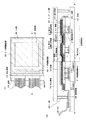
なお、図12(A)は、ボトムゲート型TFTを用いた発光装置の上面図である。ただし、封止基板による封止は、まだ行われていない。ソース側駆動回路1201、ゲート側駆動回路1202及び画素部1203が形成されている。また、図12(A)において、x−x’で発光装置を切ったときの画素部1203における領域a1204の断面図を図12(B)に示す。
【0128】
図12(B)では、画素部1203に形成されるTFTのうち電流制御用TFTについてのみ説明する。1211は基板であり、1212は下地となる絶縁膜(以下、下地膜という)である。基板1211としては透光性基板、代表的にはガラス基板、石英基板、ガラスセラミックス基板、又は結晶化ガラス基板を用いることができる。但し、作製プロセス中の最高処理温度に耐えるものでなくてはならない。
【0129】
また、下地膜1212は特に可動イオンを含む基板や導電性を有する基板を用いる場合に有効であるが、石英基板には設けなくても構わない。下地膜1212としては、珪素(シリコン)を含む絶縁膜を用いれば良い。なお、本明細書において「珪素を含む絶縁膜」とは、具体的には酸化珪素膜、窒化珪素膜若しくは窒化酸化珪素膜(SiOxNy:x、yは任意の整数、で示される)など珪素に対して酸素若しくは窒素を所定の割合で含ませた絶縁膜を指す。
【0130】
1213は電流制御用TFTであり、pチャネル型TFTで形成されている。なお、本実施例において、発光素子の陽極は電流制御用TFT1213と接続されているためpチャネル型TFTで形成されるのが望ましいが、これに限られることはなくnチャネル型TFTで形成しても良い。
【0131】
電流制御用TFT1213は、ソース領域1214、ドレイン領域1215及びチャネル形成領域1216を含む活性層と、ゲート絶縁膜1217と、ゲート電極1218と、層間絶縁膜1219と、ソース配線1220並びにドレイン配線1221を有して形成される。本実施例において電流制御用TFT1213はpチャネル型TFTである。
【0132】
また、スイッチング用TFTのドレイン領域は電流制御用TFT1213のゲート電極1218に接続されている。図示してはいないが、具体的には電流制御用TFT1213のゲート電極1218はスイッチング用TFTのドレイン領域(図示せず)とドレイン配線(図示せず)を介して電気的に接続されている。なお、ゲート電極1218はシングルゲート構造となっているが、マルチゲート構造であっても良い。また、電流制御用TFT1213のソース配線1220は電流供給線(図示せず)に接続される。
【0133】
電流制御用TFT1213は発光素子に注入される電流量を制御するための素子であり、比較的多くの電流が流れる。そのため、チャネル幅(W)はスイッチング用TFTのチャネル幅よりも大きく設計することが好ましい。また、電流制御用TFT1213に過剰な電流が流れないように、チャネル長(L)は長めに設計することが好ましい。望ましくは一画素あたり0.5〜2μA(好ましくは1〜1.5μA)となるようにする。
【0134】
また、電流制御用TFT1213の活性層(特にチャネル形成領域)の膜厚を厚くする(好ましくは50〜100nm、さらに好ましくは60〜80nm)ことによって、TFTの劣化を抑えてもよい。
【0135】
そして、電流制御用TFT1213の形成後、層間絶縁膜1219が形成され、電流制御用TFT1213と電気的に接続された陽極1223が形成される。なお、本実施例においては、電流制御用TFT1213と陽極1223を電気的に接続する配線及び陽極1223は同じ材料で同時に形成される。また、陽極1223を形成する材料としては、仕事関数がより大きい導電性材料を用いることが好ましい。その代表例として、ニッケル、パラジウム、タングステン、金、銀などの金属が挙げられる。なお、本実施例では、陽極1223は光を透過しないことが好ましいが、それに加えて、光の反射性の高い材料を用いることがさらに好ましい。
【0136】
陽極1223が形成された後に、絶縁層1224が形成される。なお、この絶縁層1224は、バンクともよばれる。
【0137】
つぎに有機化合物層が形成される。なお、本実施例における有機化合物層は、実施例1で説明したのと同じ構造を有する。すなわち高重合体からなる第1の有機化合物層1225、低重合体と蛍燐光体との共蒸着により形成される発光領域1226、及び低重合体からなる第2の有機化合物層1227で形成される。なお、これらの有機化合物層を形成する材料としては、実施例1に示したものを用いればよい。
【0138】
次に有機化合物層の上には、陰極1228が形成される。陰極1228の材料としては、仕事関数が2.5〜3.5eVの導電性材料を用いることが望ましい。代表的には、アルカリ金属元素もしくはアルカリ土類金属元素を含む導電膜、アルミニウムを含む導電膜、あるいはその導電膜にアルミニウムや銀などを積層したもの、を用いればよい。ただし、本実施例は上方出射であるため、陰極1228が光透過性であることが大前提である。したがって、これらの金属を用いる場合は、20nm程度の超薄膜であることが好ましい。
【0139】
以上により、逆スタガ型のTFTを有する発光装置を形成することができる。なお、本実施例により作製した発光装置は、図12(B)の矢印の方向(上面)に光を出射させることができる。
【0140】
逆スタガ型TFTは工程数がトップゲート型TFTよりも少なくし易い構造であるため、本発明の課題である製造コストの低減には非常に有利である。
【0141】
なお、本実施例の構成は、逆スタガ型TFTを有し、発光素子の陰極側から光を放出するという素子構造の発光装置について示したが、実施例4で示すトップゲート型TFTに本実施例で示した発光素子の陽極側から光を放出するという素子構造を組み合わせることも可能であり、また、本実施例の逆スタガ型TFTに実施例4で示す発光素子の陰極側から光を放出するという素子構造を組み合わせることも可能である。さらに、実施例1または実施例2に示した材料を自由に組み合わせて有機化合物層を形成することも可能である。
【0142】
(実施例7)
発光素子を用いた発光装置は自発光型であるため、液晶表示装置に比べ、明るい場所での視認性に優れ、視野角が広い。従って、様々な電気器具の表示部に用いることができる。
【0143】
本発明により作製した発光装置を用いた電気器具として、ビデオカメラ、デジタルカメラ、ゴーグル型ディスプレイ(ヘッドマウントディスプレイ)、ナビゲーションシステム、音響再生装置(カーオーディオ、オーディオコンポ等)、ノート型パーソナルコンピュータ、ゲーム機器、携帯情報端末(モバイルコンピュータ、携帯電話、携帯型ゲーム機または電子書籍等)、記録媒体を備えた画像再生装置(具体的にはデジタルビデオディスク(DVD)等の記録媒体を再生し、その画像を表示しうる表示装置を備えた装置)などが挙げられる。特に、斜め方向から画面を見る機会が多い携帯情報端末は、視野角の広さが重要視されるため、発光素子を有する発光装置を用いることが好ましい。それら電気器具の具体例を図10に示す。
【0144】
図10(A)は表示装置であり、筐体2001、支持台2002、表示部2003、スピーカー部2004、ビデオ入力端子2005等を含む。本発明により作製した発光装置は、表示部2003に用いることができる。発光素子を有する発光装置は自発光型であるためバックライトが必要なく、液晶表示装置よりも薄い表示部とすることができる。なお、表示装置は、パソコン用、TV放送受信用、広告表示用などの全ての情報表示用表示装置が含まれる。
【0145】
図10(B)はデジタルスチルカメラであり、本体2101、表示部2102、受像部2103、操作キー2104、外部接続ポート2105、シャッター2106等を含む。本発明により作製した発光装置は表示部2102に用いることができる。
【0146】
図10(C)はノート型パーソナルコンピュータであり、本体2201、筐体2202、表示部2203、キーボード2204、外部接続ポート2205、ポインティングマウス2206等を含む。本発明により作製した発光装置は表示部2203に用いることができる。
【0147】
図10(D)はモバイルコンピュータであり、本体2301、表示部2302、スイッチ2303、操作キー2304、赤外線ポート2305等を含む。本発明により作製した発光装置は表示部2302に用いることができる。
【0148】
図10(E)は記録媒体を備えた携帯型の画像再生装置(具体的にはDVD再生装置)であり、本体2401、筐体2402、表示部A2403、表示部B2404、記録媒体(DVD等)読み込み部2405、操作キー2406、スピーカー部2407等を含む。表示部A2403は主として画像情報を表示し、表示部B2404は主として文字情報を表示するが、本発明により作製した発光装置はこれら表示部A、B2403、2404に用いることができる。なお、記録媒体を備えた画像再生装置には家庭用ゲーム機器なども含まれる。
【0149】
図10(F)はゴーグル型ディスプレイ(ヘッドマウントディスプレイ)であり、本体2501、表示部2502、アーム部2503を含む。本発明により作製した発光装置は表示部2502に用いることができる。
【0150】
図10(G)はビデオカメラであり、本体2601、表示部2602、筐体2603、外部接続ポート2604、リモコン受信部2605、受像部2606、バッテリー2607、音声入力部2608、操作キー2609等を含む。本発明により作製した発光装置は表示部2602に用いることができる。
【0151】
ここで図10(H)は携帯電話であり、本体2701、筐体2702、表示部2703、音声入力部2704、音声出力部2705、操作キー2706、外部接続ポート2707、アンテナ2708等を含む。本発明により作製した発光装置は、表示部2703に用いることができる。なお、表示部2703は黒色の背景に白色の文字を表示することで携帯電話の消費電力を抑えることができる。
【0152】
なお、将来的に有機材料の発光輝度が高くなれば、出力した画像情報を含む光をレンズ等で拡大投影してフロント型若しくはリア型のプロジェクターに用いることも可能となる。
【0153】
また、上記電気器具はインターネットやCATV(ケーブルテレビ)などの電子通信回線を通じて配信された情報を表示することが多くなり、特に動画情報を表示する機会が増してきている。有機材料の応答速度は非常に高いため、発光装置は動画表示に好ましい。
【0154】
また、発光装置は発光している部分が電力を消費するため、発光部分が極力少なくなるように情報を表示することが好ましい。従って、携帯情報端末、特に携帯電話や音響再生装置のような文字情報を主とする表示部に発光装置を用いる場合には、非発光部分を背景として文字情報を発光部分で形成するように駆動することが好ましい。
【0155】
以上の様に、本発明の作製方法を用いて作製された発光装置の適用範囲は極めて広く、あらゆる分野の電気器具に用いることが可能である。また、本実施例の電気器具は実施例1〜実施例6を実施することにより作製された発光装置をその表示部に用いることができる。
【0156】
(実施例8)
通常、高分子系材料の溶解特性を利用した積層構造の形成は難しいとされているが、本実施例では、本発明における高重合体と低重合体に対する溶解性の異なる溶媒を見いだし、それぞれ別の溶媒に溶解させ、これをスピンコート法により積層形成する場合について示す。
【0157】
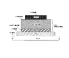
まず、陽極であるITOを100nm程度成膜したガラス基板上に、スピンコート法によりポリエチレンジオキシチオフェン/ポリスチレンスルホン酸(略称:PEDOT/PSS)の混合水溶液を塗布し、水分を蒸発させることで、正孔注入層を30nm成膜する。次に、高重合体である2,5−ジアルコキシ−ポリ(パラフェニレン)(略称:RO−PPP)(下記式(1))をトルエンに溶解し、スピンコート法で50nm成膜することで正孔輸送層を形成する。
【0158】
【式1】

次に、RO−PPPの低重合体(オリゴマー)であるRO−5P(下記式(2))およびドーパントであるルブレンをケトン系の溶媒(シクロヘキサノン等)に溶解し、発光領域として20nm程度成膜する。RO−PPPはケトン系の溶媒に対し溶解しにくいので、正孔輸送層と発光領域が混合してしまうことはない。なお、この時の発光領域は、層状ではなくクラスター状となっても良い。
【0160】
【式2】
なお、本実施例においては、上記に説明したスピンコート法のみで積層形成されたものを有機化合物層として用いることもできるが、この場合には、発光領域が、次に形成される陰極と接して形成される構造となるため、消光を招きやすい。そこで、本実施例において、さらに効率的に発光を得るためには発光領域と陰極との間に蒸着法により、電子輸送層を形成することが好ましい。なお電子輸送層を形成する材料としては、トリアゾール誘導体(TAZ)等を用いることができる。最後に陰極としてAl:Li合金を150nm蒸着し、本発明の発光素子が得られる。
【0162】
【発明の効果】
本発明を実施することにより、有機化合物層に高分子系材料を用いた発光装置において、その発光領域を所望の位置に設定することが可能となるため、発光素子における素子特性を向上させることができる。また、発光領域を陽極及び陰極から離した構造を形成することができるので、発光領域からのエネルギー移動による消光を防ぐことができる。
【図面の簡単な説明】
【図1】 本発明の発光装置の素子構造を説明する図。
【図2】 本発明の発光装置の作製工程を説明する図。
【図3】 蒸着室について説明する図。
【図4】 本発明の発光装置の素子構造を説明する図。
【図5】 本発明の発光装置の素子構造を説明する図。
【図6】 本発明の発光装置の素子構造を説明する図。
【図7】 発光装置の画素部の上面図。
【図8】 アクティブマトリクス型の発光装置を説明する図。
【図9】 パッシブマトリクス型の発光装置を説明する図。
【図10】 電気器具の一例を示す図。
【図11】 発光装置の従来例を説明する図。
【図12】 逆スタガ型TFTの構造を説明する図。[0001]
BACKGROUND OF THE INVENTION
The present invention relates to a light emitting device having a light emitting element using a polymer organic compound (polymer material). In particular, the present invention relates to a light-emitting device partially including a phosphor in an organic compound (polymer) composed of the same repeating unit, and a manufacturing method thereof. Note that the light-emitting device in this specification refers to an image display device, a light-emitting device, or a light source. Also, modules with light-emitting elements such as connectors such as FPC (Flexible printed circuit) or TAB (Tape Automated Bonding) tape or TCP (Tape Carrier Package), modules with a printed wiring board at the end of TAB tape or TCP Alternatively, all modules in which an IC (integrated circuit) is directly mounted on a light emitting element by a COG (Chip On Glass) method are included in the light emitting device.
[0002]
[Prior art]
The light emitting element as used in the field of this invention is an element light-emitted by applying an electric field. The light emission mechanism is such that when a voltage is applied with an organic compound layer sandwiched between electrodes, electrons injected from the cathode and holes injected from the anode recombine in the organic compound layer, and excited molecules (Hereinafter referred to as “molecular excitons”), and when the molecular excitons return to the ground state, they are said to emit energy and emit light.
[0003]
In addition, as a kind of molecular exciton which an organic compound forms, it is thought that a singlet excited state and a triplet excited state are possible, However, In this specification, the case where either excited state contributes to light emission is also included. I will do it.
[0004]
In such a light emitting device, the organic compound layer is usually formed as a thin film having a thickness of less than 1 μm. Further, since the light emitting element is a self-luminous element in which the organic compound layer itself emits light, a backlight as used in a conventional liquid crystal display is not necessary. Therefore, it is a great advantage that the light-emitting element can be manufactured to be extremely thin and light.
[0005]
For example, in an organic compound layer of about 100 to 200 nm, the time from carrier injection to recombination is about several tens of nanoseconds considering the carrier mobility of the organic compound layer. Even if the process from light emission to light emission is included, light emission occurs in the order of microseconds or less. Therefore, one of the features is that the response speed is very fast.
[0006]
Further, since the light-emitting element is a carrier injection type light-emitting element, it can be driven with a DC voltage, and noise is hardly generated. Regarding the driving voltage, the thickness of the organic compound layer is first made to be a uniform ultrathin film of about 100 nm, and electrode materials are selected so as to reduce the carrier injection barrier with respect to the organic compound layer, and further the heterostructure (two-layer structure). 100 cd / m at 5.5V 2 (Reference 1: CW Tang and SA Van Slyke, “Organic electroluminescent diodes”, Applied Physics Letters, vol. 51, No. 12, 913-915 (1987)).
[0007]
Due to these characteristics such as thin and light weight, high-speed response, and direct current low voltage drive, the light emitting element is attracting attention as a next-generation flat panel display element. Further, since it is a self-luminous type and has a wide viewing angle, the visibility is relatively good, and it is considered effective as an element used for a display screen of a portable device.
[0008]
By the way, as materials constituting the organic compound layer, there are two types of materials, low molecular weight materials and high molecular weight materials.
[0009]
Compared with the film formation surface, the low molecular weight material is formed as a thin film on the substrate by vacuum evaporation, whereas the high molecular weight material is formed on the substrate by a wet method such as spin coating from a solution of an organic solvent. It is different in that. In the case of forming a film by a vacuum deposition method, patterning using a conventional shadow mask technique is possible, and since it is a dry process in vacuum, there is an advantage that the purity of the material can be maintained. On the other hand, the spin coating method has the advantage that it is easy to form a film on a large area substrate and can be formed at a low cost in a short time, and development of devices utilizing the respective characteristics is being promoted. .
[0010]
However, from the viewpoint of materials, it is advantageous to use a polymer material having a physical property that the mechanical strength is high and aggregation and crystallization hardly occur. The fact that polymer materials are mechanically strong means that flexible elements that can be pulled and bent can be produced, and that aggregation and crystallization are unlikely to occur, and that they can be expected to be used under high temperature conditions. That's what it means. That is, by using a polymer material, the conditions for manufacturing the element are relaxed, and diversification of its application can be expected.
[0011]
In addition, in the organic compound layer, by forming a light emitting region containing a phosphor in a part of the organic compound layer, a carrier recombination region can be set to prevent carrier diffusion and the recombination region can be separated from the electrode. In addition, the emission characteristics were doubled (Reference 2: CW Tang, SA VanSlyke, and CHChen; Electro luminescence of doped organic thin films; J. Appl. Phys., Vol. 55, No. 9, 3510-3515. (1987)).
[0012]
In addition, in the organic compound layer of a light emitting element using a polymer material, a laminated structure as shown in FIG. 11 is well known, although it is different from forming a light emitting region by including a phosphor as a part thereof. Yes.
[0013]
In FIG. 11, an anode 1102, an
[0014]
[Problems to be solved by the invention]
However, the report that a carrier recombination region is set by forming a light emitting region containing a phosphor in a part of an organic compound layer is a case where a low molecular material is used, and a high molecular material is used. In such a case, there is a problem that it is difficult to form a light emitting region partially containing a phosphor because of its material characteristics.
[0015]
In the case of the laminated structure as shown in FIG. 11, functional separation is possible by a laminated structure using a polymer material. On the other hand, a material for forming the hole transport layer 1105 and the light emitting layer 1106 Therefore, there is a problem that quenching due to energy transfer tends to occur at the stack interface.
[0016]
Accordingly, in the present invention, in order to solve the above-described problems, in the manufacture of a light-emitting element having an organic compound layer using a polymer material, a phosphor is partially used without using a different polymer material for the organic compound layer. It is an object of the present invention to form a light-emitting element having excellent light-emitting characteristics by forming a region (light-emitting region) included in.
[0017]
In addition, by using such a light-emitting element, a light-emitting device having superior element characteristics than the conventional one is provided. Furthermore, the electric appliance produced using the said light-emitting device is provided.
[0018]
[Means for Solving the Problems]
The present invention is characterized in that a region containing a phosphor, that is, a light emitting region is formed in a part of an organic compound layer made of a polymer material. In the polymer material according to the present invention, a polymer having a polymerization degree of 2 to 5 formed of the same repeating units (which may have the same main chain structure) is called a low polymer, and the polymerization degree is low. More than 50 polymers are called high polymers.
[0019]
Conventionally, a polymer material is dissolved in a solvent to prepare a solution, and a film is formed by an ink jet method or a spin coat method. Therefore, it is impossible to form a light emitting region in a part of the organic compound layer, and there is a limit to the formation of a laminated structure using the dissolution characteristics of the polymer material.
[0020]
In the present invention, a solution in which a high polymer having a polymerization degree of 50 or more is dissolved in a solvent is formed by a spin coating method, and then the same polymer is composed of the same repeating unit. A light emitting region is formed by co-evaporating a certain low polymer and a phosphor, and only the low polymer is deposited on the light emitting region to form an organic compound layer. In the present invention, since both the high polymer and the low polymer are formed of the same repeating unit, the injection barrier at the laminated interface can be minimized.
[0021]
Furthermore, since the light emitting region formed in a part of the organic compound layer can be formed separately without being in contact with each of the anode and the cathode, quenching due to energy transfer to both electrodes can be prevented.
[0022]
The structure of the invention disclosed in this specification is a light-emitting device having a light-emitting element including an anode, an organic compound layer, and a cathode. The organic compound layer is formed of a polymer material, and is composed of a low polymer and phosphorescence. A light-emitting device including a light-emitting region including a body in a part thereof.
[0023]
According to another aspect of the present invention, there is provided a light emitting device having a light emitting element including an anode, an organic compound layer, and a cathode, wherein the organic compound layer is made of a polymer material having the same repeating unit and is phosphorescent. A light-emitting device including a light-emitting region including a body in a part thereof.
[0024]
According to another aspect of the invention, there is provided a light emitting device including a TFT provided on an insulating surface of a substrate, a light emitting element that is electrically connected to the TFT, and includes an anode, an organic compound layer, and a cathode. The compound layer is a light emitting device which is made of a polymer material and has a light emitting region including a low polymer and a phosphor in a part thereof.
[0025]
According to another aspect of the invention, there is provided a light emitting device including a TFT provided on an insulating surface of a substrate, a light emitting element that is electrically connected to the TFT, and includes an anode, an organic compound layer, and a cathode. The compound layer is a light emitting device which is made of a polymer material having the same repeating unit and has a light emitting region including a phosphor in a part thereof.
[0026]
In the light emitting device of the present invention, a low molecular material may be used for a part of the organic compound layer, and the structure of another invention includes a light emitting element including an anode, an organic compound layer, and a cathode. In the light emitting device, the organic compound layer is formed by being sandwiched between an anode and a cathode, and includes a first organic compound layer made of a high molecular weight material, and a second organic compound layer made of a low molecular weight material. Wherein the first organic compound layer has a light emitting region containing a low polymer and a phosphor as a part thereof, and the second organic compound layer is formed in contact with the cathode. It is a light-emitting device.
[0027]
According to another aspect of the present invention, there is provided a light emitting device having a light emitting element composed of an anode, an organic compound layer, and a cathode, wherein the organic compound layer is sandwiched between the anode and the cathode and is a polymer. A first organic compound layer made of a system material and a second organic compound layer made of a low molecular material, and the first organic compound layer is made of a polymer material having the same repeating unit. In addition, the light-emitting device includes a light-emitting region including a phosphor in part, and the second organic compound layer is formed in contact with the cathode.
[0028]
In each of the above structures, the polymer material is composed of the same repeating unit and a low polymer having a polymerization degree of 2 to 5 or a high polymer having a polymerization degree of 50 or more.
[0029]
In each of the above structures, the high molecular weight material is characterized by having N-vinylcarbazole or fluorene as a repeating unit.
[0030]
In each of the above structures, the phosphor is a substance that emits fluorescence or phosphorescence, and is 1,1,4,4-tetraphenyl-1,3-butadiene (hereinafter referred to as “TPB”), 4, 4′-bis (N- (1-naphthyl) -N-phenyl-amino) -biphenyl (hereinafter referred to as “α-NPD”), perylene, coumarin 6, 4-dicyanomethylene-2-methyl-6- ( p-dimethylamino-styryl) -4H-pyran (hereinafter referred to as “DCM1”), 4-dicyanomethylene-2-methyl-6- (julolidin-4-yl-vinyl) -4H-pyran (hereinafter referred to as “DCM2”). ), Rubrene, Nile red, N, N′-dimethyl-quinacridone (hereinafter referred to as dimethylquinacridone), anthracene, pyrene, 9,10-diphenylanthracene, tris ( 2-Phenylpyridine) iridium (hereinafter “Ir (ppy)” Three 1), 2,3,7,8,12,13,17,18-octaethyl-21H, 23H-porphyrin-platinum (hereinafter referred to as “PtOEP”). It is characterized by.
[0031]
In each of the above structures, the second organic compound layer is made of a low molecular material having an electron transporting property or a hole blocking property.
[0032]
In each of the above structures, the second organic compound layer includes an aluminum complex having a quinoline skeleton having an electron transport property, specifically, tris (8-quinolinolato) -aluminum (hereinafter referred to as “Alq”). Three ), Tris (4-methyl-8-quinolinolato) aluminum (hereinafter referred to as “Almq”), bis (2-methyl-8-quinolinolato)-(4-phenyl-phenolato) -aluminum (hereinafter referred to as “ A zinc complex having a benzoxazole skeleton or a benzothiazole skeleton, specifically bis (2- (2-hydroxyphenyl) -benzoxazolate) -zinc (hereinafter referred to as “Zn (PBO)”) 2 ), Bis (2- (2-hydroxyphenyl) -benzothiazolate) -zinc (hereinafter “Zn (PBT)”) 2 It is characterized by the following.
[0033]
In each of the above structures, the second organic compound layer is a 1,3,4-oxadiazole derivative (2- (4-biphenylyl) -5- (4- t-butylphenyl) -1,3,4-oxadiazole (hereinafter referred to as “PBD”), bathocuproin (hereinafter referred to as BCP), bathophenanthroline, or 1,2,4-triazole derivative 5- ( It is characterized by comprising 4-biphenylyl) -3- (4-tert-butylphenyl) -4-phenyl-1,2,4-triazole (hereinafter referred to as “TAZ”).
[0034]
In addition, the organic compound layer in each of the above structures is not formed using only the organic material described above, and may be formed by combining a known inorganic material with a part thereof. That is, the organic compound layer of the present invention includes those having an inorganic material as a part thereof.
[0035]
Conventionally, when a polymer material was used, the light emitting region could not be partially set. However, the organic compound layer made of a polymer material can be obtained by adopting the configuration of the present invention described above. In addition, since a light emitting region can be partially formed, quenching due to energy transfer can be prevented, so that element characteristics of the light emitting element can be improved.
[0036]
Note that light emission obtained from the light-emitting device of the present invention includes light emission from either a singlet excited state or a triplet excited state, or both.
[0037]
In addition, the structure related to the method for manufacturing the light-emitting device disclosed in this specification is that a high polymer is applied on the anode by a coating method to form a first organic compound layer, and then the first organic compound is formed by a co-evaporation method. A low polymer and a phosphor are vapor-deposited on the layer to form a light-emitting region, and a low polymer is vapor-deposited on the light-emitting region by a vapor deposition method to form a second organic compound layer. A method for manufacturing a light-emitting device, comprising forming an organic compound layer including a compound layer, a light-emitting region, and a second organic compound layer.
[0038]
In the production of the light emitting device of the present invention, a low molecular weight material may be used for a part of the organic compound layer, and the structure of another invention is that a high polymer is applied on the anode by a coating method. After forming an
[0039]
Note that in each of the above structures, the coating method is a spin coating method, a printing method, or an ink jet method.
[0040]
In each of the above structures, the high polymer has solubility in an organic solvent, and the low polymer and the low molecular weight material can be formed by an evaporation method.
[0041]
Further, in each of the above structures, a low polymer having a polymerization degree of 2 to 5 and a high polymer having a polymerization degree of 50 or more are used as the polymer material. This is a method for manufacturing a light emitting device.
[0042]
In each of the above structures, a material having a repeating unit of N-vinylcarbazole or fluorene is used as the polymer material.
[0043]
In each of the above-described structures, TPB, α-NPD, perylene, coumarin 6, DCM1, DCM2, rubrene, Nile red, dimethylquinacridone, anthracene, pyrene, 9,10-diphenylanthracene, Ir (ppy) are used as phosphors. Three , Using one or more selected from PtOEP.
[0044]
In each of the above structures, the organic solvent is toluene, benzene, chlorobenzene, dichlorobenzene, chloroform, tetralin, xylene, dichloromethane, cyclohexane, NMP (N-methyl-2-pyrrolidone), dimethyl sulfoxide, cyclohexanone, dioxane, THF. One or more selected from (tetrahydrofuran) are used.
[0045]
In each of the above structures, a material having an electron transporting property or a hole blocking property is used as the low molecular weight material.
[0046]
In the above structure, as a material having an electron transporting property, Alq Three , Almq, BAlq, Zn (PBO) 2 Or Zn (PBT) 2 It is characterized by using.
[0047]
In the above structure, PBD, BCP, bathophenanthroline, or TAZ is used as a material having a hole blocking property.
[0048]
DETAILED DESCRIPTION OF THE INVENTION
An embodiment of the present invention will be described with reference to FIGS. The light-emitting device of the present invention has a light-emitting element having the element structure shown in FIG.
[0049]
As shown in FIG. 1, an anode 102 is formed on a substrate 101, and an
[0050]
Further, a part of the
[0051]
Next, a method for manufacturing the light-emitting element illustrated in FIG. 1 will be described with reference to FIGS. As shown in FIG. 2A, an anode 202 is formed over a substrate 201. Note that in the present invention, light-transmitting glass or quartz is used for the substrate 201, and a light-transmitting conductive material is used for the anode 202.
[0052]
In addition, an insulating film made of an insulating material is formed on the anode 202. Note that the insulating layer 203 can be formed so as to cover an end portion of the anode 202 by partially etching the insulating film formed over the anode 202.
[0053]
Next, as illustrated in FIG. 2B, the first organic compound layer 204 is formed over the anode 202 and the insulating layer 203. In the present embodiment, the high molecular weight material forming the first organic compound layer 204 is preferably a material having a large work function and a hole transporting property, and a polymerization degree (n) of 50. The above high polymer is used.
[0054]
Here, a solution in which a high polymer is dissolved in an organic solvent is applied by a spin coating method, and this is further heated at 60 to 80 ° C. for 20 to 30 minutes to remove the organic solvent, whereby the first organic compound layer 204 is obtained. Note that the processing atmosphere at this time may be a vacuum.
[0055]
Then, a light emitting region 205 is formed over the first organic compound layer 204. In addition, in the formation of the light emitting region 205, a low polymer consisting of the same repeating unit as the high polymer used as the material of the first organic compound layer 204, the degree of polymerization (n) of 2 to 5, It is formed by co-evaporation of a phosphor that becomes the emission center.
[0056]
Note that when the light emitting region 205 is formed, film formation is performed in an evaporation chamber as shown in FIG. As shown in FIG. 3, the substrate 301 is fixed to a holder 302, and an evaporation source 303 (303 a and 303 b) is provided below the substrate 301. The evaporation source 303 (303a, 303b) includes an organic compound 304 (304a, 304b). In the present embodiment, the evaporation source 303a specifically includes a low polymer, The evaporation source 303b is provided with a phosphor. Further, a shutter 306 (306a, 306b) is formed in each of the evaporation sources 303 (303a, 303b). Note that the evaporation source 303 (303a and 303b) or the substrate 301 to be deposited is preferably moved (rotated) so that the film is uniformly formed in the film formation chamber 310.
[0057]
The evaporation source 303 (303a, 303b) is made of a conductive metal material. When the internal organic compound 304 (304a, 304b) is heated by resistance generated when a voltage is applied thereto, the evaporation source 303 (303a, 303b) is vaporized. Are deposited on the surface of the substrate 301. Note that in this specification, the surface of the substrate 301 includes a substrate and a thin film formed thereon, and here, an anode is formed on the substrate 301.
[0058]
The shutter 306 (306a, 306b) controls the vapor deposition of the vaporized organic compound 304 (304a, 304b). That is, when the shutter is open, the organic compound 304 (304a, 304b) vaporized by heating can be deposited.
[0059]
Further, the deposition chamber 310 is provided with an
[0060]
Note that the low polymer provided in the first evaporation source 303a and the phosphor provided in the second evaporation source 303b are simultaneously vapor-deposited (co-evaporated) on the substrate as shown in FIG. A light emitting region 205 is formed.
[0061]
Next, by closing only the
[0062]
Finally, the cathode 207 is formed on the second organic compound layer 206 using a conductive material, whereby the light emitting element 208 is formed.
[0063]
Through the above steps, a light-emitting element having the light-emitting region 105 in part of the
[0064]
In the present invention, a light emitting region 105 containing a phosphor is formed in a part of the
[0065]
Furthermore, in the present invention, not only the element structure shown in FIG. 1 but also a structure as shown in FIG. 4 can be formed. In FIG. 4, an
[0066]
In FIG. 4, a high polymer of a high molecular material is formed by spin coating, and a first
[0067]
Note that the second
[0068]
【Example】
(Example 1)
In this example, a light-emitting element having the structure described in FIG. 1 is described with reference to FIG.
[0069]
As shown in FIG. 5A, the element structure of the light-emitting element in this example is that an
[0070]
FIG. 5B shows details of the material structure for forming the
[0071]
In this embodiment, the high polymer 506 can be dissolved in an organic solvent, and the low polymer 507 is a sublimable material.
[0072]
Examples of the organic solvent for dissolving the high polymer in this example include toluene, benzene, chlorobenzene, dichlorobenzene, chloroform, tetralin, xylene, dichloromethane, cyclohexane, NMP (N-methyl-2-pyrrolidone), dimethyl sulfoxide, Cyclohexanone, dioxane, THF (tetrahydrofuran) and the like can be used.
[0073]
Further, as the phosphor 508 used in this embodiment, a fluorescent material and a phosphorescent material can be used.
[0074]
Examples of fluorescent materials include 1,1,4,4-tetraphenyl-1,3-butadiene (TPB), α-NPD, perylene, and coumarin 6 that can emit green light, and red (orange). In addition to DCM1, rubrene, and Nile red from which red light emission is obtained, dimethylquinacridone from which yellow-green light emission is obtained can be used. In addition, a fused polycyclic fluorescent material such as anthracene, pyrene, 9,10-diphenylanthracene, or the like can be used.
[0075]
In addition, as a phosphorescent material, Ir (ppy) which can obtain green light emission Three And red light emission PtOEP, a rare earth metal complex Eu (TTA) Three phen can be used. Ir (ppy) Three And DCM2 can be co-evaporated together to obtain red light emission.
[0076]
A method for manufacturing a light-emitting element in this example is described below. First, a film in which a polymer material is dissolved in an organic solvent is formed on the anode 501 by a spin coating method. Here, a solution in which a high polymer having N-vinylcarbazole as a repeating unit is used and dissolved in toluene is used. In this example, a high polymer having a fluorene compound as a repeating unit can also be used.
[0077]
When the film formation by the spin coating method is completed, this is further heated at 80 ° C. for 3 minutes to remove toluene, and a film made of the high polymer 506 is formed.
[0078]
Next, a low polymer 507 having a repeating unit of N-vinylcarbazole and a phosphor 508 are simultaneously co-evaporated to form a light emitting region 504.
[0079]
When the light emitting region 504 is formed, only a low polymer 507 (polymerization degree (n) = 2 to 5) of N-vinylcarbazole is formed by vapor deposition, and a film made of the low polymer 507 is formed. In addition, the film thickness formed at this time should just be 30-50 nm, and it forms with a film thickness of 40 nm in a present Example. Furthermore, in this example, the electron transport property can be enhanced by co-evaporating a low polymer of N-vinylcarbazole and PBD.
[0080]
Through the above steps, the
[0081]
Next, a cathode 503 is formed on the
[0082]
In addition, an ultrathin film insulating layer such as a metal oxide or a metal fluoride can be formed at the interface between the cathode 503 and the
[0083]
As described above, the light-emitting region 504 including the phosphor 508 at a desired position can be formed in the
[0084]
(Example 2)
In this embodiment, the case where the structure of the organic compound layer is different from that shown in
[0085]
As shown in FIG. 6A, the element structure of the light-emitting element in this example is that an
[0086]
FIG. 6B shows details of the material structure for forming the
[0087]
In this embodiment, the high polymer 608 can be dissolved in an organic solvent, and the low polymer 609 is a sublimable material.
[0088]
Furthermore, as an organic solvent for dissolving the high polymer in this example, toluene, benzene, chlorobenzene, dichlorobenzene, chloroform, tetralin, xylene, dichloromethane, cyclohexane, NMP (N-methyl-2-pyrrolidone), dimethyl sulfoxide, Cyclohexanone, dioxane, THF (tetrahydrofuran) and the like can be used.
[0089]
As the phosphor 610 used in this embodiment, a fluorescent material and a phosphorescent material similar to those shown in
[0090]
A method for manufacturing a light-emitting element in this example is described below. First, a film in which a polymer material is dissolved in an organic solvent is formed on the anode 601 by a spin coating method. Here, a solution in which a high polymer having N-vinylcarbazole as a repeating unit is used and dissolved in toluene is used. In this example, a high polymer having a fluorene compound as a repeating unit can also be used.
[0091]
When the film formation by the spin coating method is completed, this is further heated at 80 ° C. for 30 minutes to remove toluene, and a film made of the high polymer 608 is formed.
[0092]
Next, Ir (ppy) which is a low polymer 609 having a repeating unit of N-vinylcarbazole and a phosphor 610 Three Are co-evaporated to form a light emitting region 605.
[0093]
When the light emitting region 605 is formed, the electron transport layer 606 is formed by a vapor deposition method using the low molecular material 613. Note that the electron-transporting layer 606 formed here has a thickness of 30 to 50 nm.
[0094]
Note that the electron transport layer 606 formed in this embodiment includes a hole blocking layer. As an electron transporting organic compound forming the electron transport layer 606, Alq Three , Almq, BAlq, Zn (PBO) 2 Or Zn (PBT) 2 Further, as a hole blocking layer, a layer made of BCP, bathophenanthroline, PBD, TAZ may be sandwiched between the light emitting region and the electron transport layer.
[0095]
In this example, BCP and Alq Three Are stacked to form the electron transport layer 606 made of the low molecular material 613.
[0096]
As described above, the cathode 603 is formed when the
[0097]
Further, an alloy of aluminum and lithium (hereinafter referred to as Al: Li) or the like can be used.
[0098]
Further, an ultrathin film insulating layer such as a metal oxide or a metal fluoride can be formed at the interface between the cathode 603 and the
[0099]
As described above, in the
[0100]
(Example 3)
Here, FIG. 7A shows a detailed top structure of the pixel portion of the light-emitting device described in
[0101]
In this embodiment, the TFT shown in the
[0102]
The channel region of the switching
[0103]
The source of the
[0104]
Note that the configuration of this embodiment can be implemented by freely combining with the configuration of
[0105]
Example 4
In this embodiment, an external view of an active matrix light-emitting device manufactured by a manufacturing method of the present invention will be described with reference to FIGS. 8A is a top view illustrating the light-emitting device, and FIG. 8B is a cross-sectional view taken along line AA ′ in FIG. 8A. 801 indicated by a dotted line is a source side driver circuit, 802 is a pixel portion, and 803 is a gate side driver circuit. Reference numeral 804 denotes a sealing substrate, 805 denotes a sealing agent, and a space 807 is surrounded by the sealing
[0106]
Reference numeral 808 denotes a wiring for transmitting signals input to the source side driver circuit 801 and the gate side driver circuit 803, and receives a video signal and a clock signal from an FPC (flexible printed circuit) 809 serving as an external input terminal. Although only the
[0107]
Next, a cross-sectional structure is described with reference to FIG. A driver circuit and a pixel portion are formed over the substrate 810. Here, a source side driver circuit 801 and a pixel portion 802 are shown as driver circuits.
[0108]
Note that the source side driver circuit 801 is a CMOS circuit in which an n-
[0109]
The pixel portion 802 is formed by a plurality of pixels including a current control TFT 811 and an anode 812 electrically connected to the drain thereof.
[0110]
In addition, insulating
[0111]
The cathode 817 also functions as a wiring common to all pixels, and is electrically connected to the
[0112]
In addition, a sealing substrate 804 is attached with a
[0113]
Further, in this embodiment, a plastic substrate made of FRP (Fiberglass-Reinforced Plastics), PVF (polyvinyl fluoride), Mylar, polyester, acrylic, or the like is used as a material constituting the sealing substrate 804 as a material constituting the sealing substrate 804. be able to. In addition, after the sealing substrate 804 is bonded using the
[0114]
By encapsulating the light-emitting element in the space 807 as described above, the light-emitting element can be completely blocked from the outside, and a substance that promotes deterioration of the organic compound layer such as moisture and oxygen can be prevented from entering from the outside. Can do. Therefore, a highly reliable light-emitting device can be obtained.
[0115]
In addition, the structure of a present Example can be implemented in combination freely with any structure of Example 1-3.
[0116]
(Example 5)
In this embodiment, a case where a passive (simple matrix) light-emitting device having the element structure of the present invention is manufactured will be described. FIG. 9 is used for the description. In FIG. 9, 901 is a glass substrate and 902 is an anode made of a transparent conductive film. In this embodiment, a compound of indium oxide and zinc oxide is formed as a transparent conductive film by a vapor deposition method. Although not shown in FIG. 9, a plurality of anodes are arranged in stripes parallel to the paper surface.
[0117]
A
[0118]
Next, an
[0119]
Next, a low polymer of N-vinylcarbazole having a polymerization degree (n) of 2 to 5 and a phosphor that can be the emission center are co-evaporated to form a
[0120]
As the phosphor used in this embodiment, the same fluorescent material and phosphorescent material as those shown in
[0121]
Further, the second
[0122]
Next, the
[0123]
In this embodiment, since the lower electrode is formed of a light-transmitting
[0124]
Next, a ceramic substrate is prepared as the sealing
[0125]
The sealing
[0126]
(Example 6)
Although an active matrix light emitting device having a top gate TFT has been described in Embodiment 4, the present invention is not limited to the TFT structure, and therefore a bottom gate TFT (typically, as shown in FIG. 12). You may implement using a reverse stagger type TFT. Further, the reverse stagger type TFT may be formed by any means. Further, in Example 4, the structure obtained by emitting light obtained from the anode side (substrate side) light emitting element (downward emission type) is used. However, as shown in this example, the structure for emitting light from the cathode side (upper side) (Emission type).
[0127]
Note that FIG. 12A is a top view of a light-emitting device using a bottom-gate TFT. However, sealing with a sealing substrate has not been performed yet. A source side driver circuit 1201, a gate
[0128]
12B, only the current control TFT among TFTs formed in the pixel portion 1203 will be described. Reference numeral 1211 denotes a substrate, and
[0129]
In addition, the
[0130]
[0131]
The
[0132]
The drain region of the switching TFT is connected to the
[0133]
The
[0134]
Further, the deterioration of the TFT may be suppressed by increasing the thickness of the active layer (particularly the channel formation region) of the current control TFT 1213 (preferably 50 to 100 nm, more preferably 60 to 80 nm).
[0135]
After the
[0136]
After the
[0137]
Next, an organic compound layer is formed. The organic compound layer in this example has the same structure as that described in Example 1. That is, the first
[0138]
Next, a
[0139]
Through the above, a light-emitting device having an inverted staggered TFT can be formed. Note that the light-emitting device manufactured according to this example can emit light in the direction of the arrow (upper surface) in FIG.
[0140]
Since the inverted stagger type TFT has a structure in which the number of steps is easily reduced as compared with the top gate type TFT, it is very advantageous for reducing the manufacturing cost which is the subject of the present invention.
[0141]
Note that although the structure of this example shows a light emitting device having an element structure in which an inverted staggered TFT is provided and light is emitted from the cathode side of the light emitting element, this embodiment is applied to the top gate type TFT shown in Example 4. It is possible to combine the element structure of emitting light from the anode side of the light emitting element shown in the example, and emitting light from the cathode side of the light emitting element shown in Example 4 to the inverted staggered TFT of this example. It is also possible to combine the element structures of. Further, the organic compound layer can be formed by freely combining the materials shown in Example 1 or Example 2.
[0142]
(Example 7)
Since a light-emitting device using a light-emitting element is a self-luminous type, it is superior in visibility in a bright place and has a wide viewing angle as compared with a liquid crystal display device. Therefore, it can be used for display portions of various electric appliances.
[0143]
As an electric appliance using a light emitting device manufactured according to the present invention, a video camera, a digital camera, a goggle type display (head mounted display), a navigation system, a sound reproduction device (car audio, audio component, etc.), a notebook personal computer, a game A device, a portable information terminal (mobile computer, mobile phone, portable game machine, electronic book, etc.), an image playback device equipped with a recording medium (specifically, a recording medium such as a digital video disc (DVD)) And a device provided with a display device capable of displaying an image). In particular, a portable information terminal that frequently sees a screen from an oblique direction emphasizes the wide viewing angle, and thus a light emitting device having a light emitting element is preferably used. Specific examples of these electric appliances are shown in FIG.
[0144]
FIG. 10A illustrates a display device, which includes a
[0145]
FIG. 10B shows a digital still camera, which includes a
[0146]
FIG. 10C illustrates a laptop personal computer, which includes a
[0147]
FIG. 10D illustrates a mobile computer, which includes a
[0148]
FIG. 10E illustrates a portable image reproducing device (specifically, a DVD reproducing device) provided with a recording medium, which includes a
[0149]
FIG. 10F illustrates a goggle type display (head mounted display), which includes a
[0150]
FIG. 10G illustrates a video camera, which includes a main body 2601, a
[0151]
Here, FIG. 10H shows a mobile phone, which includes a
[0152]
If the emission luminance of the organic material is increased in the future, the light including the output image information can be enlarged and projected by a lens or the like and used for a front type or rear type projector.
[0153]
In addition, the electric appliances often display information distributed through electronic communication lines such as the Internet or CATV (cable television), and in particular, opportunities to display moving image information are increasing. Since the response speed of the organic material is very high, the light-emitting device is preferable for displaying moving images.
[0154]
In addition, since the light emitting portion of the light emitting device consumes power, it is preferable to display information so that the light emitting portion is minimized. Therefore, when a light emitting device is used for a display unit mainly including character information, such as a portable information terminal, particularly a mobile phone or a sound reproduction device, it is driven so that character information is formed by the light emitting part with the non-light emitting part as the background. It is preferable to do.
[0155]
As described above, the applicable range of the light-emitting device manufactured using the manufacturing method of the present invention is so wide that the light-emitting device can be used for electric appliances in various fields. Moreover, the electric appliance of a present Example can use the light-emitting device produced by implementing Example 1- Example 6 for the display part.
[0156]
(Example 8)
Usually, it is considered difficult to form a laminated structure using the solubility characteristics of a polymer material. However, in this example, a solvent having a different solubility in a high polymer and a low polymer in the present invention was found. In the case of forming a laminate by spin coating, this is dissolved.
[0157]
First, by applying a mixed aqueous solution of polyethylene dioxythiophene / polystyrene sulfonic acid (abbreviation: PEDOT / PSS) by spin coating on a glass substrate on which ITO serving as an anode is formed to a thickness of about 100 nm, A hole injection layer is formed to a thickness of 30 nm. Next, 2,5-dialkoxy-poly (paraphenylene) (abbreviation: RO-PPP) (the following formula (1)), which is a high polymer, is dissolved in toluene and formed into a film with a thickness of 50 nm by spin coating. A hole transport layer is formed.
[0158]
[Formula 1]
Next, RO-5P (the following formula (2)), which is a low polymer (oligomer) of RO-PPP, and rubrene, which is a dopant, are dissolved in a ketone-based solvent (cyclohexanone or the like) to form a film with a thickness of about 20 nm. To do. Since RO-PPP is difficult to dissolve in a ketone solvent, the hole transport layer and the light emitting region are not mixed. Note that the light emitting region at this time may be a cluster instead of a layer.
[0160]
[Formula 2]
In this embodiment, an organic compound layer formed only by the spin coating method described above can be used as the organic compound layer, but in this case, the light emitting region is in contact with the next formed cathode. As a result, the structure is easily extinguished. Therefore, in this embodiment, in order to obtain light emission more efficiently, it is preferable to form an electron transport layer between the light emitting region and the cathode by vapor deposition. As a material for forming the electron transport layer, a triazole derivative (TAZ) or the like can be used. Finally, an Al: Li alloy is deposited to a thickness of 150 nm as a cathode to obtain the light emitting device of the present invention.
[0162]
【The invention's effect】
By implementing the present invention, in a light emitting device using a polymer material for an organic compound layer, the light emitting region can be set at a desired position, so that the element characteristics of the light emitting element can be improved. it can. In addition, since a structure in which the light emitting region is separated from the anode and the cathode can be formed, quenching due to energy transfer from the light emitting region can be prevented.
[Brief description of the drawings]
1A and 1B illustrate an element structure of a light-emitting device of the present invention.
2A and 2B illustrate a manufacturing process of a light-emitting device of the present invention.
FIG. 3 illustrates a vapor deposition chamber.
4A and 4B illustrate an element structure of a light-emitting device of the present invention.
FIG. 5 illustrates an element structure of a light-emitting device of the present invention.
6A and 6B illustrate an element structure of a light-emitting device of the present invention.
FIG. 7 is a top view of a pixel portion of a light emitting device.
FIG. 8 illustrates an active matrix light-emitting device.
FIG 9 illustrates a passive matrix light-emitting device.
FIG. 10 is a diagram showing an example of an electric appliance.
FIG. 11 illustrates a conventional example of a light-emitting device.
FIG. 12 illustrates a structure of an inverted staggered TFT.
Claims (13)
前記発光素子を制御するためのTFTを有する発光装置において、 In a light emitting device having a TFT for controlling the light emitting element,
前記発光素子は、陽極と、有機化合物層と、陰極とを有し、 The light-emitting element has an anode, an organic compound layer, and a cathode,
前記有機化合物層は、前記陽極と前記陰極とに挟まれて形成され、第1の有機化合物層と、第2の有機化合物層とを有し、 The organic compound layer is formed between the anode and the cathode, and includes a first organic compound layer and a second organic compound layer,
前記第1の有機化合物層は、第1の重合体からなる層と、第2の重合体及び蛍燐光体からなる発光領域とを有し、 The first organic compound layer has a layer made of a first polymer, and a light emitting region made of a second polymer and a phosphor,
前記第1の重合体からなる層は、前記発光領域よりも陽極側に設けられ、 The layer made of the first polymer is provided on the anode side with respect to the light emitting region,
前記第2の有機化合物層は、前記第2の重合体からなり、前記陰極に接して形成され、 The second organic compound layer is made of the second polymer, is formed in contact with the cathode,
前記第1の重合体と前記第2の重合体とは主鎖の構造が同じであり、 The first polymer and the second polymer have the same main chain structure,
前記第1の重合体は、重合度が50以上であり、 The first polymer has a degree of polymerization of 50 or more,
前記第2の重合体は、第1の重合体よりも重合度が低く、蒸着法による成膜が可能である The second polymer has a lower degree of polymerization than the first polymer and can be deposited by vapor deposition.
ことを特徴とする発光装置。 A light emitting device characterized by that.
前記発光素子を制御するためのTFTを有する発光装置において、 In a light emitting device having a TFT for controlling the light emitting element,
前記発光素子は、陽極と、有機化合物層と、陰極とを有し、 The light-emitting element has an anode, an organic compound layer, and a cathode,
前記有機化合物層は、前記陽極と前記陰極とに挟まれて形成され、第1の有機化合物層と、第2の有機化合物層とを有し、 The organic compound layer is formed between the anode and the cathode, and includes a first organic compound layer and a second organic compound layer,
前記第1の有機化合物層は、第1の重合体からなる層と、第2の重合体及び蛍燐光体からなる発光領域とを有し、 The first organic compound layer has a layer made of a first polymer, and a light emitting region made of a second polymer and a phosphor,
前記第1の重合体からなる層は、前記発光領域よりも陽極側に設けられ、 The layer made of the first polymer is provided on the anode side with respect to the light emitting region,
前記第2の有機化合物層は、前記第2の重合体からなり、前記陰極に接して形成され、 The second organic compound layer is made of the second polymer, is formed in contact with the cathode,
前記第1の重合体と前記第2の重合体とは主鎖の構造が同じであり、 The first polymer and the second polymer have the same main chain structure,
前記第1の重合体は、重合度が50以上であり、 The first polymer has a degree of polymerization of 50 or more,
前記第2の重合体は、重合度が2〜5である The second polymer has a degree of polymerization of 2 to 5.
ことを特徴とする発光装置。 A light emitting device characterized by that.
前記発光素子を制御するためのTFTを有する発光装置において、 In a light emitting device having a TFT for controlling the light emitting element,
前記発光素子は、陽極と、有機化合物層と、陰極とを有し、 The light-emitting element has an anode, an organic compound layer, and a cathode,
前記有機化合物層は、前記陽極と前記陰極とに挟まれて形成され、第1の有機化合物層と、第2の有機化合物層とを有し、 The organic compound layer is formed between the anode and the cathode, and includes a first organic compound layer and a second organic compound layer,
前記第1の有機化合物層は、第1の重合体からなる層と、第2の重合体及び蛍燐光体からなる発光領域とを有し、 The first organic compound layer has a layer made of a first polymer, and a light emitting region made of a second polymer and a phosphor,
前記第1の重合体からなる層は、前記発光領域よりも陽極側に設けられ、 The layer made of the first polymer is provided on the anode side with respect to the light emitting region,
前記第2の有機化合物層は、電子輸送性または正孔阻止性を有する材料からなり、前記陰極に接して形成され、 The second organic compound layer is made of a material having an electron transport property or a hole blocking property, and is formed in contact with the cathode.
前記第1の重合体と前記第2の重合体とは主鎖の構造が同じであり、 The first polymer and the second polymer have the same main chain structure,
前記第1の重合体は、重合度が50以上であり、 The first polymer has a degree of polymerization of 50 or more,
前記第2の重合体は、前記第1の重合体よりも重合度が低く、 The second polymer has a lower degree of polymerization than the first polymer,
前記第2の重合体と、前記電子輸送性または正孔阻止性を有する材料とは、それぞれ、蒸着法による成膜が可能である The second polymer and the material having an electron transporting property or a hole blocking property can be formed by an evaporation method, respectively.
ことを特徴とする発光装置。 A light emitting device characterized by that.
前記発光素子を制御するためのTFTを有する発光装置において、 In a light emitting device having a TFT for controlling the light emitting element,
前記発光素子は、陽極と、有機化合物層と、陰極とを有し、 The light-emitting element has an anode, an organic compound layer, and a cathode,
前記有機化合物層は、前記陽極と前記陰極とに挟まれて形成され、第1の有機化合物層と、第2の有機化合物層とを有し、 The organic compound layer is formed between the anode and the cathode, and includes a first organic compound layer and a second organic compound layer,
前記第1の重合体からなる層は、前記発光領域よりも陽極側に設けられ、 The layer made of the first polymer is provided on the anode side with respect to the light emitting region,
前記第1の有機化合物層は、第1の重合体からなる層と、第2の重合体及び蛍燐光体からなる発光領域とを有し、 The first organic compound layer has a layer made of a first polymer, and a light emitting region made of a second polymer and a phosphor,
前記第2の有機化合物層は、電子輸送性または正孔阻止性を有する材料からなり、前記陰極に接して形成され、 The second organic compound layer is made of a material having an electron transport property or a hole blocking property, and is formed in contact with the cathode.
前記第1の重合体と前記第2の重合体とは主鎖の構造が同じであり、 The first polymer and the second polymer have the same main chain structure,
前記第1の重合体は、重合度が50以上であり、 The first polymer has a degree of polymerization of 50 or more,
前記第2の重合体は、重合度が2〜5であり、 The second polymer has a degree of polymerization of 2 to 5,
前記第2の重合体と、前記電子輸送性または正孔阻止性を有する材料とは、それぞれ、蒸着法による成膜が可能である The second polymer and the material having an electron transporting property or a hole blocking property can be formed by an evaporation method, respectively.
ことを特徴とする発光装置。 A light emitting device characterized by that.
層間絶縁膜を形成し、 Forming an interlayer insulation film,
前記TFTと電気的に接続された陽極を形成し、 Forming an anode electrically connected to the TFT;
前記陽極の上に、重合度が50以上である第1の重合体からなる層を塗布法によって形成し、 On the anode, a layer made of a first polymer having a polymerization degree of 50 or more is formed by a coating method,
前記第1の重合体からなる層の上に、前記第1の重合体と主鎖の構造が同じであり前記第1の重合体よりも重合度が低い第2の重合体と、蛍燐光体とからなる発光領域を蒸着法によって形成し、 A second polymer having a main chain structure identical to that of the first polymer and having a lower degree of polymerization than the first polymer, and a phosphor on the layer made of the first polymer; A light emitting region consisting of
前記発光領域の上に、前記第2の重合体からなる層を蒸着法によって形成し、 A layer made of the second polymer is formed on the light emitting region by vapor deposition,
前記第2の重合体からなる層の上に陰極を形成する Forming a cathode on the second polymer layer;
ことを特徴とする発光装置の作製方法。 A method for manufacturing a light-emitting device.
層間絶縁膜を形成し、 Forming an interlayer insulation film,
前記TFTと電気的に接続された陽極を形成し、 Forming an anode electrically connected to the TFT;
前記陽極の上に、重合度が50以上である第1の重合体からなる層を塗布法によって形成し、 On the anode, a layer made of a first polymer having a polymerization degree of 50 or more is formed by a coating method,
前記第1の重合体からなる層の上に、前記第1の重合体と主鎖の構造が同じであり重合度が2〜5である第2の重合体と、蛍燐光体とからなる発光領域を蒸着法によって形成し、 A light emission comprising a second polymer having the same main chain structure as that of the first polymer and a degree of polymerization of 2 to 5, and a phosphor on the first polymer layer. Forming the region by vapor deposition,
前記発光領域の上に、前記第2の重合体からなる層を蒸着法によって形成し、 A layer made of the second polymer is formed on the light emitting region by vapor deposition,
前記第2の重合体からなる層の上に陰極を形成する Forming a cathode on the second polymer layer;
ことを特徴とする発光装置の作製方法。 A method for manufacturing a light-emitting device.
層間絶縁膜を形成し、 Forming an interlayer insulation film,
前記TFTと電気的に接続された陽極を形成し、 Forming an anode electrically connected to the TFT;
前記陽極の上に、重合度が50以上である第1の重合体からなる層を塗布法によって形成し、 On the anode, a layer made of a first polymer having a polymerization degree of 50 or more is formed by a coating method,
前記第1の重合体からなる層の上に、前記第1の重合体と主鎖の構造が同じであり前記第1の重合体よりも重合度が低い第2の重合体と、蛍燐光体とからなる発光領域を蒸着法によって形成し、 A second polymer having a main chain structure identical to that of the first polymer and having a lower degree of polymerization than the first polymer, and a phosphor on the layer made of the first polymer; A light emitting region consisting of
前記発光領域の上に、電子輸送性または正孔阻止性を有する材料からなる層を蒸着法によって形成し、 A layer made of a material having an electron transport property or a hole blocking property is formed on the light emitting region by an evaporation method,
前記電子輸送性または正孔阻止性を有する材料からなる層の上に陰極を形成する A cathode is formed on the layer made of the electron transporting or hole blocking material.
ことを特徴とする発光装置の作製方法。 A method for manufacturing a light-emitting device.
層間絶縁膜を形成し、 Forming an interlayer insulation film,
前記TFTと電気的に接続された陽極を形成し、 Forming an anode electrically connected to the TFT;
前記陽極の上に、重合度が50以上である第1の重合体からなる層を塗布法によって形成し、 On the anode, a layer made of a first polymer having a polymerization degree of 50 or more is formed by a coating method,
前記第1の重合体からなる層の上に、前記第1の重合体と主鎖の構造が同じであり重合度が2〜5である第2の重合体と、蛍燐光体とからなる発光領域を蒸着法によって形成し、 A light emission comprising a second polymer having the same main chain structure as that of the first polymer and a degree of polymerization of 2 to 5, and a phosphor on the first polymer layer. Forming the region by vapor deposition,
前記発光領域の上に、電子輸送性または正孔阻止性を有する材料からなる層を蒸着法によって形成し、 A layer made of a material having an electron transport property or a hole blocking property is formed on the light emitting region by an evaporation method,
前記電子輸送性または正孔阻止性を有する材料からなる層の上に陰極を形成する A cathode is formed on the layer made of the electron transporting or hole blocking material.
ことを特徴とする発光装置の作製方法。 A method for manufacturing a light-emitting device.
Priority Applications (1)
| Application Number | Priority Date | Filing Date | Title |
|---|---|---|---|
| JP2002234079A JP4118630B2 (en) | 2001-07-13 | 2002-08-09 | LIGHT EMITTING DEVICE, ELECTRIC APPARATUS, AND METHOD FOR MANUFACTURING LIGHT EMITTING DEVICE |
Applications Claiming Priority (3)
| Application Number | Priority Date | Filing Date | Title |
|---|---|---|---|
| JP2001-213139 | 2001-07-13 | ||
| JP2001213139 | 2001-07-13 | ||
| JP2002234079A JP4118630B2 (en) | 2001-07-13 | 2002-08-09 | LIGHT EMITTING DEVICE, ELECTRIC APPARATUS, AND METHOD FOR MANUFACTURING LIGHT EMITTING DEVICE |
Related Parent Applications (1)
| Application Number | Title | Priority Date | Filing Date |
|---|---|---|---|
| JP2002200496A Division JP3766044B2 (en) | 2001-07-13 | 2002-07-09 | LIGHT EMITTING DEVICE, ITS MANUFACTURING METHOD, ELECTRIC APPARATUS |
Publications (3)
| Publication Number | Publication Date |
|---|---|
| JP2003092185A JP2003092185A (en) | 2003-03-28 |
| JP2003092185A5 JP2003092185A5 (en) | 2005-09-22 |
| JP4118630B2 true JP4118630B2 (en) | 2008-07-16 |
Family
ID=26618659
Family Applications (1)
| Application Number | Title | Priority Date | Filing Date |
|---|---|---|---|
| JP2002234079A Expired - Fee Related JP4118630B2 (en) | 2001-07-13 | 2002-08-09 | LIGHT EMITTING DEVICE, ELECTRIC APPARATUS, AND METHOD FOR MANUFACTURING LIGHT EMITTING DEVICE |
Country Status (1)
| Country | Link |
|---|---|
| JP (1) | JP4118630B2 (en) |
Cited By (1)
| Publication number | Priority date | Publication date | Assignee | Title |
|---|---|---|---|---|
| JP7142389B1 (en) | 2021-10-05 | 2022-09-27 | メイク株式会社 | capacitive level switch |
Families Citing this family (5)
| Publication number | Priority date | Publication date | Assignee | Title |
|---|---|---|---|---|
| JP5007544B2 (en) * | 2006-09-21 | 2012-08-22 | 大日本印刷株式会社 | SUBSTRATE FOR ORGANIC SEMICONDUCTOR DEVICE, SUBSTRATE WITH ORGANIC TRANSISTOR, AND ORGANIC SEMICONDUCTOR DEVICE USING THEM |
| SE534257C2 (en) | 2009-10-28 | 2011-06-21 | Lunavation Ab | A light emitting electrochemical device, a system comprising such a device and the use of such a device |
| US9142791B2 (en) | 2011-05-27 | 2015-09-22 | Universal Display Corporation | OLED having multi-component emissive layer |
| US9273079B2 (en) | 2011-06-29 | 2016-03-01 | Semiconductor Energy Laboratory Co., Ltd. | Organometallic complex, light-emitting element, light-emitting device, electronic device, and lighting device |
| JP6363836B2 (en) | 2012-12-20 | 2018-07-25 | 株式会社半導体エネルギー研究所 | Light emitting element |
Family Cites Families (3)
| Publication number | Priority date | Publication date | Assignee | Title |
|---|---|---|---|---|
| JPH0696858A (en) * | 1992-09-10 | 1994-04-08 | Toppan Printing Co Ltd | Organic thin film el element |
| JPH0860145A (en) * | 1994-08-25 | 1996-03-05 | Mitsubishi Chem Corp | Organic electroluminescent element |
| JP2001189193A (en) * | 1999-10-05 | 2001-07-10 | Matsushita Electric Ind Co Ltd | Light emission element and method of manufacturing the same, and display device and lighting device using the same |
-
2002
- 2002-08-09 JP JP2002234079A patent/JP4118630B2/en not_active Expired - Fee Related
Cited By (1)
| Publication number | Priority date | Publication date | Assignee | Title |
|---|---|---|---|---|
| JP7142389B1 (en) | 2021-10-05 | 2022-09-27 | メイク株式会社 | capacitive level switch |
Also Published As
| Publication number | Publication date |
|---|---|
| JP2003092185A (en) | 2003-03-28 |
Similar Documents
| Publication | Publication Date | Title |
|---|---|---|
| US7413916B2 (en) | Light-emitting device and manufacturing method thereof | |
| US7737630B2 (en) | Electroluminescence element and a light emitting device using the same | |
| US7548022B2 (en) | Electroluminescence device | |
| JP6049797B2 (en) | Method for manufacturing light emitting device | |
| JP4152665B2 (en) | Light emitting device and manufacturing method thereof | |
| US7220988B2 (en) | Luminescent device and process of manufacturing the same | |
| US7075228B2 (en) | Light emitting device and manufacturing method therefor | |
| JP4118630B2 (en) | LIGHT EMITTING DEVICE, ELECTRIC APPARATUS, AND METHOD FOR MANUFACTURING LIGHT EMITTING DEVICE | |
| JP3766044B2 (en) | LIGHT EMITTING DEVICE, ITS MANUFACTURING METHOD, ELECTRIC APPARATUS | |
| JP2003017276A (en) | Light-emitting device and its forming method | |
| JPWO2004068913A1 (en) | Light emitting device and manufacturing method thereof |
Legal Events
| Date | Code | Title | Description |
|---|---|---|---|
| A521 | Request for written amendment filed |
Free format text: JAPANESE INTERMEDIATE CODE: A523 Effective date: 20050420 |
|
| A621 | Written request for application examination |
Free format text: JAPANESE INTERMEDIATE CODE: A621 Effective date: 20050420 |
|
| TRDD | Decision of grant or rejection written | ||
| A01 | Written decision to grant a patent or to grant a registration (utility model) |
Free format text: JAPANESE INTERMEDIATE CODE: A01 Effective date: 20080422 |
|
| A61 | First payment of annual fees (during grant procedure) |
Free format text: JAPANESE INTERMEDIATE CODE: A61 Effective date: 20080423 |
|
| R150 | Certificate of patent or registration of utility model |
Free format text: JAPANESE INTERMEDIATE CODE: R150 |
|
| FPAY | Renewal fee payment (event date is renewal date of database) |
Free format text: PAYMENT UNTIL: 20110502 Year of fee payment: 3 |
|
| FPAY | Renewal fee payment (event date is renewal date of database) |
Free format text: PAYMENT UNTIL: 20110502 Year of fee payment: 3 |
|
| FPAY | Renewal fee payment (event date is renewal date of database) |
Free format text: PAYMENT UNTIL: 20110502 Year of fee payment: 3 |
|
| FPAY | Renewal fee payment (event date is renewal date of database) |
Free format text: PAYMENT UNTIL: 20120502 Year of fee payment: 4 |
|
| FPAY | Renewal fee payment (event date is renewal date of database) |
Free format text: PAYMENT UNTIL: 20120502 Year of fee payment: 4 |
|
| FPAY | Renewal fee payment (event date is renewal date of database) |
Free format text: PAYMENT UNTIL: 20130502 Year of fee payment: 5 |
|
| FPAY | Renewal fee payment (event date is renewal date of database) |
Free format text: PAYMENT UNTIL: 20130502 Year of fee payment: 5 |
|
| FPAY | Renewal fee payment (event date is renewal date of database) |
Free format text: PAYMENT UNTIL: 20140502 Year of fee payment: 6 |
|
| R250 | Receipt of annual fees |
Free format text: JAPANESE INTERMEDIATE CODE: R250 |
|
| R250 | Receipt of annual fees |
Free format text: JAPANESE INTERMEDIATE CODE: R250 |
|
| R250 | Receipt of annual fees |
Free format text: JAPANESE INTERMEDIATE CODE: R250 |
|
| R250 | Receipt of annual fees |
Free format text: JAPANESE INTERMEDIATE CODE: R250 |
|
| LAPS | Cancellation because of no payment of annual fees |