EP0855657A2 - System und Verfahren zur schnellen Fourier-Transformation - Google Patents
System und Verfahren zur schnellen Fourier-Transformation Download PDFInfo
- Publication number
- EP0855657A2 EP0855657A2 EP98100900A EP98100900A EP0855657A2 EP 0855657 A2 EP0855657 A2 EP 0855657A2 EP 98100900 A EP98100900 A EP 98100900A EP 98100900 A EP98100900 A EP 98100900A EP 0855657 A2 EP0855657 A2 EP 0855657A2
- Authority
- EP
- European Patent Office
- Prior art keywords
- ram
- data
- address
- symbol
- fast fourier
- Prior art date
- Legal status (The legal status is an assumption and is not a legal conclusion. Google has not performed a legal analysis and makes no representation as to the accuracy of the status listed.)
- Granted
Links
Images


Classifications
-
- G—PHYSICS
- G06—COMPUTING OR CALCULATING; COUNTING
- G06F—ELECTRIC DIGITAL DATA PROCESSING
- G06F17/00—Digital computing or data processing equipment or methods, specially adapted for specific functions
- G06F17/10—Complex mathematical operations
- G06F17/14—Fourier, Walsh or analogous domain transformations, e.g. Laplace, Hilbert, Karhunen-Loeve, transforms
- G06F17/141—Discrete Fourier transforms
Definitions
- the present invention relates to fast Fourier transforming apparatus and method for performing fast Fourier transform.
- OFDM orthogonal frequency division multiplex
- a variety of data can be efficiently transmitted within a limited frequency band by the OFDM, and the OFDM has a characteristic advantageous to the ground waves that it is excellent in avoiding multipath interference.
- the OFDM requires a large scale of fast Fourier transform of several thousand samples, and hence, decrease in cost of a fast Fourier transforming apparatus is significantly desired for practical use of the OFDM.
- This fast Fourier transforming apparatus includes three RAMs (random access memories) as a storage, one of which is an input buffer RAM for storing input data and the other two of which are fast Fourier transform RAMs for storing immediate data obtained during an operation and output data.
- RAMs random access memories
- input buffer RAM for storing input data
- fast Fourier transform RAMs for storing immediate data obtained during an operation and output data.
- This fast Fourier transforming apparatus includes, as a storage, pipeline registers at a predetermined number of stages disposed between operators, and each of the operators is pipeline-operated for the processing.
- this fast Fourier transforming apparatus is equivalent in the memory capacity to the aforementioned apparatus using the two RAMs, the apparatus using the pipeline registers has a problem that the orders of input data and output data are different from each other because data are output in the order of processing.
- the apparatus additionally includes a data arranging RAM so as to re-arrange the output data.
- the memory capacity of the apparatus using the pipeline registers is equivalent to that of the above-described fast Fourier transforming apparatus using the three RAMs.
- a fast Fourier transforming apparatus needs a storage for storing input data of one symbol, intermediate data obtained during the operation and output data. Furthermore, a fast Fourier transforming apparatus used for modulation-demodulation is required to process continuous plural symbols, and hence, it additionally needs another storage for storing input data of a following symbol in parallel with the processing of a current symbol. Since these storages occupy a larger part in the entire fast Fourier transforming apparatus, a cost of the fast Fourier transforming apparatus can be decreased by decreasing a necessary memory capacity.
- the two exemplified conventional fast Fourier transforming apparatuses are equivalent in their memory capacities.
- the fast Fourier transforming apparatus is realized by using ASICs or the like
- the former that can use a RAM library as a storage is advantageous in decreasing cost. Therefore, the configuration of the former apparatus is generally adopted in using ASICs or the like.
- the former apparatus requires the three RAMs each having a memory capacity sufficient for storing data of one symbol: one as the input buffer RAM and two as the fast Fourier transform RAMs.
- this fast Fourier transforming apparatus has a problem of a large circuit scale. This problem is more serious as the number of samples of every symbol is increased.
- the fast Fourier transform RAM can also be provided with the function as the input buffer RAM, so that the input buffer RAM can be omitted.
- the fast Fourier transform is performed as follows: First, input data is stored in the fast Fourier transform RAM, and a butterfly operation is performed with intermediate data stored in this fast Fourier transform RAM. Ultimately, the data stored in the fast Fourier transform RAM is read as output data.
- a necessary memory capacity required in fast Fourier transform is decreased, thereby decreasing a cost.
- the fast Fourier transforming apparatus of this invention for performing the fast Fourier transform comprises a RAM (random access memory) for storing input data of every symbol, one symbol corresponding to a unit of data for fast Fourier transform; and an FFT processor for performing a fast Fourier transform processing (FFT processing) using a butterfly operation on input data stored in the RAM, wherein the RAM stores data resulting from the FFT processing by the FFT processor on input data of one symbol stored in the RAM as output data of the one symbol, and the FFT processor performs the FFT processing in a manner that, among output data of one symbol and input data of another symbol to be stored in the RAM subsequently to the output data of the one symbol, data having a common index indicating orders thereof in the symbols are stored at the same address in the RAM.
- a RAM random access memory
- FFT processing fast Fourier transform processing
- the FFT processor includes a RAM address generator for generating an access address for the RAM, and makes an access to the RAM in accordance with an address generated by the RAM address generator, and the RAM address generator converts an address to be generated in every symbol, so that, among output data of one symbol and input data of another symbol to be stored in the RAM subsequently to the output data of the one symbol, data having a common index indicating orders thereof in the symbols are stored at the same address in the RAM.
- a RAM address generator for generating an access address for the RAM, and makes an access to the RAM in accordance with an address generated by the RAM address generator, and the RAM address generator converts an address to be generated in every symbol, so that, among output data of one symbol and input data of another symbol to be stored in the RAM subsequently to the output data of the one symbol, data having a common index indicating orders thereof in the symbols are stored at the same address in the RAM.
- the RAM address generator preferably converts an address to be generated in every symbol by using bit reverse in which bits of an address are grouped on the basis of a radix of the butterfly operation and an order of the bits is reversed by using each group as a unit.
- the FFT processor includes a butterfly operation unit for performing the FFT processing using the butterfly operation on input data stored in the RAM, and the butterfly operation unit is capable of performing plural sorts of FFT processings which use different butterfly operations but are substantially equivalent to one another, and changes the sort of FFT processing to be performed on every symbol so that, among output data of one symbol and input data of another symbol to be stored in the RAM subsequently to the output data of the one symbol, data having a common index indicating orders thereof in the symbols are stored at the same address in the RAM.
- the butterfly operation unit preferably alternately performs an FFT processing using a butterfly operation by decimation in frequency and an FFT processing using a butterfly operation by decimation in time on every symbol.
- the decimation in time and the decimation in frequency are equivalent to each other as the fast Fourier transform, but the order of the input data of one and the order of output data of the other are symmetrical. Therefore, by alternately adopting the decimation in time and the decimation in frequency, the data re-arrangement can be made unnecessary.
- the fast Fourier transforming apparatus of this invention for performing fast Fourier transform comprises first and second RAMs (random access memories) for storing input data of every symbol, one symbol corresponding to a unit of data for fast Fourier transform; and an FFT processor for performing a fast Fourier transform processing (FFT processing) using a butterfly operation on input data stored in the first or second RAM, wherein each of the first and second RAMs stores data resulting from the FFT processing by the FFT processor on input data of one symbol stored in the RAM as output data of the one symbol, one of the first and second RAMs is used for the FFT processing of even-numbered symbols and the other is used for the FFT processing of odd-numbered symbols, and the FFT processor performs the FFT processing in a manner that, among output data of an ith symbol (wherein i is a positive integer) and input data of an (i+2)th symbol, data having a common index indicating orders thereof in the symbols are stored at the same address in the first or second RAM.
- FFT processing fast Fourier transform processing
- the fast Fourier transforming method using a RAM of this invention comprises a first step of storing, in the RAM, pre-transform data of one symbol, one symbol corresponding to a unit of data for fast Fourier transform; a second step of performing a fast Fourier transform processing (FFT processing) using a butterfly operation on the pre-transform data stored in the RAM in the first step and storing resultant transformed data in the RAM; a third step of reading, from the RAM, the resultant transformed data stored in the RAM in the second step, wherein the first through third steps are repeatedly conducted, and an access address for the RAM is converted in every repeat, so that, among resultant transformed data stored in the RAM in an Nth repeat (wherein N is a positive integer) and pre-transform data stored in the RAM in an (N+1)th repeat, data having a common index indicating orders thereof in the symbols are stored at the same address of the RAM.
- FFT processing fast Fourier transform processing
- the fast Fourier transforming method using a RAM of this invention comprises a first step of storing, in the RAM, pre-transform data of one symbol, one symbol corresponding to a unit of data for fast Fourier transform; a second step of performing a fast Fourier transform processing (FFT processing) using a butterfly operation on the pre-transform data stored in the RAM in the first step and storing resultant transformed data in the RAM; and a third step of reading, from the RAM, the resultant transformed data stored in the RAM in the second step, wherein the first through third steps are repeatedly conducted, in the second step, plural sorts of FFT processings which use different butterfly operations but are substantially equivalent to one another are adoptable, and the sort of FFT processing to be performed is changed in every repeat, so that, among resultant transformed data stored in the RAM in an Nth repeat (wherein N is a positive integer) and pre-transform data stored in an (N+1)th repeat, data having a common index indicating orders thereof in the symbols are stored at the same address of the RAM.
- FFT processing fast
- variable bit reverse circuit of this invention which is included in the aforementioned fast Fourier transforming apparatus, for conducting bit reverse for a butterfly operation by a specified frequency, comprises serially connected plural bit reverse circuits each of which conducts one bit reverse, wherein, among the plural bit reverse circuits, bit reverse circuits in number corresponding to the specified frequency conduct the bit reverse and remaining bit reverse circuits allow data to pass therethrough.
- the OFDM receiver of this invention for demodulating a received OFDM signal into received data comprises a digital demodulation unit for demodulating an OFDM signal into a base band signal; and a fast Fourier transform unit for decoding complex data of carriers by performing fast Fourier transform on the base band signal obtained through demodulation by the digital demodulation unit, received data being generated on the basis of the complex data of the carriers, wherein the fast Fourier transform unit is composed of the aforementioned fast Fourier transforming apparatus.
- the OFDM transmitter of this invention for modulating data to be transmitted into an OFDM signal, comprises an inverse fast Fourier transform unit for performing inverse fast Fourier transform on complex data of carriers generated from data to be transmitted; and a digital modulation unit for generating an OFDM signal by frequency-converting output of the inverse fast Fourier transform unit, wherein the inverse fast Fourier transform unit is composed of an inverse fast Fourier transforming apparatus obtained by applying the above-described fast Fourier transforming apparatus.
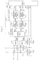
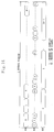
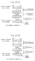
- Figure 1 is a block diagram for showing the configuration of the fast Fourier transforming apparatus of the first embodiment.
- reference numerals 101 and 102 denote first and second RAMs (which are shown as RAM#0 and RAM#1 in Figure 1) for storing input/output data and intermediate data obtained during a butterfly operation
- a reference numeral 103 denotes a butterfly operation unit for performing the butterfly operation
- a reference numeral 104 denotes a rotator generation unit for generating a rotator used in the butterfly operation
- a reference numeral 105 denotes a RAM address generator for generating addresses for accessing the first and second RAMs 101 and 102
- a reference numeral 106 denotes a control unit for controlling the RAM address generator 105 and the like.
- the RAM address generator 105 includes an input/output address generation unit 111 for generating an input/output dummy address DAD used as a RAM address reference in data input/output; a butterfly address generation unit 112 for generating a butterfly operation dummy address BAD used as a RAM address reference in the butterfly operation; a first variable bit reverse unit 113 for generating an input/output real address RDAD by conducting bit reverse (described in detail below) on the input/output dummy address DAD generated by the input/output address generation unit 111 by the number of times, that is, frequency specified in accordance with an input/output bit reverse signal DBR; a second variable bit reverse unit 114 for generating a butterfly operation real address RBAD by conducting the bit reverse on the butterfly operation dummy address BAD generated by the butterfly address generation unit 112 by a frequency specified in accordance with a butterfly operation bit reverse signal BBR; and an address selection unit 115 for receiving the input/output real address RDAD output by the first variable bit reverse unit 113
- a reference numeral 121 denotes a first data selection unit for receiving input data for the fast Fourier transforming apparatus and data resulting from the butterfly operation by the butterfly operation unit 103 and selectively outputting one of them as input data for the first RAM 101 and the other as input data for the second RAM 102
- a reference numeral 122 denotes a second data selection unit for receiving output data of the first and second RAMs 101 and 102 and selectively outputting one of them as output data of the fast Fourier transforming apparatus and the other as input data for the butterfly operation unit 103.
- the butterfly operation unit 103, the rotator generation unit 104, the RAM address generator 105, the control unit 106 and the first and second data selection units 121 and 122 together form an FFT processor.
- Figure 2 is a timing chart for showing a processing timing in the fast Fourier transforming apparatus of this embodiment.
- a processing of the ith symbol (wherein i is an integer)
- the butterfly operation is performed on the ith symbol during input of the (i+1)th symbol
- the symbol resulting from the Fourier transform is output during input of the (i+2)th symbol (which processing corresponds to hatched portions in Figure 2).
- the aforementioned operation of the fast Fourier transforming apparatus is realized by appropriately switching the two RAMs 101 and 102.
- Figure 3 is a timing chart for showing a RAM switching timing in the fast Fourier transforming apparatus of this embodiment.
- Figure 3 shows the RAM switching timing in performing the fast Fourier transform of N samples (wherein N is a positive integer), wherein x(0) through x(N-1) indicate input data (pre-transform data) in every symbol, and X(0) through X(N-1) indicate output data (post-transform data) in every symbol.
- an "FFT processing (i)" (wherein i is an integer) means the fast Fourier transform of an ith symbol.
- the symbol input (i) and symbol output (i-2) are performed in parallel in one symbol period by using the same RAM.
- the two RAMs 101 and 102 are alternately switched in respective symbol periods to be used as a symbol input/output RAM or a butterfly operation RAM.
- the two RAMs 101 and 102 are thus switched by the data selection units 121 and 122.
- one symbol period can be utilized as a period for the butterfly operation, which requires a large number of RAM accesses and calculations.
- the operation speed required of the first and second RAMs 101 and 102 can be decreased and the circuit scale of the butterfly operation unit 103 can be decreased.
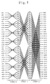
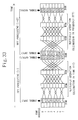
- Figure 4 is a signal flow graph for showing radix-4x2 decimation in time as an example of the fast Fourier transform algorithm
- Figure 5 is a diagram for showing operation elements in the signal flow graph.
- Figure 4 shows the signal flow graph adopted when the number N of samples is 32, wherein x(0) through x(N-1) indicate pre-transform input data, X(0) through X(N-1) indicate post-transform output data, and Wi indicates a coefficient of rotator multiplication.
- a "radix-4x2" operation means an operation combining a radix-4 butterfly operation and a radix-2 butterfly operation.
- the butterfly operation of several stages and the rotator multiplications between the stages are executed on the input data x(0) through x(N-1), thereby generating the output data X(0) through X(N-1).
- the radix-4x2 decimation in time shown in Figure 4 the radix-4 butterfly operation is performed in former two stages (i.e., a stage 0 and a stage 1), and the radix-2 butterfly operation is performed in the last stage (i.e., a stage 2).
- X0 x0 + x1 + x2 + x3
- X1 x0 - j ⁇ x1 - x2 + j ⁇ x3
- X2 x0 - x1 + x2 - x3
- X3 x0 + j ⁇ x1 - x2 - j ⁇ x3
- the fast Fourier transform algorithm has a characteristic that the orders of the input data x(0) through x(N-1) and the output data X(0) through X(N-1) are different from each other.
- the re-arrangement of the data is unnecessary because a processing equivalent to the data re-arrangement is realized by converting an address for accessing the RAM in every symbol by the bit reverse. Specifically, an address for accessing the RAM is converted in every symbol by changing the number of repeating times of the bit reverse on a reference address in every symbol (which is designated as variable bit reverse).
- Figures 6 and 7 are diagrams for showing an effect attained by the variable bit reverse of the addresses in this embodiment, wherein Figure 6 is a diagram for showing inter-RAM data transfer without the variable bit reverse of addresses and Figure 7 is a diagram for showing inter-RAM data transfer with the variable bit reverse of addresses.
- the number N of samples is 8, and the data transfer of merely one of the RAMs included in the fast Fourier transforming apparatus is shown.
- This RAM stores input/output data of even- or odd-numbered symbols and intermediate data obtained from the butterfly operation on the input data of these symbols.
- an output data X(k) of the FFT processing [i] and an input data x(k) of the FFT processing [i+2] are not necessarily stored at the same addresses of the RAM. Accordingly, the data are required to be re-arranged in order to store the input data x(k) of the FFT processing [i+2] in the same addresses from which the output data X(k) of the FFT processing [i] are read.
- an input/output address and a butterfly operation address are varied in each FFT processing by the bit reverse, so that the RAM address from which the output data X(k) of the FFT processing [i] is read can be the same as the RAM address at which the input data x(k) of the FFT processing [i+2] is stored. Accordingly, after reading the output data X(k) of the FFT processing [i], the input data x(k) of the FFT processing [i+2] can be stored at the same address. Thus, the input of a symbol and the output of another symbol preceding by two symbols can be overlapped.
- the variation of the input/output address and the butterfly operation address are controlled in accordance with the number of times, namely, frequency of the bit reverse.
- the bit reverse frequency is incremented in each FFT processing, and after attaining the maximum bit reverse frequency Rmax (wherein Rmax is a positive integer), it is initialized to be 0.
- the maximum bit reverse frequency Rmax can be obtained by subtracting one from a frequency required to return to an original address by repeating the bit reverse, and can be determined in accordance with the number of samples, the type of the butterfly operation used for the FFT processing and the like.
- the maximum bit reverse frequency Rmax is 2, and the bit reverse frequency is updated in each FFT processing so as to be repeatedly varied from 0 to 2.
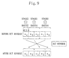
- Figure 8 is a diagram for showing the outline of the bit reverse.
- Figure 9 is a diagram for showing an example of the bit reverse, which is conducted in the radix-4x2 decimation in time on 32 samples as is shown in Figure 4.
- the binary is grouped successively from the LSB so that the groups can correspond to the respective stages of the butterfly operation. As is shown in Figure 4, the radix-4 butterfly operation is performed in the stages 0 and 1 and the radix-2 butterfly operation is performed in the stage 2.
- This embodiment adopts the variable bit reverse in which the bit reverse as is shown in Figures 8 and 9 is repeatedly conducted, so that the RAM addresses in the data input/output and the butterfly operation are appropriately converted.
- Figure 11 is a diagram for showing another example of the variation of an address by the variable bit reverse, shown correspondingly to inter-RAM data transfer adopted in the radix-4x2 decimation in time on 32 samples.
- the bit number of the address is 5.
- the 5 bits of the address are grouped successively from the LSB into a group of two bits, a group of two bits and a group of one bit, and the groups are reversed.
- a real address a4 a3 a2 a1 a0 (with the bit reverse frequency of 0), a real address a1 a0 a3 a2 a4 (with the bit reverse frequency of 1), a real address a2 a4 a0 a3 a1 (with the bit reverse frequency of 2), a real address a3 a1 a4 a0 a2 (with the bit reverse frequency of 3) and a real address a0 a2 a1 a4 a3 (with the bit reverse frequency of 4) can be generated through the bit reverse.
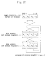
- Figure 12 is a diagram for showing still another example of the variation of an address by the variable bit reverse, shown correspondingly to inter-RAM data transfer conducted in the radix-4x2 decimation in time on 16 samples.
- the bit number of the address is 4.
- the 4 bits of the address are grouped successively from the LSB into a group of two bits and a group of two bits, and the groups are reversed.
- a real address a3 a2 a1 a0 (with the bit reverse frequency of 0) and a real address a1 a0 a3 a2 (with the bit reverse frequency of 1) can be generated through the bit reverse.
- the original address can always be attained by repeating the bit reverse of the address. Accordingly, the number of necessary real addresses is limited, and the real addresses can be generated by, for example, incrementing the bit reverse frequency on a reference address so as to be repeatedly varied from 0 to the maximum bit reverse frequency Rmax.
- the maximum bit reverse frequency Rmax is determined as follows: For example, in the case shown in Figure 10, the original address can be attained by repeating the bit reverse three times, and hence the maximum bit reverse frequency Rmax is 2. Similarly, in the case shown in Figure 11, the maximum bit reverse frequency Rmax is determined to be 4, and in the case shown in Figure 12, the maximum bit reverse frequency Rmax is determined to be 1. In the case where the radix-4x2 decimation in time is conducted by precedently using the radix-4 butterfly operation, the relationship between the number N of samples and the maximum bit reverse frequency Rmax can be represented as follows:
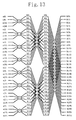
- Figure 13 is a signal flow graph adopted when the number N of samples is 32, for showing the processing order in the butterfly operation of this embodiment.
- the processing order in the butterfly operation is shown as numerals put on portions corresponding to the butterfly operation.
- the butterfly operation is performed on every 4s stages (wherein s is a stage number and is 0, 1, etc.) in the downward order in stages for the radix-4 operation, and is successively performed downward in stages for the radix-2 operation.
- Figures 14 and 15 are timing charts of signals generated by the control unit 106 for controlling the RAM address generator 105.
- DCN indicates an input/output timing signal for controlling the operation timing of the input/output address generation unit 111
- BCN and BST respectively indicate a butterfly operation timing signal and a butterfly operation stage signal for controlling the operation timing of the butterfly address generation unit 112.
- the butterfly operation stage signal BST has a value varying from 0 to (M-1) in one symbol period
- the butterfly operation timing signal BCN has a value varying from 0 to (N-1) in every period when the butterfly operation stage signal BST is constant.
- DBR indicates an input/output bit reverse signal for controlling the first variable bit reverse unit 113
- BBR indicates a butterfly operation bit reverse signal for controlling the second variable bit reverse unit 114
- RSL indicates a RAM selecting signal for controlling the selecting operation of the address selection unit 115.
- the butterfly operation bit reverse signal BBR is updated so as to be repeatedly changed from 0 to the maximum bit reverse frequency Rmax
- the input/output bit reverse signal DBR is updated so as to be repeatedly changed from 0 to the maximum bit reverse frequency Rmax with delayed from the butterfly operation bit reverse signal BBR by one symbol period.
- the RAM selecting signal RSL is switched between a "H" level and a "L" level in every symbol period.
- Figure 16 is a timing chart for showing the operating timing of the butterfly operation unit 103.
- the butterfly operation unit 103 performs three rotator multiplications and one radix-4 butterfly operation
- the butterfly operation unit 103 performs two rotator multiplications and two radix-2 butterfly operations.
- the butterfly operation unit 103 performs an operation with 4 inputs and 4 outputs.
- the butterfly operation unit 103 performs the rotator multiplication and the radix-4 or radix-2 butterfly operation on input data D0 through D3 read from the first or second RAM 101 or 102 through the second data selection unit 122, so as to output data X0 through X3.
- the data are input/output in each update cycle of the butterfly operation timing signal BCN generated by the control unit 106, and the output timing of the output data X0 through X3 is delayed from the input timing of the input data D0 through D3 by four cycles.
- the input/output address generation unit 111 receives the input/output timing signal DCN generated by the control unit 106 and generates the input/output dummy address DAD.
- the input/output dummy address DAD is determined regardless of the bit reverse frequency, and the input/output address generation unit 111 directly outputs the input/output timing signal DCN of 5 bits as the input/output dummy address DAD.
- the butterfly address generation unit 112 receives the butterfly operation timing signal BCN generated by the control unit 106 and generates the butterfly operation dummy address BAD.
- the butterfly operation dummy address BAD is determined regardless of the bit reverse frequency but on the basis of the number of stages and the radix of the butterfly operation.
- the butterfly address generation unit 112 generates the butterfly operation dummy address BAD in accordance with the butterfly operation stage signal BST by using a part of or all the bits of the butterfly operation timing signal BCN.
- the first variable bit reverse unit 113 receives the input/output dummy address DAD generated by the input/output address generation unit 111, and generates the input/output real address RDAD by conducting the bit reverse on the input/output dummy address DAD by a bit reverse frequency specified in accordance with the input/output bit reverse signal DBR generated by the control unit 106.
- the second variable bit reverse unit 114 receives the butterfly operation dummy address BAD generated by the butterfly address generation unit 112, and generates the butterfly operation real address RBAD by conducting the bit reverse on the butterfly operation dummy address BAD by a the bit reverse frequency specified in accordance with the butterfly operation bit reverse signal BBR generated by the control unit 106.
- Figures 17(a) and 17(b) are diagrams for showing examples of the configuration of the first and second variable bit reverse units 113 and 114.
- Figure 17(a) shows the configuration of a selector system.
- DAD input dummy address
- BAD bit reverse signal
- an address resulting from one bit reverse by a once bit reverse portion 501 an address resulting from two bit reverse by a twice bit reverse portion 502, etc.
- an address resulting from Rmax times of bit reverse by a Rmax times bit reverse portion 503 are respectively generated.
- a real address RDAD or RBAD
- DBR bit reverse signal
- Figure 17(b) shows the configuration of a table system.
- addresses resulting from the bit reverse of a dummy address DAD (or BAD) are previously stored in a table (ROM) 505.
- a real address RDAD (RBAD) is read from the table 505 by using, as a reference address, a data obtained by linking the bit reverse signal DBR (or BBR) to an upper (or a lower) position of the input dummy address DAD (or BAD) by a bit linking circuit 506.
- Figure 18 is a diagram for showing the input/output address generating operation by the input/output address generation unit 111 and the first variable bit reverse unit 113 of this embodiment, wherein correspondence of the input/output timing signal DCN and the input/output bit reverse signal DBR to the input/output dummy address DAD and the input/output real address RDAD is shown.
- the input/output dummy address DAD is always equal to the input/output timing signal DCN regardless of the input/output bit reverse signal DBR.
- the input/output real address RDAD is obtained by repeating the bit reverse by a frequency equal to the value of the input/output bit reverse signal DBR after grouping the input/output dummy address DAD from the LSB into a group of 2 bits, a group of 2 bits and a group of 1 bit.
- Figure 19 is a diagram for showing the butterfly operation address generating operation by the butterfly address generation unit 112 and the second variable bit reverse unit 114 of this embodiment, wherein correspondence of the butterfly operation timing signal BCN, the butterfly operation stage signal BST and the butterfly operation bit reverse signal BBR to the butterfly operation dummy address BAD and the butterfly operation real address RBAD is shown.
- the butterfly operation dummy address BAD is determined in accordance with the butterfly operation stage signal BST by using the butterfly operation timing signal BCN as a reference, regardless of the butterfly operation bit reverse signal BBR.
- the butterfly operation real address RBAD is obtained by repeating the bit reverse by a frequency equal to the value of the butterfly operation bit reverse signal BBR after grouping the butterfly operation real address BAD from the LSB into a group of 2 bits, a group of 2 bits and a group of 1 bit.
- the address selection unit 115 receives the input/output real address RDAD output by the first bit reverse unit 113 and the butterfly operation real address RBAD output by the second bit reverse unit 114, and selectively outputs one of them as the address for the first RAM 101 and the other as the address for the second RAM 102 in accordance with the RAM selecting signal RSL received from the control unit 106.
- Figure 20 is a diagram for showing the configuration of the address selection unit 115.
- reference numerals 601 through 603 denote selecting circuits
- reference numeral 611 through 614 denote registers.
- the other RAM receiving the butterfly operation real address RBAD from the address selection unit 115 data stored at the specified address RBAD is read as an input data for the butterfly operation unit 103 and output data of the butterfly operation unit 103 is then written at the same address.
- the address selection unit 115 includes, as is shown in Figure 20, the registers 611 through 614 for holding the butterfly operation address RBAD for a predetermined period of time.
- the registers 611 through 614 are operated synchronously with the update cycle of the butterfly operation timing signal BCN. Therefore, by using four stages of such serially connected registers, the butterfly operation real address RBAD can be held by the address selection unit 115 during the delay of the four cycles of the data output of the butterfly operation unit 113 from the data input thereof.
- the selecting circuit 603 selectively outputs either a butterfly operation real address RBAD or another butterfly operation real address RBAD delayed by four cycles in accordance with a butterfly operation address selecting signal BADSL.
- the selecting circuits 601 and 602 selectively output one of the input/output real address RDAD and the butterfly operation real address RBAD output by the selecting circuit 603 as the address for the first RAM 101 and the other as the address for the second RAM 102 in accordance with the RAM selecting signal RSL.
- Figures 21 and 22 are timing charts for showing the RAM access timing by using the RAM address output by the address selection unit 115, namely, the RAM address generated by the RAM address generator 105.
- Figure 21 shows the RAM access timing in the data input/output
- Figure 22 shows the RAM access timing in the butterfly operation.
- hatched portions correspond to a RAM access at the same address.
- one update cycle of the input/output timing signal DCN is halved, and the former half is used as a read cycle and the latter half is used as a write cycle of the RAM access.
- the data read and the data write in one update cycle of the input/output timing signal DCN are conducted at the same address.
- one update cycle of the butterfly operation timing signal BCN is halved as is shown in Figure 22, and the former half is used as a read cycle and the latter half is used as a write cycle of the RAM access.
- data read in one update cycle of the butterfly operation timing signal BCN and data write in another update cycle delayed by four cycles are conducted at the same address.
- an access address for the RAM is converted in every symbol by changing the frequency of the bit reverse conducted on a reference address in every symbol.
- data having a common index indicating their orders in the symbols can be stored at the same address of the RAM.
- input data of the following symbol can be written at the same address.
- a space area of the RAM from which the output data has been read can be used as an input buffer for storing the input data of the following symbol.
- the fast Fourier transforming apparatus can be realized by using two RAMs by appropriately switching the two RAMs so that the first RAM can be used for the processing of even-numbered symbols in continuous plural symbols and the second RAM can be used for the processing of odd-numbered symbols.
- variable bit reverse circuit which can generate addresses with regard to the respective sorts of numbers of samples by providing a variable bit reverse circuit having the configuration as is shown in Figure 17(a) with regard to each of the sorts of numbers of samples.
- the circuit scale is very large, resulting in disadvantageously increasing the entire circuit scale of the RAM address generator 105.
- variable bit reverse circuit which can realize plural types of variable bit reverse having different conversion patterns with a small circuit scale.
- Figure 23 is a diagram for showing another example of the configuration of the first and second variable bit reverse units 113 and 114, and is a circuit diagram of the variable bit reverse circuit which can realize plural types of variable bit reverse having different conversion patterns with a small circuit scale. Specifically, the variable bit reverse circuit of Figure 23 can execute the variable bit reverse on 4, 8, 16 and 32 samples.
- reference numerals 701 through 704 denote bit reverse circuits (BR)
- a reference numeral 711 denotes bit exchanging circuit (BC) as bit exchanging means
- a reference numeral 721 denotes a barrel shifter (BS) as bit shifting means.
- Figures 24(a) through 24(c) are circuit diagrams for showing the configurations of the respective circuits included in the variable bit reverse circuit of Figure 23, wherein Figure 24(a) shows the configuration of the bit reverse circuit BR, Figure 24(b) shows the configuration of the bit exchanging circuit BC and Figure 24(c) shows the configuration of the barrel shifter BS.
- bit reverse circuits 701 through 704 are controlled in accordance with respective bits of a bit reverse control signal BRSEL.
- BRSEL bit reverse control signal
- Figure 24(a) when the corresponding bit of the bit reverse control signal BRSEL is "0", each of the bit reverse circuits 701 through 704 allows the input data to pass therethrough, and when the corresponding bit is "1", each of the bit reverse circuits conducts the bit reverse by the radix-4x2 decimation in time on 32 samples as is shown in Figure 9.
- the operations are switched by a selector 801 in accordance with the bit reverse control signal BRSEL.
- bit exchanging circuit 711 is controlled in accordance with a bit exchange control signal BCSEL. As is shown in Figure 24(b), when the bit exchange control signal BCSEL is "0", the bit exchanging circuit 711 allows the input data to pass therethrough, and when the bit exchange control signal BSCEL is "1", the bit exchanging circuit 711 outputs data obtained by exchanging upper and lower bits of the input data. The operations are switched by a selector 802 in accordance with the bit exchange control signal BCSEL.
- the barrel shifter 721 is controlled in accordance with a shift control signal BSSEL (of 2 bits), and includes, as is shown in Figure 24(c), serial connection of a selector 803 controlled to be switched in accordance with the lower bit of the shift control signal BSSEL and a selector 804 controlled to be switched in accordance with the higher bit of the shift control signal BSSEL.
- BSSEL shift control signal
- the selector 803 allows the input data to pass therethrough, and when the lower bit is "1", the selector 803 shifts the input data rightward by 1 bit.
- the selector 804 When the upper bit of the shift control signal BSSEL is "0", the selector 804 allows the input data to pass therethrough, and when the higher bit is “1", the selector 804 shifts the input data rightward by 2 bits.
- the shift control signal BSSEL is "00" data input to the barrel shifter 721 is directly output as it is, when the shift control signal BSSEL is "01”, the input data is shifted rightward by 1 bit to be output, when the shift control signal BSSEL is "10”, the input data is shifted rightward by 2 bits to be output, and when the shift control signal BSSEL is "11", the input data is shifted rightward by 3 bits to be output.
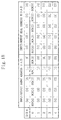
- Figures 25(a) through 25(d) are diagrams for showing set values of the respective control signals for the variable bit reverse circuit of Figure 23, wherein Figure 25(a) shows the values set when the number N of samples is 32, Figure 25(b) shows the values set when the number N of samples is 16, Figure 25(c) shows the values set when the number N of samples is 8, and Figure 25(d) shows the values set when the number N of samples is 4.
- the bit reverse control signal BRSEL is changed in accordance with the bit reverse frequency, and is set at such a value that, among the bit reverse circuits 701 through 704, merely those in number corresponding to the bit reverse frequency counted from the input port can conduct the bit reverse. For example, in the case where the number N of samples is 32, when the bit reverse frequency is 1, the bit reverse control signal BRSEL is set at "0001" so that the bit reverse circuit 701 alone can conduct the bit reverse, and when the bit reverse frequency is 3, the bit reverse control signal BRSEL is set at "0111" so that the bit reverse circuits 701 through 703 alone can conduct the bit reverse.
- the bit exchange control signal BSCEL is changed in accordance with the bit reverse frequency only when the number N of samples is 8, and is set at "1" only when the bit reverse circuit 701 conducts the bit reverse. Specifically, the bit exchanging circuit 711 conducts the bit exchange only when the number N of samples is 8 and the bit reverse frequency is 1 or 2. In cases apart from the case where the number N of samples is 32, the shift control signal BSSEL is set at a value except for "00" when the bit reverse frequency is odd. Also, the value of the shift control signal BSSEL is set in accordance with the number of samples.
- the shift control signal BSSEL is set at "01" as is shown in Figure 25(b), when the number N of samples is 8, it is set at "10” as is shown in Figure 25(c) and when the number N of samples is 4, it is set at "11” as is shown in Figure 25(d).
- the barrel shifter 721 shifts data rightward by 1 bit
- the number N of samples is 8 and the bit reverse frequency is 1
- the number N of samples is 4 and the bit reverse frequency is 1, it shifts data rightward by 3 bits.
- the variable bit reverse is conducted so that a real address a2 a1 a0 (with the bit reverse frequency of 0), a real address a1 a0 a2 (with the bit reverse frequency of 1) and a real address a0 a2 a1 (with the bit reverse frequency of 2) can be generated from a dummy address a2 a1 a0 before conducting the bit reverse.
- Figures 26(a) and 26(b) are diagrams for showing the operation of the variable bit reverse circuit of Figure 23 when the number N of samples is 8, wherein Figure 26(a) shows the operation with the bit reverse frequency of 1 and Figure 26(b) shows the operation with the bit reverse frequency of 2.
- bit reverse frequency 1
- bit exchange 1
- bit exchange is executed by the bit exchanging circuit 711
- bit reverse control signal BRSEL is "0001”
- the bit reverse is conducted by the bit reverse circuit 701 alone
- bit shift control signal BSSEL is "10”
- the two-bit shift is executed by the barrel shifter 721.
- the lower 3 bits of a bit string generated through this operation are used as an effective address, resulting in generating the real address a1 a0 a2 from the dummy address a2 a1 a0.
- bit reverse frequency 2
- bit exchange and two bit reverse are executed as is shown in Figure 26(b).
- bit exchange control signal BCSEL is "1”
- the bit exchange is executed by the bit exchanging circuit 711
- bit reverse control signal BRSEL is "0011”
- the bit reverse is executed by the bit reverse circuits 701 and 702.
- the bit shift control signal BSSEL is "00”
- the barrel shifter 721 does not execute the bit shift.
- the lower 3 bits of a bit string generated through this operation are used as an effective address, resulting in generating the real address a0 a2 a1 from the dummy address a2 a1 a0.
- FIGs 27(a) and 27(b) show the operation without the bit exchange, which results in malfunction as follows: When the bit reverse frequency is 1, an address a1 a0 a3 is generated as the real address as is shown in Figure 27(a), and when the bit reverse frequency is 2, an address a0 a3 a1 is generated as the real address as is shown in Figure 27(b).
- the bit reverse circuit BR is provided at stages in such a number that the variable bit reverse with the frequency corresponding to the number N(Mbr) of samples can be conducted.
- Mbr Mmax (when Mmax is odd)
- Mbr Mmax + 1 (when Mmax is even)
- bit exchanging circuits are inserted between every two stages of bit reverse circuits BR, counted from the input port.
- a barrel shifter with the maximum shift number of (Mmax - Mmin) is disposed subsequently to the bit reverse circuit BR at the last stage.
- bit reverse circuits BR those in number corresponding to the bit reverse frequency, counted from the input port, are operated.
- bit reverse frequency when the bit reverse frequency is not 0, merely the bit exchanging circuits BC disposed at bit positions AD[m] and AD[m-1] and closer to the input port than the operated bit reverse circuits BR are operated.
- the barrel shifter BS is operated for executing right shift by (Mmax - n) bits.
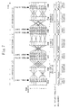
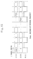
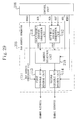
- Figure 29 is a block diagram for showing the configuration of a fast Fourier transforming apparatus of the second embodiment.
- a RAM address generator 205 and a control unit 206 are shown in Figure 29 because the fast Fourier transforming apparatus of this embodiment is different from the fast Fourier transforming apparatus of the first embodiment shown in Figure 1 in the inside configuration of the RAM address generator and a part of control signals.
- the RAM address generator 105 and the control unit 106 of Figure 1 are replaced with the RAM address generator 205 and the control unit 206 of Figure 29.
- the butterfly operation unit 103, the rotator generation unit 104, the RAM address generator 205, the control unit 206 and the first and second data selection units 121 and 122 together form an FFT processor.
- the RAM address generator 205 of this embodiment shown in Figure 29 is different from the RAM address generator 105 of the first embodiment shown in Figure 1 in an address selection unit 215 disposed at a stage preceding to the first and second variable bit reverse units 113 and 114.
- the input/output address generation unit 111 receives an input/output timing signal DCN, and generates and outputs an input/output dummy address DAD.
- the butterfly address generation unit 112 receives a butterfly operation timing signal BCN and a butterfly operation stage signal BST, and generates and outputs a butterfly operation dummy address BAD. These operations are the same as those of the first embodiment.
- the address selection unit 215 receives the input/output dummy address DAD output by the input/output address generation unit 111 and the butterfly operation dummy address BAD output by the butterfly address generation unit 112, and selectively outputs one of them as a dummy address for the first RAM 101 and the other as a dummy address for the second RAM 102 in accordance with a RAM selecting signal RSL.
- the first variable bit reverse unit 113 executes the bit reverse on the dummy address for the first RAM 101 output by the address selection unit 215 by a frequency specified in accordance with a first RAM bit reverse signal RBR0 output by the control unit 206, thereby outputting a real address for the first RAM 101.
- the second variable bit reverse unit 114 executes the bit reverse on the dummy address for the second RAM 102 output by the address selection unit 215 by a frequency specified in accordance with a second RAM bit reverse signal RBR1 output by the control unit 206, thereby outputting a real address for the second RAM 102.
- the RAM addresses can be determined substantially in the same manner as in the first embodiment.
- Figure 30 is a timing chart for showing the relationship between the first RAM bit reverse signal RBR0 and the second RAM bit reverse signal RBR1 generated by the control unit 206 and the operations of the first and second RAMs 101 and 102 (RAM#0 and RAM#1).
- the second RAM bit reverse signal RBR1 is updated to be repeatedly changed from 0 to Rmax
- the first RAM bit reverse signal RBR0 is updated to be repeatedly changed from 0 to Rmax with one symbol period delay from the second RAM bit reverse signal RBR1.
- the first and second RAMs 101 and 102 alternately repeat the data input/output and the butterfly operation.
- the fast Fourier transforming apparatus of this embodiment can realize the operation the same as that of the first embodiment and can attain the same effects as those of the first embodiment.
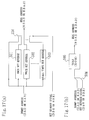
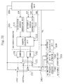
- FIG 31 is a block diagram for showing the configuration of a fast Fourier transforming apparatus of the third embodiment.
- a RAM address generator 305 of this embodiment does not include the variable bit reverse units but a butterfly operation unit 303 has a function to perform the butterfly operation not only by the decimation in time but also by decimation in frequency.
- the fast Fourier transform using the butterfly operation by the decimation in time and fast Fourier transform using the butterfly operation by the decimation in frequency are alternately executed on respective symbols.
- the decimation in time and the decimation in frequency are equivalent as the fast Fourier transform, but the order of input data of one and the order of output data of the other are symmetrical.
- the data rearrangement is made unnecessary by alternately adopting the decimation in time and the decimation in frequency.
- the butterfly operation unit 303 includes a decimation-in-frequency operator 341 for executing the butterfly operation by the decimation in frequency, a decimatin-in-time operator 342 for executing the butterfly operation by the decimation in time and a selecting circuit 343 for selectively outputting one of the results obtained by the decimation-in-frequency operator 341 and the decimation-in-time operator 342 in accordance with a thinning switching signal TSL supplied by a control unit 306.
- a reference numeral 304 denotes a rotator generation unit for generating a rotator used in the butterfly operation by the decimation in time or the decimation in frequency.
- a reference numeral 305 denotes the RAM address generator for generating addresses for controlling first and second RAMs 101 and 102.
- like reference numerals are used to refer to like elements used in Figure 1, and the description is herein omitted.
- the butterfly operation unit 303, the rotator generation unit 304, the RAM address generator 305, the control unit 306 and first and second data selection units 121 and 122 together form an FFT processor.
- one of the two RAMs 101 and 102 is used for the fast Fourier transform of even-numbered symbols and the other is used for the fast Fourier transform of odd-numbered symbols.
- a RAM address is converted in every symbol by the variable bit reverse in the first and second embodiments.
- the butterfly operation unit 303 is controlled so that the butterfly operation can be performed alternately by the decimation in time and by the decimation in frequency on respective symbols.
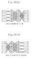
- Figures 32(a) and 32(b) are signal flow graphs for showing radix-2 decimation in time and radix-2 decimation in frequency on 8 samples, shown as examples of the fast Fourier transform algorithm, wherein Figure 32(a) shows the radix-2 decimation in time and Figure 32(b) shows the radix-2 decimation in frequency.
- Figure 32(a) shows the radix-2 decimation in time
- Figure 32(b) shows the radix-2 decimation in frequency.
- Figure 33 is a diagram for showing an example of inter-RAM data transfer in this embodiment, wherein the decimation in time and the decimation in frequency are alternately adopted on respective symbols.
- the number N of samples is 8, and the data transfer of merely one of the RAMs 101 and 102 is shown.
- the butterfly operation by the decimation in time is performed in an FFT processing [i] and the butterfly operation by the decimation in frequency is performed in an FFT processing [i+2].
- the order of the output data X(J) resulting from the butterfly operation by the decimation in time i.e., the FFT processing [i]
- the order of the input data x(j) in the butterfly operation by the decimation in frequency i.e., the FFT processing [i+2]).
- the order of the output data X(j) resulting from the butterfly operation by the decimation in frequency (i.e., the FFT processing [i+2]) accords with the order of the input data x(J) in the butterfly operation by the decimation in time (i.e., the FFT processing [i]).
- the order of the output data in each FFT processing accords with the order of the input data in a following FFT processing. Accordingly, a read address of output data X(k) in each FFT processing is the same as a write address of input data x(k) in a following FFT processing.
- the input data x(k) in the following FFT processing can be stored at the same address, and thus, the input of one symbol can be overlapped with the output of another symbol preceding by two symbols.
- the butterfly operation by the decimation in time and the butterfly operation by the decimation in frequency are alternately performed on respective symbols, so that, among output data of one symbol and input data of a following symbol, data having a common index indicating their orders in the symbols can be stored at the same address of the RAM.
- data having a common index indicating their orders in the symbols can be stored at the same address of the RAM.
- input data of the following symbol can be written at the same address of the RAM.
- a space area of the RAM from which the output data has been read can be used as the input buffer for storing the input data of the following symbol, and hence, there is no need to provide an input buffer RAM.
- the fast Fourier transforming apparatus using two RAMs can be realized by appropriately switching the two RAMs, so that the first RAM can be used for the processing of even-numbered symbols in continuous plural symbols and the second RAM can be used for the processing of odd-numbered symbols.
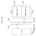
- Figure 34 is a diagram for showing the configuration of a fast Fourier transforming apparatus according to the fourth embodiment of the invention.
- a reference numeral 401 denotes a RAM for storing input/output data and intermediate data obtained in the butterfly operation
- a reference numeral 402 denotes a CPU for performing the butterfly operation and calculating an address for the RAM 401
- reference numerals 403 and 404 respectively denote an address bus and a data bus for connecting the RAM 401 and the CPU 402.
- the storage area of the RAM 401 is divided into two storage areas 405 and 406, one of which is used for the fast Fourier transform of even-numbered symbols and the other of which is used for the fast Fourier transform of odd-numbered symbols.
- the CPU 402 generates addresses for storing the input/output data and the intermediate data obtained in the butterfly operation in the two storage areas 405 and 406 of the RAM 401. Also, the CPU 402 performs the butterfly operation on input data read from the RAM 401 and outputs a result of the butterfly operation to the RAM 401.
- the storage area of the RAM is divided into the first and second storage areas, which are respectively used for the fast Fourier transform of even-numbered symbols and odd-numbered symbols in continuous plural symbols.
- the memory capacity of the RAM can be decreased.
- the two RAMs are provided for storing the input/output data and the intermediate data obtained in the butterfly operation, but these two RAMs can be replaced with two storage areas obtained by dividing one RAM as in this embodiment.
- decimation in time is adopted as the fast Fourier transform algorithm in the first and second embodiments, but the decimation in frequency can be adopted in stead.
- the operation by the butterfly operation unit is modified, and the grouping of address bits in the bit reverse by the variable bit reverse units is modified.
- the RAM address generator includes the two variable bit reverse units, but the RAM address generator can include merely one variable bit reverse unit and the bit reverse of the input/output address and the butterfly operation address can be conducted in a time sharing manner.
- the two RAMs are provided for storing the input/output data and the intermediate data obtained in the butterfly operation, but the number of RAMs used in this invention is not limited to two but can be one, or three or more.
- the present invention is also applicable to inverse fast Fourier transform similarly to the fast Fourier transform described in the respective embodiments.
- An inverse fast Fourier transform algorithm can be realized by partly changing the operation in the fast Fourier transform algorithm.
- radix-4x2 decimation in time as an example of the inverse fast Fourier transform algorithm can be expressed by a signal flow graph similar to that of the fast Fourier transform algorithm shown in Figure 4.
- the arithmetic expressions for operation elements are partly different from those of the fast Fourier transform algorithm.
- Figure 35 is a diagram for showing operation elements in assuming that the signal flow graph of Figure 4 shows the inverse fast Fourier transform algorithm.
- the operations as is shown in Figure 35 are conducted in accordance with the following arithmetic expressions, wherein difference from the arithmetic expressions for the operation elements in the fast Fourier transform shown in Figure 5 is underlined:
- X0 x0 + x1 + x2 + x3
- X1 x0 + j ⁇ x1 - x2 - j ⁇ x3
- X2 x0 - x1 + x2 - x3
- X3 x0 - j ⁇ x1 - x2 + j ⁇ x3
- the inverse fast Fourier transform of this invention can be realized by modifying the operations by the butterfly operation unit 103 and the rotator generation unit 104 in each of the first and second embodiments, by modifying the operations by the butterfly operation unit 303 and the rotator generation unit 304 in the third embodiment, and by modifying the butterfly operation and the rotator multiplication by the CPU 402 in the fourth embodiment.
- the butterfly operation unit 103, the rotator generation unit 104, the RAM address generator 105, the control unit 106 and the first and second data selection units 121 and 122 together form an IFFT processor for conducting the inverse fast Fourier transform using the butterfly operation.
- the fast Fourier transform apparatus of this invention can be used, for example, in an OFDM receiver.
- Figure 36 is a block diagram for showing the configuration of the OFDM receiver including the fast Fourier transforming apparatus of this invention, in which the fast Fourier transforming apparatus of this invention is used as a fast Fourier transform unit 12.
- a digital demodulation unit 11 converts an input OFDM signal into a base band signal through digital demodulation, and the fast Fourier transform unit 12 performs the fast Fourier transform on the base band signal output by the digital demodulation unit 11.
- An OFDM signal is a modulation signal using a large number of mutually orthogonal carriers, and complex data of respective carriers are decoded through the fast Fourier transform.
- the output of the fast Fourier transform unit 12 corresponds to decoded complex data of the carriers.
- An error correction/deinterleave/demapping unit 13 performs a predetermined error correction/deinterleave/demapping processing on the output of the fast Fourier transform unit 12, thereby decoding the received data.
- the inverse fast Fourier transforming apparatus of this invention can be used in, for example, an OFDM transmitter.
- Figure 37 is a block diagram for showing the OFDM transmitter including the inverse fast Fourier transforming apparatus of this invention, in which the inverse fast Fourier transforming apparatus of this invention is used as an inverse fast Fourier transform unit 22.
- a reverse processing to that in the OFDM receiver of Figure 36 is executed for generating an OFDM signal.
- a coding/interleave/mapping unit 21 conducts a predetermined error correction coding/interleave/mapping processing on data to be transmitted, thereby generating complex data of respective carriers.
- the inverse fast Fourier transform unit 22 performs the inverse fast Fourier transform on the complex data of the respective carriers, and a digital modulation unit 23 modulates the frequency of the output of the inverse fast Fourier transform unit 22.
- the OFDM signal is generated.
Landscapes
- Physics & Mathematics (AREA)
- Engineering & Computer Science (AREA)
- General Physics & Mathematics (AREA)
- Mathematical Physics (AREA)
- Computational Mathematics (AREA)
- Mathematical Analysis (AREA)
- Mathematical Optimization (AREA)
- Pure & Applied Mathematics (AREA)
- Data Mining & Analysis (AREA)
- Theoretical Computer Science (AREA)
- Discrete Mathematics (AREA)
- Algebra (AREA)
- Databases & Information Systems (AREA)
- Software Systems (AREA)
- General Engineering & Computer Science (AREA)
- Complex Calculations (AREA)
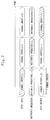
Applications Claiming Priority (6)
| Application Number | Priority Date | Filing Date | Title |
|---|---|---|---|
| JP920497 | 1997-01-22 | ||
| JP9204/97 | 1997-01-22 | ||
| JP920497 | 1997-01-22 | ||
| JP212861/97 | 1997-08-07 | ||
| JP21286197 | 1997-08-07 | ||
| JP21286197 | 1997-08-07 |
Publications (3)
| Publication Number | Publication Date |
|---|---|
| EP0855657A2 true EP0855657A2 (de) | 1998-07-29 |
| EP0855657A3 EP0855657A3 (de) | 1999-12-01 |
| EP0855657B1 EP0855657B1 (de) | 2007-03-14 |
Family
ID=26343892
Family Applications (1)
| Application Number | Title | Priority Date | Filing Date |
|---|---|---|---|
| EP98100900A Expired - Lifetime EP0855657B1 (de) | 1997-01-22 | 1998-01-20 | System und Verfahren zur schnellen Fourier-Transformation |
Country Status (5)
| Country | Link |
|---|---|
| US (2) | US6115728A (de) |
| EP (1) | EP0855657B1 (de) |
| CN (1) | CN1151454C (de) |
| CA (1) | CA2227677A1 (de) |
| DE (1) | DE69837299T2 (de) |
Cited By (4)
| Publication number | Priority date | Publication date | Assignee | Title |
|---|---|---|---|---|
| EP1058435A1 (de) * | 1999-06-02 | 2000-12-06 | STMicroelectronics SA | Verfahren und Einrichtung zur inversen Fouriertransformation in Pipeline-Architektur |
| WO2000049518A3 (de) * | 1999-02-18 | 2000-12-14 | Infineon Technologies Ag | Verfahren und vorrichtung zum berechnen einer diskreten orthogonalen transformation wie fft oder ifft |
| FR2794921A1 (fr) * | 1999-06-14 | 2000-12-15 | St Microelectronics Sa | Procede et dispositif de transformation de donnees reelles en symboles complexes, notamment pour la reception de porteuses modulees en phase et en amplitude et transmises sur une ligne telephonique |
| FR2916916A1 (fr) * | 2007-06-04 | 2008-12-05 | St Microelectronics Sa | Procede et dispositif electronique de decalage frequentiel d'un signal analogique, en particulier pour la telephonie mobile. |
Families Citing this family (49)
| Publication number | Priority date | Publication date | Assignee | Title |
|---|---|---|---|---|
| JPH11298436A (ja) * | 1998-02-13 | 1999-10-29 | Sony Corp | 変調方法、変調装置、復調方法及び復調装置 |
| US6351758B1 (en) * | 1998-02-13 | 2002-02-26 | Texas Instruments Incorporated | Bit and digit reversal methods |
| EP0942379A1 (de) * | 1998-03-13 | 1999-09-15 | Alcatel | Pipelineprozessor für die schnelle Fourier-Transformation |
| US6658441B1 (en) * | 1999-08-02 | 2003-12-02 | Seung Pil Kim | Apparatus and method for recursive parallel and pipelined fast fourier transform |
| US6643761B1 (en) * | 1999-09-08 | 2003-11-04 | Massana Research Limited | Address generation unit and digital signal processor (DSP) including a digital addressing unit for performing selected addressing operations |
| US7035892B2 (en) * | 1999-12-10 | 2006-04-25 | Broadcom Corporation | Apparatus and method for reducing precision of data |
| EP1162547A3 (de) * | 2000-06-05 | 2003-09-03 | DSP Group Ltd. | Von Ort FFTspeicherverwaltung |
| WO2002010994A1 (en) * | 2000-07-28 | 2002-02-07 | Delvalley Limited | A data processor |
| US6859816B2 (en) * | 2000-07-31 | 2005-02-22 | Sony Corporation | Fast Fourier transform method and inverse fast Fourier transform method |
| US7062523B1 (en) * | 2000-08-01 | 2006-06-13 | Analog Devices, Inc. | Method for efficiently computing a fast fourier transform |
| US6895421B1 (en) | 2000-10-06 | 2005-05-17 | Intel Corporation | Method and apparatus for effectively performing linear transformations |
| US20020156822A1 (en) * | 2001-01-10 | 2002-10-24 | Masaharu Tanai | High-speed FFT processing method and FFT processing system |
| KR100692997B1 (ko) * | 2001-04-17 | 2007-03-12 | 삼성전자주식회사 | 패스트퓨리에변환 장치 |
| JP4278317B2 (ja) * | 2001-07-05 | 2009-06-10 | 富士通マイクロエレクトロニクス株式会社 | 演算装置および受信装置 |
| WO2003021973A2 (en) * | 2001-09-01 | 2003-03-13 | Bermai, Inc. | Ram-based fast fourier transform unit for wireless communications |
| US20030126171A1 (en) * | 2001-12-13 | 2003-07-03 | Yan Hou | Temporal order independent numerical computations |
| US6963892B2 (en) * | 2001-12-26 | 2005-11-08 | Tropic Networks Inc. | Real-time method and apparatus for performing a large size fast fourier transform |
| US7047268B2 (en) * | 2002-03-15 | 2006-05-16 | Texas Instruments Incorporated | Address generators for mapping arrays in bit reversed order |
| US20040071199A1 (en) * | 2002-07-03 | 2004-04-15 | Commasic, Inc. | Virtual finger method and apparatus for processing digital communication signals |
| AU2002322795A1 (en) * | 2002-07-31 | 2004-02-23 | Thomson Licensing S.A. | Centralized buffer architecture for an orthogonal frequency division multiplexing (ofdm) receiver |
| GB2391966B (en) * | 2002-08-15 | 2005-08-31 | Zarlink Semiconductor Ltd | A method and system for performing a fast-fourier transform |
| EP1426872A3 (de) * | 2002-12-03 | 2006-02-22 | STMicroelectronics Ltd. | Linear skalierbare FFT/IFFT Berechnung in einem Multiprozessorsystem |
| TW594502B (en) * | 2003-01-30 | 2004-06-21 | Ind Tech Res Inst | Length-scalable fast Fourier transformation digital signal processing architecture |
| EP1447752A3 (de) * | 2003-02-17 | 2006-02-22 | STMicroelectronics Pvt. Ltd | Verfahren und System zur Mehrfachprozessor-FFT/IFFT-Berechnung mit minimaler Zwischenprozessorkommunikation |
| US20040172435A1 (en) * | 2003-02-27 | 2004-09-02 | Texas Instruments Incorporated | Architecture and method for performing a fast fourier transform and OFDM reciever employing the same |
| US7543010B2 (en) * | 2003-11-03 | 2009-06-02 | Board Of Regents, The University Of Texas System | Modular pipeline fast Fourier transform |
| US7529789B2 (en) * | 2004-11-01 | 2009-05-05 | Metanoia Technologies, Inc. | Method for representing complex numbers in a communication system |
| KR100602272B1 (ko) * | 2004-12-14 | 2006-07-19 | 삼성전자주식회사 | 고속으로 데이터를 처리하는 고속 퓨리에 변환 장치 및 방법 |
| US7577698B2 (en) * | 2004-12-28 | 2009-08-18 | Industrial Technology Research Institute | Fast fourier transform processor |
| JP2006331186A (ja) * | 2005-05-27 | 2006-12-07 | Ffc Ltd | Fft演算装置及びfft演算方法 |
| DE102005045519A1 (de) * | 2005-09-23 | 2007-03-29 | Newlogic Technologies Ag | Verfahren und Vorrichtung zur FFT Berechnung |
| US7817734B2 (en) * | 2005-10-18 | 2010-10-19 | Cisco Technology, Inc. | System and method for improving signal to quantization noise ratio of an OFDMA modulator |
| JP4698394B2 (ja) * | 2005-11-25 | 2011-06-08 | パナソニック株式会社 | 高速フーリエ変換回路 |
| WO2007127938A2 (en) * | 2006-04-28 | 2007-11-08 | Qualcomm Incorporated | Multi-port mixed-radix fft |
| ATE443896T1 (de) * | 2007-06-28 | 2009-10-15 | Ericsson Telefon Ab L M | Verfahren und vorrichtung zur transformationsberechnung |
| US8572147B2 (en) * | 2008-06-30 | 2013-10-29 | Freescale Semiconductor, Inc. | Method for implementing a bit-reversed increment in a data processing system |
| CN101354700B (zh) * | 2008-09-16 | 2010-08-11 | 四川虹微技术有限公司 | 一种蝶形运算fft处理器 |
| CN101504638B (zh) * | 2009-03-19 | 2010-12-01 | 北京理工大学 | 一种可变点数流水线fft处理器 |
| CN101847986B (zh) | 2009-03-27 | 2012-06-06 | 中兴通讯股份有限公司 | 一种实现fft/ifft变换的电路及方法 |
| KR101020295B1 (ko) * | 2009-03-30 | 2011-03-07 | 주식회사 하이닉스반도체 | 어드레스 변환회로 및 이를 이용한 반도체 메모리 장치 |
| CN101672873B (zh) * | 2009-10-20 | 2011-03-02 | 哈尔滨工业大学 | 一种基于Tsallis小波奇异熵与FFT运算结合的电力系统暂态谐波信号的检测方法 |
| US9846678B2 (en) | 2015-09-30 | 2017-12-19 | Apple Inc. | Fast Fourier Transform (FFT) custom address generator |
| US10257009B2 (en) | 2016-12-30 | 2019-04-09 | Waviot Integrated Systems, Llc | Method for multichannel signal search and demodulation and technique to demodulate and detect DBPSK FDMA ultra-narrow band signal |
| US10419063B2 (en) | 2016-12-30 | 2019-09-17 | Waviot Integrated Systems, Llc | Method and system for receiving telemetry messages over RF channel |
| US10326556B2 (en) | 2016-12-30 | 2019-06-18 | Waviot Integrated Systems, Llc | Method and system of frequency correction in LPWAN networks |
| US10291363B2 (en) | 2016-12-30 | 2019-05-14 | Waviot Integrated Systems, Llc | Method for simultaneous confirmation of many messages in low power wide area networks, and use of correction of frequency when transmitting data over UNB LPWAN networks, based on analysis of data obtained on receiving |
| CN115186223B (zh) * | 2022-07-25 | 2025-12-19 | 上海瑞浦青创新能源有限公司 | 一种傅里叶变换中位翻转置序列生成方法和装置 |
| CN120744293B (zh) * | 2025-09-04 | 2025-11-18 | 成都天奥信息科技有限公司 | 一种对序列依索引值按位倒序排序的电路及实现方法 |
| CN121412499A (zh) * | 2025-12-29 | 2026-01-27 | 中国计量大学 | 快速傅里叶变换的频谱提取方法及装置、计算机存储介质 |
Family Cites Families (22)
| Publication number | Priority date | Publication date | Assignee | Title |
|---|---|---|---|---|
| US3871577A (en) * | 1973-12-13 | 1975-03-18 | Westinghouse Electric Corp | Method and apparatus for addressing FFT processor |
| US4138730A (en) * | 1977-11-07 | 1979-02-06 | Communications Satellite Corporation | High speed FFT processor |
| JPS5482941A (en) * | 1977-12-15 | 1979-07-02 | Fujitsu Ltd | Fourier conversion processor |
| US4181976A (en) * | 1978-10-10 | 1980-01-01 | Raytheon Company | Bit reversing apparatus |
| US4689762A (en) | 1984-09-10 | 1987-08-25 | Sanders Associates, Inc. | Dynamically configurable fast Fourier transform butterfly circuit |
| JPS62175866A (ja) | 1986-01-30 | 1987-08-01 | Nec Corp | シグナルプロセツサ |
| USH570H (en) * | 1986-06-03 | 1989-01-03 | The United States Of America As Represented By The Secretary Of The Navy | Fast Fourier transform data address pre-scrambler circuit |
| US5012441A (en) * | 1986-11-24 | 1991-04-30 | Zoran Corporation | Apparatus for addressing memory with data word and data block reversal capability |
| JPS6432378A (en) * | 1987-07-29 | 1989-02-02 | Nec Corp | Bit inverting and transposing system |
| JPH01303565A (ja) * | 1988-05-31 | 1989-12-07 | Fujitsu Ltd | データ処理装置 |
| US5029079A (en) | 1988-08-04 | 1991-07-02 | Array Microsystems, Inc. | Apparatus and method for flexible control of digital signal processing devices |
| JPH02237374A (ja) * | 1989-03-10 | 1990-09-19 | Casio Comput Co Ltd | ディスクリートコサイン演算装置 |
| JP2958968B2 (ja) * | 1989-03-16 | 1999-10-06 | カシオ計算機株式会社 | ディスクリートコサイン演算装置 |
| JPH0431965A (ja) * | 1990-05-28 | 1992-02-04 | Nec Corp | 数値演算装置 |
| US5293330A (en) | 1991-11-08 | 1994-03-08 | Communications Satellite Corporation | Pipeline processor for mixed-size FFTs |
| JPH0668123A (ja) * | 1992-05-22 | 1994-03-11 | Nec Corp | 信号処理回路 |
| JPH0635951A (ja) * | 1992-07-16 | 1994-02-10 | Ricoh Co Ltd | 演算回路 |
| JP2851804B2 (ja) * | 1993-12-27 | 1999-01-27 | 松下電器産業株式会社 | 2次元直交変換装置 |
| US5583803A (en) | 1993-12-27 | 1996-12-10 | Matsushita Electric Industrial Co., Ltd. | Two-dimensional orthogonal transform processor |
| US5491652A (en) * | 1994-10-21 | 1996-02-13 | United Microelectronics Corporation | Fast Fourier transform address generator |
| JP3581193B2 (ja) * | 1995-06-29 | 2004-10-27 | 富士通テン株式会社 | マルチキャリア変調方式受信機 |
| JP3821316B2 (ja) * | 1996-08-06 | 2006-09-13 | ソニー株式会社 | 演算装置および方法 |
-
1998
- 1998-01-20 EP EP98100900A patent/EP0855657B1/de not_active Expired - Lifetime
- 1998-01-20 DE DE69837299T patent/DE69837299T2/de not_active Expired - Lifetime
- 1998-01-21 US US09/010,499 patent/US6115728A/en not_active Expired - Fee Related
- 1998-01-21 CA CA002227677A patent/CA2227677A1/en not_active Abandoned
- 1998-01-22 CN CNB981001572A patent/CN1151454C/zh not_active Expired - Fee Related
-
1999
- 1999-08-11 US US09/371,923 patent/US6247034B1/en not_active Expired - Lifetime
Cited By (9)
| Publication number | Priority date | Publication date | Assignee | Title |
|---|---|---|---|---|
| WO2000049518A3 (de) * | 1999-02-18 | 2000-12-14 | Infineon Technologies Ag | Verfahren und vorrichtung zum berechnen einer diskreten orthogonalen transformation wie fft oder ifft |
| EP1058435A1 (de) * | 1999-06-02 | 2000-12-06 | STMicroelectronics SA | Verfahren und Einrichtung zur inversen Fouriertransformation in Pipeline-Architektur |
| FR2794598A1 (fr) * | 1999-06-02 | 2000-12-08 | St Microelectronics Sa | Procede et dispositif de transformation de symboles complexes en des donnees reelles, notamment pour la transmission sur une ligne telephonique de porteuses modulees en phase et en amplitude |
| US6751642B1 (en) | 1999-06-02 | 2004-06-15 | Stmicroelectronics S.A. | Process and device for transforming complex symbols into real data, especially for the transmission over a telephone line of phase-modulated and amplitude-modulated carriers |
| FR2794921A1 (fr) * | 1999-06-14 | 2000-12-15 | St Microelectronics Sa | Procede et dispositif de transformation de donnees reelles en symboles complexes, notamment pour la reception de porteuses modulees en phase et en amplitude et transmises sur une ligne telephonique |
| EP1061704A1 (de) * | 1999-06-14 | 2000-12-20 | STMicroelectronics S.A. | Verfahren und Einrichtung zur schnellen Fouriertransformation zur OFDM-Demodulation |
| US6631167B1 (en) | 1999-06-14 | 2003-10-07 | Stmicroelectronics S.A. | Process and device for transforming real data into complex symbols, in particular for the reception of phase-modulated and amplitude-modulated carriers transmitted on a telephone line |
| FR2916916A1 (fr) * | 2007-06-04 | 2008-12-05 | St Microelectronics Sa | Procede et dispositif electronique de decalage frequentiel d'un signal analogique, en particulier pour la telephonie mobile. |
| WO2008152322A3 (fr) * | 2007-06-04 | 2009-05-22 | Centre Nat Rech Scient | Procede et dispositif electronique de decalage frequentiel d'un signal analogique, en particulier pour la telephonie mobile. |
Also Published As
| Publication number | Publication date |
|---|---|
| EP0855657A3 (de) | 1999-12-01 |
| DE69837299D1 (de) | 2007-04-26 |
| DE69837299T2 (de) | 2007-06-28 |
| CA2227677A1 (en) | 1998-07-22 |
| EP0855657B1 (de) | 2007-03-14 |
| CN1151454C (zh) | 2004-05-26 |
| US6247034B1 (en) | 2001-06-12 |
| US6115728A (en) | 2000-09-05 |
| CN1188939A (zh) | 1998-07-29 |
Similar Documents
| Publication | Publication Date | Title |
|---|---|---|
| US6115728A (en) | Fast fourier transforming apparatus and method, variable bit reverse circuit, inverse fast fourier transforming apparatus and method, and OFDM receiver and transmitter | |
| US7464127B2 (en) | Fast fourier transform apparatus | |
| US7164723B2 (en) | Modulation apparatus using mixed-radix fast fourier transform | |
| US6401162B1 (en) | Generalized fourier transform processing system | |
| KR100989797B1 (ko) | Fft/ifft 연산코어 | |
| US9727531B2 (en) | Fast fourier transform circuit, fast fourier transform processing method, and program recording medium | |
| JP3065979B2 (ja) | 高速フーリエ変換装置および方法、可変ビットリバース回路、逆高速フーリエ変換装置および方法、並びにofdm受信および送信装置 | |
| CN1965311A (zh) | 在就地计算中具有用于最小潜伏的分区存储的快速傅立叶变换电路 | |
| US6728742B1 (en) | Data storage patterns for fast fourier transforms | |
| US20060288068A1 (en) | Memory control method for storing operational result data with the data order changed for further operation | |
| EP1031933A2 (de) | Architektureffizienter digitaler Kanalformer mit diskreter Fourier-Transformation und Betriebsverfahren | |
| JPH08320858A (ja) | フーリエ変換演算装置および方法 | |
| US20060200513A1 (en) | Fast Fourier transform processor and method capable of reducing size of memories | |
| JPWO2011102291A1 (ja) | 高速フーリエ変換回路 | |
| US6789097B2 (en) | Real-time method for bit-reversal of large size arrays | |
| KR100557160B1 (ko) | 고속 퓨리에 변환을 이용한 혼합-기수 방식의 변조 장치 | |
| KR100484418B1 (ko) | 고속푸리에변환장치및방법,가변비트리버스회로,역고속푸리에변환장치및방법과직교주파수분할다중수신및송신장치 | |
| US6330287B1 (en) | Digital channelizer having efficient architecture for window presum using distributed arithmetic for providing window presum calculations in one clock cycle | |
| EP1032124A2 (de) | Architektureffizienter digitaler Kanalformer mit diskreter Fourier-Transformation von realen oder komplexen Daten und Betriebsverfahren | |
| CN116955899A (zh) | 一种信号处理方法及装置 | |
| KR20040046478A (ko) | 메모리의 크기를 감소시킬 수 있는 고속 퓨리에 변환프로세서 | |
| KR20060073426A (ko) | 직교 주파수 분할 다중화 시스템에서의 고속 푸리에 변환프로세서 및 그 변환 방법 | |
| CN120045513B (zh) | 一种基于粗粒度可重构架构的计算单元及fft处理器 | |
| JP5131346B2 (ja) | 無線通信装置 | |
| KR20250166678A (ko) | 고속 푸리에 변환 프로세서 |
Legal Events
| Date | Code | Title | Description |
|---|---|---|---|
| PUAI | Public reference made under article 153(3) epc to a published international application that has entered the european phase |
Free format text: ORIGINAL CODE: 0009012 |
|
| AK | Designated contracting states |
Kind code of ref document: A2 Designated state(s): DE FR GB NL |
|
| AX | Request for extension of the european patent |
Free format text: AL;LT;LV;MK;RO;SI |
|
| PUAL | Search report despatched |
Free format text: ORIGINAL CODE: 0009013 |
|
| AK | Designated contracting states |
Kind code of ref document: A3 Designated state(s): AT BE CH DE DK ES FI FR GB GR IE IT LI LU MC NL PT SE |
|
| AX | Request for extension of the european patent |
Free format text: AL;LT;LV;MK;RO;SI |
|
| 17P | Request for examination filed |
Effective date: 20000125 |
|
| AKX | Designation fees paid |
Free format text: DE FR GB NL |
|
| 17Q | First examination report despatched |
Effective date: 20040910 |
|
| GRAP | Despatch of communication of intention to grant a patent |
Free format text: ORIGINAL CODE: EPIDOSNIGR1 |
|
| GRAS | Grant fee paid |
Free format text: ORIGINAL CODE: EPIDOSNIGR3 |
|
| GRAA | (expected) grant |
Free format text: ORIGINAL CODE: 0009210 |
|
| AK | Designated contracting states |
Kind code of ref document: B1 Designated state(s): DE FR GB NL |
|
| PG25 | Lapsed in a contracting state [announced via postgrant information from national office to epo] |
Ref country code: NL Free format text: LAPSE BECAUSE OF FAILURE TO SUBMIT A TRANSLATION OF THE DESCRIPTION OR TO PAY THE FEE WITHIN THE PRESCRIBED TIME-LIMIT Effective date: 20070314 |
|
| REG | Reference to a national code |
Ref country code: GB Ref legal event code: FG4D |
|
| REF | Corresponds to: |
Ref document number: 69837299 Country of ref document: DE Date of ref document: 20070426 Kind code of ref document: P |
|
| ET | Fr: translation filed | ||
| NLV1 | Nl: lapsed or annulled due to failure to fulfill the requirements of art. 29p and 29m of the patents act | ||
| PLBE | No opposition filed within time limit |
Free format text: ORIGINAL CODE: 0009261 |
|
| STAA | Information on the status of an ep patent application or granted ep patent |
Free format text: STATUS: NO OPPOSITION FILED WITHIN TIME LIMIT |
|
| 26N | No opposition filed |
Effective date: 20071217 |
|
| PGFP | Annual fee paid to national office [announced via postgrant information from national office to epo] |
Ref country code: DE Payment date: 20110112 Year of fee payment: 14 |
|
| PGFP | Annual fee paid to national office [announced via postgrant information from national office to epo] |
Ref country code: GB Payment date: 20110119 Year of fee payment: 14 |
|
| PGFP | Annual fee paid to national office [announced via postgrant information from national office to epo] |
Ref country code: FR Payment date: 20120202 Year of fee payment: 15 |
|
| GBPC | Gb: european patent ceased through non-payment of renewal fee |
Effective date: 20120120 |
|
| PG25 | Lapsed in a contracting state [announced via postgrant information from national office to epo] |
Ref country code: DE Free format text: LAPSE BECAUSE OF NON-PAYMENT OF DUE FEES Effective date: 20120801 Ref country code: GB Free format text: LAPSE BECAUSE OF NON-PAYMENT OF DUE FEES Effective date: 20120120 |
|
| REG | Reference to a national code |
Ref country code: DE Ref legal event code: R119 Ref document number: 69837299 Country of ref document: DE Effective date: 20120801 |
|
| REG | Reference to a national code |
Ref country code: FR Ref legal event code: ST Effective date: 20130930 |
|
| PG25 | Lapsed in a contracting state [announced via postgrant information from national office to epo] |
Ref country code: FR Free format text: LAPSE BECAUSE OF NON-PAYMENT OF DUE FEES Effective date: 20130131 |