EP0848451A2 - Vorrichtung zum elektrischen und mechanischen Verbinden zweier im Abstand zueinander angeordneter Leiterplatten sowie Einrichtung mit zwei in Abstand zueinander angeordneten Leiterplatten, die durch eine derartige Vorrichtung verbunden sind - Google Patents
Vorrichtung zum elektrischen und mechanischen Verbinden zweier im Abstand zueinander angeordneter Leiterplatten sowie Einrichtung mit zwei in Abstand zueinander angeordneten Leiterplatten, die durch eine derartige Vorrichtung verbunden sind Download PDFInfo
- Publication number
- EP0848451A2 EP0848451A2 EP97120601A EP97120601A EP0848451A2 EP 0848451 A2 EP0848451 A2 EP 0848451A2 EP 97120601 A EP97120601 A EP 97120601A EP 97120601 A EP97120601 A EP 97120601A EP 0848451 A2 EP0848451 A2 EP 0848451A2
- Authority
- EP
- European Patent Office
- Prior art keywords
- insulating body
- soldering
- circuit board
- solder
- tongues
- Prior art date
- Legal status (The legal status is an assumption and is not a legal conclusion. Google has not performed a legal analysis and makes no representation as to the accuracy of the status listed.)
- Withdrawn
Links
Images


Classifications
-
- H—ELECTRICITY
- H05—ELECTRIC TECHNIQUES NOT OTHERWISE PROVIDED FOR
- H05K—PRINTED CIRCUITS; CASINGS OR CONSTRUCTIONAL DETAILS OF ELECTRIC APPARATUS; MANUFACTURE OF ASSEMBLAGES OF ELECTRICAL COMPONENTS
- H05K3/00—Apparatus or processes for manufacturing printed circuits
- H05K3/36—Assembling printed circuits with other printed circuits
- H05K3/368—Assembling printed circuits with other printed circuits parallel to each other
-
- H—ELECTRICITY
- H01—ELECTRIC ELEMENTS
- H01R—ELECTRICALLY-CONDUCTIVE CONNECTIONS; STRUCTURAL ASSOCIATIONS OF A PLURALITY OF MUTUALLY-INSULATED ELECTRICAL CONNECTING ELEMENTS; COUPLING DEVICES; CURRENT COLLECTORS
- H01R12/00—Structural associations of a plurality of mutually-insulated electrical connecting elements, specially adapted for printed circuits, e.g. printed circuit boards [PCB], flat or ribbon cables, or like generally planar structures, e.g. terminal strips, terminal blocks; Coupling devices specially adapted for printed circuits, flat or ribbon cables, or like generally planar structures; Terminals specially adapted for contact with, or insertion into, printed circuits, flat or ribbon cables, or like generally planar structures
- H01R12/50—Fixed connections
- H01R12/51—Fixed connections for rigid printed circuits or like structures
- H01R12/52—Fixed connections for rigid printed circuits or like structures connecting to other rigid printed circuits or like structures
-
- H—ELECTRICITY
- H05—ELECTRIC TECHNIQUES NOT OTHERWISE PROVIDED FOR
- H05K—PRINTED CIRCUITS; CASINGS OR CONSTRUCTIONAL DETAILS OF ELECTRIC APPARATUS; MANUFACTURE OF ASSEMBLAGES OF ELECTRICAL COMPONENTS
- H05K2201/00—Indexing scheme relating to printed circuits covered by H05K1/00
- H05K2201/10—Details of components or other objects attached to or integrated in a printed circuit board
- H05K2201/10227—Other objects, e.g. metallic pieces
- H05K2201/10424—Frame holders
-
- H—ELECTRICITY
- H05—ELECTRIC TECHNIQUES NOT OTHERWISE PROVIDED FOR
- H05K—PRINTED CIRCUITS; CASINGS OR CONSTRUCTIONAL DETAILS OF ELECTRIC APPARATUS; MANUFACTURE OF ASSEMBLAGES OF ELECTRICAL COMPONENTS
- H05K2201/00—Indexing scheme relating to printed circuits covered by H05K1/00
- H05K2201/10—Details of components or other objects attached to or integrated in a printed circuit board
- H05K2201/10613—Details of electrical connections of non-printed components, e.g. special leads
- H05K2201/10742—Details of leads
- H05K2201/1075—Shape details
- H05K2201/1084—Notched leads
-
- H—ELECTRICITY
- H05—ELECTRIC TECHNIQUES NOT OTHERWISE PROVIDED FOR
- H05K—PRINTED CIRCUITS; CASINGS OR CONSTRUCTIONAL DETAILS OF ELECTRIC APPARATUS; MANUFACTURE OF ASSEMBLAGES OF ELECTRICAL COMPONENTS
- H05K2203/00—Indexing scheme relating to apparatus or processes for manufacturing printed circuits covered by H05K3/00
- H05K2203/16—Inspection; Monitoring; Aligning
- H05K2203/167—Using mechanical means for positioning, alignment or registration, e.g. using rod-in-hole alignment
-
- H—ELECTRICITY
- H05—ELECTRIC TECHNIQUES NOT OTHERWISE PROVIDED FOR
- H05K—PRINTED CIRCUITS; CASINGS OR CONSTRUCTIONAL DETAILS OF ELECTRIC APPARATUS; MANUFACTURE OF ASSEMBLAGES OF ELECTRICAL COMPONENTS
- H05K3/00—Apparatus or processes for manufacturing printed circuits
- H05K3/30—Assembling printed circuits with electric components, e.g. with resistors
- H05K3/32—Assembling printed circuits with electric components, e.g. with resistors electrically connecting electric components or wires to printed circuits
- H05K3/34—Assembling printed circuits with electric components, e.g. with resistors electrically connecting electric components or wires to printed circuits by soldering
- H05K3/341—Surface mounted components
- H05K3/3421—Leaded components
- H05K3/3426—Leaded components characterised by the leads
-
- H—ELECTRICITY
- H05—ELECTRIC TECHNIQUES NOT OTHERWISE PROVIDED FOR
- H05K—PRINTED CIRCUITS; CASINGS OR CONSTRUCTIONAL DETAILS OF ELECTRIC APPARATUS; MANUFACTURE OF ASSEMBLAGES OF ELECTRICAL COMPONENTS
- H05K3/00—Apparatus or processes for manufacturing printed circuits
- H05K3/30—Assembling printed circuits with electric components, e.g. with resistors
- H05K3/32—Assembling printed circuits with electric components, e.g. with resistors electrically connecting electric components or wires to printed circuits
- H05K3/34—Assembling printed circuits with electric components, e.g. with resistors electrically connecting electric components or wires to printed circuits by soldering
- H05K3/3447—Lead-in-hole components
Definitions
- the invention relates to a device for electrical and mechanical Connecting two circuit boards arranged at a distance from one another, in particular a hybrid module with a basic carrier circuit board, the device connecting elements, each with a soldering pin has, and a device with two spaced apart Printed circuit boards connected by such a device are.
- connection combs made up of a number of individual contact elements that are like brackets embrace the side edges of a first circuit board and continue with their solder pins with a second circuit board e.g. through wave soldering are electrically and mechanically connected.
- the disadvantage here is that that the connection combs with a large number of electrical required Connections (e.g. larger than 40) the minimum size of the module plate specify so that all connections can be accommodated.
- the object of the invention is therefore a device for connection two printed circuit boards and a device with such a device specify which takes up less space and so the size of the circuit board does not depend on the number of connections required.
- solder tongues at the same time as others surface-mountable components can be attached and so on an additional soldering process, as is otherwise the case with the connection combs is necessary, can be dispensed with. Furthermore, the Use of the insulating body the mechanical stability of the connection increased and the ease of assembly further simplified, since to connect the two circuit boards, only a single component is required.
- the design of the insulating body as a frame Design achieved the space for a large number of fasteners offers and at the same time achieves mechanical stability, in particular if the frame is roughly the dimensions of the circuit board has, on which the tongues of the connecting elements are attached.
- the frame can be rectangular, square or even have an oval, round or polygonal shape.
- An arrangement of the soldering tongues such that they are under supervision of the frame are arranged outside the frame has the advantage that the Space on the first circuit board can be used optimally and thus also better unbundling of the circuit on the first circuit board is possible.
- the positioning aid is designed as an anti-rotation device, it is a reverse Assembly excluded.
- a locking lug is a simple permanent assembly the connecting elements in a previously produced insulating body, the receiving pockets for the locking lugs, possible. It is also possible to surround the connecting elements with the insulating body material and then bring it into the final form, e.g. by injection molding. However, this procedure is more complex overall.
- the elastic region such that between there is a narrow area between the soldering tongues and the intermediate area which is an angle of preferably 90 ° with the intermediate region includes, this is implemented in a manner that is easy to produce. Because the areas have different widths, the narrow area at give in to a load perpendicular to the soldering areas of the soldering tongues, like this e.g. due to bending due to the different Thermal expansion of the circuit boards connected by the device is caused.
- each an obtuse angle Due to the design of the narrow area of the connecting element with two opposite bends, each an obtuse angle include an easy to manufacture and permanent elasticity also realized parallel to the soldering surface of the soldering tongue.
- solder tabs By inserting a continuous opening in the solder tabs, that when placing the solder tabs on the with solder paste printed connection points not the solder paste to the side, but in the through opening is pressed and so good electrical and mechanical connection is guaranteed without the risk of that excess solder to short circuits with the adjacent solder joints leads.
- the connecting element as a tinned copper sheet stamped part is an inexpensive manufacture and assembly in the Insulating body possible.
- the device according to the invention it is possible to set up a device to be specified with two circuit boards arranged at a distance from one another, in which the device with a first circuit board by surface mounting is electrically and mechanically connected and in which the device with a second circuit board by push-through mounting electrically and is mechanically connected.
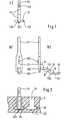
- FIG. 1 is the front view of a particularly preferred invention Connecting element 1 with a), the corresponding side view denoted by b) and the corresponding view from below c).
- the connecting element 1 is advantageously as a stamped and bent part made of tinned Executed copper sheet and has a solder pin 11, a narrow area 13 and a solder tongue 14. It is advantageous between the narrow area 13 and the solder pin 11 with an intermediate area 12 Latch 121 classified. The narrow area 13 closes with the intermediate area 12 an angle ⁇ of approximately 90 °.
- the necessary Bend 130 advantageously already has the width of the narrow area 13 on.
- the narrow area 13 also has two bends 131, 132, which include the obtuse angles ⁇ , ⁇ . If the angle ⁇ between the intermediate region 12 and the narrow region 13 90 ° is, the angles ⁇ , ⁇ are the same since the intermediate region 12 and the Soldering pin 11 advantageously perpendicular to the circuit boards to be connected stand.
- Figure 2 is a connecting element 1 of Figure 1 in a partial section a particularly preferred insulating body 2 shown.
- the insulating body 2 has a guide groove 21 and a receiving pocket 22.
- the guide groove 22 guides the connecting element 1 in the area of the intermediate area 12.
- the latch 121 is in the receiving pocket 22 locked and prevents the connecting element 1 from the Guide groove 21 can remove.
- the space 25 of the insulating body 2 is not necessary for the function of the device according to the invention, but simplifies the manufacture of the insulating body 2 and continues to save Material.
- Figure 3 shows the partial section of a device according to the invention between two circuit boards 3, 4 to be connected.
- the frame 20 also has Positioning aids 23, 24 on the corresponding recesses 32, 42 of the circuit boards 3, 4 engage and so the exact position of the frame 20 on the circuit boards 3, 4 determine.
- Positioning aids 23, 24 on the corresponding recesses 32, 42 of the circuit boards 3, 4 engage and so the exact position of the frame 20 on the circuit boards 3, 4 determine.
- the frame with the positioning aids 24 can then be placed on the top the circuit board 4 are placed and the solder pins 11 preferably in a wave soldering bath with the circuit board 4 electrically and mechanically be connected by means of the solder joints 41. You can do it at the same time the others by mounting on the top 43 of the circuit board 4 components to be assembled are soldered. Here too is a visual inspection of the solder joints 41 after the soldering is possible.
- the bends 130, 131, 132 described above make one such Elasticity ensures that the tongues 14 tear off from the solder joints 31 even when the circuit board 3 is bent due to the different Thermal expansion of the circuit boards 3, 4 is prevented.
- the insulating body designed as a frame 20 2, under which the soldering tongues 14 protrude into the interior of the frame 20. So the solder joints of the protruding solder tabs 14 are slightly optically too check.
- the frame has three positioning aids on its top 24 and on its underside two positioning aids 23. Through the illustrated Positioning the positioning aids is an accidental turning the printed circuit board 3.4 against each other.
- the frame 20 advantageously has approximately the same external dimensions as the first Circuit board 3, to which it is connected by surface mounting (reflow soldering) becomes. This makes it particularly stable and easy to install Connection of the circuit boards 3, 4 realized.
- a suitable one Material for the insulating body 2 in particular a plastic Above all, make sure that the insulating body has the required reflow soldering survives without deformation.
- soldering tongues 14 all outside the frame 20th show and the solder joints 31 on the first circuit board 3 also from can be checked optically above.
- This configuration is also equipping several printed circuit boards 3 in use with frame 20 and electronic components 5 and subsequent reflow soldering 34, 31 of all components 5, 20 to be mounted on the printed circuit board 3 possible and optimal use of the space on the first circuit board 3 possible.
- soldering tongues 14 it is also possible to use the soldering tongues 14 to be arranged both inside and outside a single frame 20.
Landscapes
- Engineering & Computer Science (AREA)
- Manufacturing & Machinery (AREA)
- Microelectronics & Electronic Packaging (AREA)
- Combinations Of Printed Boards (AREA)
- Coupling Device And Connection With Printed Circuit (AREA)
- Multi-Conductor Connections (AREA)
Abstract
Description
- Figur 1:
- Die Ansichten eines besonders bevorzugten Verbindungselements.
- Figur 2:
- Den Teilausschnitt durch einen besonders bevorzugten Isolierkörper mit einem eingesetzten Verbindungselement aus Figur 1.
- Figur 3:
- Den Teilschnitt einer besonders bevorzugten Vorrichtung zwischen zwei zu verbindenden Leiterplatten.
- Figur 4:
- Die Aufsicht auf eine bevorzugte Vorrichtung in Rahmenform.
- Figur 5:
- Die Aufsicht auf eine weitere bevorzugte Vorrichtung in Rahmenform, die auf eine erste Leiterplatte montiert ist.
Claims (17)
- Vorrichtung zur elektrischen und mechanischen Verbindung zweier im Abstand zueinander angeordneter Leiterplatten (3, 4), insbesondere eines Hybridmoduls mit einer Grundträgerleiterplatte, wobei die Vorrichtung elektrisch leitende Verbindungselemente (1) aufweist, an deren einem Endbereich ein Lötstift (11) ausgebildet ist, dadurch gekennzeichnet, daß an dem anderen Endbereich der Verbindungselemente (1) eine Lötzunge (14) ausgebildet ist, daß die Verbindungselemente (1) zwischen der Lötzunge (14) und dem Lötstift (11) einen elastischen Bereich aufweisen, und daß eine Mehrzahl der Verbindungselemente (1) von einem gemeinsamen Isolierkörper (2) gehalten wird.
- Vorrichtung nach Anspruch 1, dadurch gekennzeichnet, daß die Lötzungen (14) derart seitlich von dem Isolierkörper (2) weg ragen, daß sie bei Aufsicht auf den Isolierkörper (2) einsehbar sind.
- Vorrichtung nach Anspruch 1 oder 2, dadurch gekennzeichnet, daß der Isolierkörper (2) als Rahmen (20) gestaltet ist.
- Vorrichtung nach Anspruch 3, dadurch gekennzeichnet, daß die Lötzungen (14) so angeordnet sind, daß sie bei einer Aufsicht auf den Rahmen (20) in das Innere des Rahmens (20) zeigen.
- Vorrichtung nach Anspruch 3, dadurch gekennzeichnet, daß die Lötzungen (14) so angeordnet sind, daß sie bei einer Aufsicht auf den Rahmen (20) nach außerhalb des Rahmens (20) zeigen.
- Vorrichtung nach einem der vorstehenden Ansprüche, dadurch gekennzeichnet, daß der Isolierkörper (2) Positionierhilfen (23, 24) für die Montage der Vorrichtung auf der ersten und/oder der zweiten Leiterplatte (3, 4) aufweist.
- Vorrichtung nach Anspruch 6, dadurch gekennzeichnet, daß die Positionierhilfen (23, 24) zusätzlich als Verdrehschutz ausgestaltet sind.
- Vorrichtung nach Anspruch 6 oder 7, dadurch gekennzeichnet, daß die Positionierhilfen (23, 24) als Positionierstifte ausgestaltet sind, die in entsprechende Ausnehmungen (32, 42) der ersten und/oder zweiten Leiterplatte (3, 4) einführbar sind.
- Vorrichtung nach einem der vorstehenden Ansprüche, dadurch gekennzeichnet, daß die Verbindungselemente (1) einen Zwischenbereich (12) aufweisen, mit dem sie von dem Isolierkörper (2) gehalten werden.
- Vorrichtung nach Anspruch 9, dadurch gekennzeichnet, daß der elastische Bereich zwischen den Lötzungen (14) und dem Zwischenbereich (12) angeordnet ist.
- Vorrichtung nach Anspruch 9 oder 10, dadurch gekennzeichnet, daß die Verbindungselemente (1) im Zwischenbereich (12) eine Rastnase (121) aufweisen, die in eine Aufnahmetasche (22) des Isolierkörpers (2) einrastbar ist.
- Vorrichtung nach Anspruch 10 oder 11, dadurch gekennzeichnet, daß der elastische Bereich dadurch realisiert wird, daß der elastische Bereich ein schmaler Bereich (13) des Verbindungselements (1) ist, der mit dem Zwischenbereich einen Winkel (α) von vorzugsweise 90° einschließt.
- Vorrichtung nach Anspruch 12, dadurch gekennzeichnet, daß der schmale Bereich (13) zwei gegensinnige Biegungen (131, 132) aufweist, die jeweils einen stumpfen Winkel (β, γ) einschließen.
- Vorrichtung nach einem der vorstehenden Ansprüche, dadurch gekennzeichnet, daß die Lötzungen (14) jeweils eine durchgehende Öffnung (141) aufweisen.
- Vorrichtung nach einem der vorstehenden Ansprüche, dadurch gekennzeichnet, daß das Verbindungselement (1) als Blechstanzteil aus vorzugsweise verzinntem Kupferblech hergestellt ist.
- Einrichtung mit zwei im Abstand zueinander angeordneten Leiterplatten (3, 4), dadurch gekennzeichnet, daß die Leiterplatten (3, 4) durch eine Vorrichtung nach einem der vorstehenden Ansprüche elektrisch und mechanisch verbunden sind.
- Einrichtung nach Anspruch 16, dadurch gekennzeichnet, daß die Vorrichtung mit der ersten Leiterplatte (3) durch Oberflächenmontage der Lötzungen (14) elektrisch und mechanisch verbunden ist und daß die Vorrichtung mit der zweiten Leiterplatte (4) durch Durchsteckmontage der Lötstifte (11) elektrisch und mechanisch verbunden ist.
Applications Claiming Priority (2)
| Application Number | Priority Date | Filing Date | Title |
|---|---|---|---|
| DE19651187A DE19651187A1 (de) | 1996-12-10 | 1996-12-10 | Vorrichtung zum elektrischen und mechanischen Verbinden zwei im Abstand zueinander angeordneter Leiterplatten sowie Einrichtung mit zwei im Abstand zueinander angeordneten Leiterplatten, die durch eine derartige Vorrichtung verbunden sind |
| DE19651187 | 1996-12-10 |
Publications (2)
| Publication Number | Publication Date |
|---|---|
| EP0848451A2 true EP0848451A2 (de) | 1998-06-17 |
| EP0848451A3 EP0848451A3 (de) | 1999-12-15 |
Family
ID=7814169
Family Applications (1)
| Application Number | Title | Priority Date | Filing Date |
|---|---|---|---|
| EP97120601A Withdrawn EP0848451A3 (de) | 1996-12-10 | 1997-11-25 | Vorrichtung zum elektrischen und mechanischen Verbinden zweier im Abstand zueinander angeordneter Leiterplatten sowie Einrichtung mit zwei in Abstand zueinander angeordneten Leiterplatten, die durch eine derartige Vorrichtung verbunden sind |
Country Status (2)
| Country | Link |
|---|---|
| EP (1) | EP0848451A3 (de) |
| DE (1) | DE19651187A1 (de) |
Families Citing this family (5)
| Publication number | Priority date | Publication date | Assignee | Title |
|---|---|---|---|---|
| DE10159113A1 (de) * | 2001-12-01 | 2003-06-18 | Hella Kg Hueck & Co | Leiterplattenanordnung |
| DE10313622B3 (de) * | 2003-03-26 | 2005-01-13 | Siemens Ag | Verfahren zur elektrischen und mechanischen Verbindung zweier Leiterplatten |
| DE102005056208A1 (de) * | 2005-11-25 | 2007-06-06 | Robert Bosch Gmbh | Anordnung für ein Steuergerät und Verfahren zum Kontaktieren derselben |
| JP4721363B2 (ja) * | 2007-07-17 | 2011-07-13 | 住友電装株式会社 | 基板と端子材の接続構造 |
| DE102010019709A1 (de) * | 2010-05-07 | 2011-11-10 | Hella Kgaa Hueck & Co. | Einrichtung zur elektrischen Verbindung wenigstens eines Keramiksubstrates mit einer Leiterplatte sowie Leistungselektronik |
Family Cites Families (3)
| Publication number | Priority date | Publication date | Assignee | Title |
|---|---|---|---|---|
| FR2697715B1 (fr) * | 1992-10-30 | 1994-12-30 | Dav | Circuit imprimé double face et ensemble de conduction électrique comprenant un tel circuit imprimé. |
| TW281818B (de) * | 1993-12-14 | 1996-07-21 | Market Kk | |
| JP3653131B2 (ja) * | 1995-12-28 | 2005-05-25 | 日本発条株式会社 | 導電性接触子 |
-
1996
- 1996-12-10 DE DE19651187A patent/DE19651187A1/de not_active Withdrawn
-
1997
- 1997-11-25 EP EP97120601A patent/EP0848451A3/de not_active Withdrawn
Also Published As
| Publication number | Publication date |
|---|---|
| DE19651187A1 (de) | 1998-06-18 |
| EP0848451A3 (de) | 1999-12-15 |
Similar Documents
| Publication | Publication Date | Title |
|---|---|---|
| DE3909263C2 (de) | ||
| EP0898327B1 (de) | Leiterplattensteckbuchse | |
| DE60004418T2 (de) | Abzweigverbindergehäuse | |
| DE602004007586T2 (de) | Stromkreisverbindungsstruktur mit einem Anschlussteil | |
| DE69326613T2 (de) | Kartenverbinder mit flacher rückseite | |
| DE1802589A1 (de) | Elektrische Verbindungsklemme | |
| DE19632413C2 (de) | Vorrichtung zum Befestigen einer Bauteilekomponente | |
| DE60204745T2 (de) | Verbindungseinrichtung zwischen Leiterplatten | |
| DE3731413C2 (de) | ||
| DE19731411A1 (de) | Haltevorrichtung für elektrische Lüfter, insbesondere Kleinstlüfter | |
| EP0848451A2 (de) | Vorrichtung zum elektrischen und mechanischen Verbinden zweier im Abstand zueinander angeordneter Leiterplatten sowie Einrichtung mit zwei in Abstand zueinander angeordneten Leiterplatten, die durch eine derartige Vorrichtung verbunden sind | |
| DE3444667C2 (de) | Kontaktbrücke für in gleicher Ebene angeordnete Leiterplatten in elektrischen und elektronischen Geräten und Anlagen | |
| DE4321067C1 (de) | Elektrische Anschlußklemme für wenigstens eine Leiterplatte | |
| DE8909777U1 (de) | Kontaktgehäuse mit Kontaktelementen zum Bestücken von Leiterplatten | |
| EP0648382B1 (de) | Filter-steckverbinder mit schirmgehäuse | |
| DE9208702U1 (de) | Filter-Steckverbinder mit Schirmgehäuse | |
| DE102005046053B4 (de) | Elektrische Vorrichtung mit einer Leiterplatte und einem Bauteil | |
| DE202004006434U1 (de) | Schaltungsanordnung mit einer Leiterplatte und einem Leitungsgitter | |
| DE2849297C2 (de) | Verfahren zur Herstellung eines Chassis | |
| DE102004031949A1 (de) | Elektrischer Steckverbinder | |
| EP4231459A1 (de) | Anschlussvorrichtung und verbindungseinheit | |
| DE10342047A1 (de) | Elektrisches Verbindungselement | |
| EP1368860A1 (de) | Leitungsverbinder | |
| DE102016120180B4 (de) | Leiterplatten- und Mehrfachklemme | |
| DE4231434A1 (de) | Schrauböse für eine Leiterplatte |
Legal Events
| Date | Code | Title | Description |
|---|---|---|---|
| PUAI | Public reference made under article 153(3) epc to a published international application that has entered the european phase |
Free format text: ORIGINAL CODE: 0009012 |
|
| AK | Designated contracting states |
Kind code of ref document: A2 Designated state(s): DE FR GB |
|
| AX | Request for extension of the european patent |
Free format text: AL;LT;LV;MK;RO;SI |
|
| PUAL | Search report despatched |
Free format text: ORIGINAL CODE: 0009013 |
|
| AK | Designated contracting states |
Kind code of ref document: A3 Designated state(s): AT BE CH DE DK ES FI FR GB GR IE IT LI LU MC NL PT SE |
|
| AX | Request for extension of the european patent |
Free format text: AL;LT;LV;MK;RO;SI |
|
| 17P | Request for examination filed |
Effective date: 19991110 |
|
| AKX | Designation fees paid |
Free format text: DE FR GB |
|
| RAP1 | Party data changed (applicant data changed or rights of an application transferred) |
Owner name: SIEMENS AKTIENGESELLSCHAFT |
|
| GRAH | Despatch of communication of intention to grant a patent |
Free format text: ORIGINAL CODE: EPIDOS IGRA |
|
| STAA | Information on the status of an ep patent application or granted ep patent |
Free format text: STATUS: THE APPLICATION IS DEEMED TO BE WITHDRAWN |
|
| 18D | Application deemed to be withdrawn |
Effective date: 20030502 |