EP0845769B1 - Dispositif d'affichage à plasma contrôlé en mode sous trames - Google Patents
Dispositif d'affichage à plasma contrôlé en mode sous trames Download PDFInfo
- Publication number
- EP0845769B1 EP0845769B1 EP97307874A EP97307874A EP0845769B1 EP 0845769 B1 EP0845769 B1 EP 0845769B1 EP 97307874 A EP97307874 A EP 97307874A EP 97307874 A EP97307874 A EP 97307874A EP 0845769 B1 EP0845769 B1 EP 0845769B1
- Authority
- EP
- European Patent Office
- Prior art keywords
- frame
- length
- plasma display
- sustaining
- total number
- Prior art date
- Legal status (The legal status is an assumption and is not a legal conclusion. Google has not performed a legal analysis and makes no representation as to the accuracy of the status listed.)
- Expired - Lifetime
Links
Images


Classifications
-
- G—PHYSICS
- G09—EDUCATION; CRYPTOGRAPHY; DISPLAY; ADVERTISING; SEALS
- G09G—ARRANGEMENTS OR CIRCUITS FOR CONTROL OF INDICATING DEVICES USING STATIC MEANS TO PRESENT VARIABLE INFORMATION
- G09G3/00—Control arrangements or circuits, of interest only in connection with visual indicators other than cathode-ray tubes
- G09G3/20—Control arrangements or circuits, of interest only in connection with visual indicators other than cathode-ray tubes for presentation of an assembly of a number of characters, e.g. a page, by composing the assembly by combination of individual elements arranged in a matrix no fixed position being assigned to or needed to be assigned to the individual characters or partial characters
- G09G3/2007—Display of intermediate tones
- G09G3/2018—Display of intermediate tones by time modulation using two or more time intervals
- G09G3/2022—Display of intermediate tones by time modulation using two or more time intervals using sub-frames
- G09G3/2029—Display of intermediate tones by time modulation using two or more time intervals using sub-frames the sub-frames having non-binary weights
-
- G—PHYSICS
- G09—EDUCATION; CRYPTOGRAPHY; DISPLAY; ADVERTISING; SEALS
- G09G—ARRANGEMENTS OR CIRCUITS FOR CONTROL OF INDICATING DEVICES USING STATIC MEANS TO PRESENT VARIABLE INFORMATION
- G09G3/00—Control arrangements or circuits, of interest only in connection with visual indicators other than cathode-ray tubes
- G09G3/20—Control arrangements or circuits, of interest only in connection with visual indicators other than cathode-ray tubes for presentation of an assembly of a number of characters, e.g. a page, by composing the assembly by combination of individual elements arranged in a matrix no fixed position being assigned to or needed to be assigned to the individual characters or partial characters
- G09G3/2007—Display of intermediate tones
- G09G3/2018—Display of intermediate tones by time modulation using two or more time intervals
- G09G3/2022—Display of intermediate tones by time modulation using two or more time intervals using sub-frames
-
- G—PHYSICS
- G09—EDUCATION; CRYPTOGRAPHY; DISPLAY; ADVERTISING; SEALS
- G09G—ARRANGEMENTS OR CIRCUITS FOR CONTROL OF INDICATING DEVICES USING STATIC MEANS TO PRESENT VARIABLE INFORMATION
- G09G3/00—Control arrangements or circuits, of interest only in connection with visual indicators other than cathode-ray tubes
- G09G3/20—Control arrangements or circuits, of interest only in connection with visual indicators other than cathode-ray tubes for presentation of an assembly of a number of characters, e.g. a page, by composing the assembly by combination of individual elements arranged in a matrix no fixed position being assigned to or needed to be assigned to the individual characters or partial characters
- G09G3/22—Control arrangements or circuits, of interest only in connection with visual indicators other than cathode-ray tubes for presentation of an assembly of a number of characters, e.g. a page, by composing the assembly by combination of individual elements arranged in a matrix no fixed position being assigned to or needed to be assigned to the individual characters or partial characters using controlled light sources
- G09G3/28—Control arrangements or circuits, of interest only in connection with visual indicators other than cathode-ray tubes for presentation of an assembly of a number of characters, e.g. a page, by composing the assembly by combination of individual elements arranged in a matrix no fixed position being assigned to or needed to be assigned to the individual characters or partial characters using controlled light sources using luminous gas-discharge panels, e.g. plasma panels
- G09G3/288—Control arrangements or circuits, of interest only in connection with visual indicators other than cathode-ray tubes for presentation of an assembly of a number of characters, e.g. a page, by composing the assembly by combination of individual elements arranged in a matrix no fixed position being assigned to or needed to be assigned to the individual characters or partial characters using controlled light sources using luminous gas-discharge panels, e.g. plasma panels using AC panels
- G09G3/291—Control arrangements or circuits, of interest only in connection with visual indicators other than cathode-ray tubes for presentation of an assembly of a number of characters, e.g. a page, by composing the assembly by combination of individual elements arranged in a matrix no fixed position being assigned to or needed to be assigned to the individual characters or partial characters using controlled light sources using luminous gas-discharge panels, e.g. plasma panels using AC panels controlling the gas discharge to control a cell condition, e.g. by means of specific pulse shapes
- G09G3/293—Control arrangements or circuits, of interest only in connection with visual indicators other than cathode-ray tubes for presentation of an assembly of a number of characters, e.g. a page, by composing the assembly by combination of individual elements arranged in a matrix no fixed position being assigned to or needed to be assigned to the individual characters or partial characters using controlled light sources using luminous gas-discharge panels, e.g. plasma panels using AC panels controlling the gas discharge to control a cell condition, e.g. by means of specific pulse shapes for address discharge
-
- G—PHYSICS
- G09—EDUCATION; CRYPTOGRAPHY; DISPLAY; ADVERTISING; SEALS
- G09G—ARRANGEMENTS OR CIRCUITS FOR CONTROL OF INDICATING DEVICES USING STATIC MEANS TO PRESENT VARIABLE INFORMATION
- G09G3/00—Control arrangements or circuits, of interest only in connection with visual indicators other than cathode-ray tubes
- G09G3/20—Control arrangements or circuits, of interest only in connection with visual indicators other than cathode-ray tubes for presentation of an assembly of a number of characters, e.g. a page, by composing the assembly by combination of individual elements arranged in a matrix no fixed position being assigned to or needed to be assigned to the individual characters or partial characters
- G09G3/22—Control arrangements or circuits, of interest only in connection with visual indicators other than cathode-ray tubes for presentation of an assembly of a number of characters, e.g. a page, by composing the assembly by combination of individual elements arranged in a matrix no fixed position being assigned to or needed to be assigned to the individual characters or partial characters using controlled light sources
- G09G3/28—Control arrangements or circuits, of interest only in connection with visual indicators other than cathode-ray tubes for presentation of an assembly of a number of characters, e.g. a page, by composing the assembly by combination of individual elements arranged in a matrix no fixed position being assigned to or needed to be assigned to the individual characters or partial characters using controlled light sources using luminous gas-discharge panels, e.g. plasma panels
- G09G3/288—Control arrangements or circuits, of interest only in connection with visual indicators other than cathode-ray tubes for presentation of an assembly of a number of characters, e.g. a page, by composing the assembly by combination of individual elements arranged in a matrix no fixed position being assigned to or needed to be assigned to the individual characters or partial characters using controlled light sources using luminous gas-discharge panels, e.g. plasma panels using AC panels
- G09G3/291—Control arrangements or circuits, of interest only in connection with visual indicators other than cathode-ray tubes for presentation of an assembly of a number of characters, e.g. a page, by composing the assembly by combination of individual elements arranged in a matrix no fixed position being assigned to or needed to be assigned to the individual characters or partial characters using controlled light sources using luminous gas-discharge panels, e.g. plasma panels using AC panels controlling the gas discharge to control a cell condition, e.g. by means of specific pulse shapes
- G09G3/294—Control arrangements or circuits, of interest only in connection with visual indicators other than cathode-ray tubes for presentation of an assembly of a number of characters, e.g. a page, by composing the assembly by combination of individual elements arranged in a matrix no fixed position being assigned to or needed to be assigned to the individual characters or partial characters using controlled light sources using luminous gas-discharge panels, e.g. plasma panels using AC panels controlling the gas discharge to control a cell condition, e.g. by means of specific pulse shapes for lighting or sustain discharge
-
- G—PHYSICS
- G09—EDUCATION; CRYPTOGRAPHY; DISPLAY; ADVERTISING; SEALS
- G09G—ARRANGEMENTS OR CIRCUITS FOR CONTROL OF INDICATING DEVICES USING STATIC MEANS TO PRESENT VARIABLE INFORMATION
- G09G2310/00—Command of the display device
- G09G2310/06—Details of flat display driving waveforms
- G09G2310/066—Waveforms comprising a gently increasing or decreasing portion, e.g. ramp
-
- G—PHYSICS
- G09—EDUCATION; CRYPTOGRAPHY; DISPLAY; ADVERTISING; SEALS
- G09G—ARRANGEMENTS OR CIRCUITS FOR CONTROL OF INDICATING DEVICES USING STATIC MEANS TO PRESENT VARIABLE INFORMATION
- G09G2320/00—Control of display operating conditions
- G09G2320/06—Adjustment of display parameters
- G09G2320/0626—Adjustment of display parameters for control of overall brightness
-
- G—PHYSICS
- G09—EDUCATION; CRYPTOGRAPHY; DISPLAY; ADVERTISING; SEALS
- G09G—ARRANGEMENTS OR CIRCUITS FOR CONTROL OF INDICATING DEVICES USING STATIC MEANS TO PRESENT VARIABLE INFORMATION
- G09G2330/00—Aspects of power supply; Aspects of display protection and defect management
- G09G2330/02—Details of power systems and of start or stop of display operation
- G09G2330/021—Power management, e.g. power saving
-
- G—PHYSICS
- G09—EDUCATION; CRYPTOGRAPHY; DISPLAY; ADVERTISING; SEALS
- G09G—ARRANGEMENTS OR CIRCUITS FOR CONTROL OF INDICATING DEVICES USING STATIC MEANS TO PRESENT VARIABLE INFORMATION
- G09G2340/00—Aspects of display data processing
- G09G2340/04—Changes in size, position or resolution of an image
- G09G2340/0407—Resolution change, inclusive of the use of different resolutions for different screen areas
- G09G2340/0414—Vertical resolution change
-
- G—PHYSICS
- G09—EDUCATION; CRYPTOGRAPHY; DISPLAY; ADVERTISING; SEALS
- G09G—ARRANGEMENTS OR CIRCUITS FOR CONTROL OF INDICATING DEVICES USING STATIC MEANS TO PRESENT VARIABLE INFORMATION
- G09G3/00—Control arrangements or circuits, of interest only in connection with visual indicators other than cathode-ray tubes
- G09G3/20—Control arrangements or circuits, of interest only in connection with visual indicators other than cathode-ray tubes for presentation of an assembly of a number of characters, e.g. a page, by composing the assembly by combination of individual elements arranged in a matrix no fixed position being assigned to or needed to be assigned to the individual characters or partial characters
- G09G3/22—Control arrangements or circuits, of interest only in connection with visual indicators other than cathode-ray tubes for presentation of an assembly of a number of characters, e.g. a page, by composing the assembly by combination of individual elements arranged in a matrix no fixed position being assigned to or needed to be assigned to the individual characters or partial characters using controlled light sources
- G09G3/28—Control arrangements or circuits, of interest only in connection with visual indicators other than cathode-ray tubes for presentation of an assembly of a number of characters, e.g. a page, by composing the assembly by combination of individual elements arranged in a matrix no fixed position being assigned to or needed to be assigned to the individual characters or partial characters using controlled light sources using luminous gas-discharge panels, e.g. plasma panels
- G09G3/288—Control arrangements or circuits, of interest only in connection with visual indicators other than cathode-ray tubes for presentation of an assembly of a number of characters, e.g. a page, by composing the assembly by combination of individual elements arranged in a matrix no fixed position being assigned to or needed to be assigned to the individual characters or partial characters using controlled light sources using luminous gas-discharge panels, e.g. plasma panels using AC panels
- G09G3/291—Control arrangements or circuits, of interest only in connection with visual indicators other than cathode-ray tubes for presentation of an assembly of a number of characters, e.g. a page, by composing the assembly by combination of individual elements arranged in a matrix no fixed position being assigned to or needed to be assigned to the individual characters or partial characters using controlled light sources using luminous gas-discharge panels, e.g. plasma panels using AC panels controlling the gas discharge to control a cell condition, e.g. by means of specific pulse shapes
- G09G3/292—Control arrangements or circuits, of interest only in connection with visual indicators other than cathode-ray tubes for presentation of an assembly of a number of characters, e.g. a page, by composing the assembly by combination of individual elements arranged in a matrix no fixed position being assigned to or needed to be assigned to the individual characters or partial characters using controlled light sources using luminous gas-discharge panels, e.g. plasma panels using AC panels controlling the gas discharge to control a cell condition, e.g. by means of specific pulse shapes for reset discharge, priming discharge or erase discharge occurring in a phase other than addressing
- G09G3/2927—Details of initialising
Definitions
- the present invention relates to a plasma display device, and in particular, it relates to a plasma display device driven in a subframe mode.
- a plasma display panel (referred to as PDP, below) is a kind of flat display widely used, for example, in various OA apparatus and TVs, since the panel structure thereof is very simple and all the elements of the panel structure can be made using a thick film printing technique.
- a conventional color PDP of a triple-electrode type is structured with two glass plates arranged in parallel with each other to form a discharge space. On one of the glass plates, address electrodes and a phosphor are provided while X electrodes and Y electrodes are provided on another glass plate to intersect each other at right angles.
- a so-called "subframe mode" is known to drive such a PDP of the triple-electrode type. In this driving mode, one frame is divided into, for example, 8 subframes, each of which has a sustaining discharge period.
- the respective sustaining discharge periods of the subframes are set to a ratio of 1:2:4:16:32:64:128 (although the ratio is constant in this example, there is no need for it to be always constant), and these subframes are combined to realize a grey-scale display.
- the brightness of the PDP is determined by the total number of sustaining pulses applied to the PDP during one frame. That is, it is determined by the total number of sustaining pulses in all the subframes of one frame. In actuality, as the number of sustaining pulses applied to electrodes during one frame increases, the brightness of the display increases. Therefore, to display a bright image on the plasma display device, a large number of sustaining pulses are necessary during one frame while a small number of sustaining pulses are enough to display an image having a relatively low brightness.
- PDPs are usually driven by image signals supplied from an external device, such as a TV tuner and a personal computer, connected to the PDPs.
- the driving frequencies of these external devices are not the same as each other. Since the length of one frame of a PDP is determined depending on one period of a driving signal, that is, a vertical synchronizing signal, introduced from an external device, the real length of one frame of the PDP varies depending on what kind of external device is connected with the plasma display device.
- the length of one driving period of the plasma display device required to display one frame becomes shorter than the expected value. This results in the unnecessary extension of a quiescent period in one frame, thus lowering the brightness of the display.
- the prior art plasma display device driven in a subframe mode is disadvantageous in that it does not have enough flexibility to accommodate various types of external devices having different driving frequencies.
- EP-A-0 653 740 by FUJITSU LIMITED discloses a plasma display device according to the preamble of each independent claim.
- the number of sustain emissions in each subframe is set individually for each subframe and stored in a ROM table.
- a brightness controller produces a signal for looking up the ROM table.
- the maximum brightness for a sufficiently long vertical sync period is found.
- EP-A-0 344 623 by Toshiba K.K. discloses a control system for a plasma display in which an effective display period is set based on a back porch period following a vertical sync signal, thus varying a number of scan lines.
- a plasma display device comprising:
- a plasma display device comprising:
- An embodiment of the present invention may provide a plasma display device driven in a subframe mode, the device having enough flexibility to accommodate various types of external devices having different driving frequencies.
- An embodiment of the present invention may also provide a plasma display device which is capable of reducing the total number of sustaining pulses to avoid an extraordinary display when the length of one frame is shorter than the length of one driving period required to display one frame.
- An embodiment of the present invention may also provide a plasma display device which is capable of increasing the total number of sustaining pulses to increase brightness of the display when the length of one frame is longer than the length of one driving period required to display one frame.
- An embodiment of the present invention may also provide a plasma display device, which is capable of adjusting the length of the driving period in a manner to shorten the length of one frame by reducing or increasing the number of scan lines of the plasma display device.
- the changing means reduces the total number of sustaining pulses to avoid an extraordinary display.
- the changing means increases the total number of sustaining pulses to increase the brightness of the panel.
- a means is further provided for finding the lapse of a constant time since the comparing means found a change in the comparing result.
- the changing means then changes the total number of sustaining pulses contained in one frame after the time lapse finding means detects the lapse of the constant time.
- the frame length calculating means, the driving period calculating means, the comparing means, and the time lapse detecting means may be provided by a microprocessor unit and a medium in which a program is stored to operate the microprocessor unit as these means.
- Fig. 1 is a schematic view for explaining the frame structure of the subframe mode.
- one frame is divided into 8 subframes SF1 to SF8, each subframe having three kinds of period, that is, a reset period, an addressing period and a sustaining discharge period.
- Each length of the first two periods is constant in every subframe while the sustaining discharge periods t1 to t8 are different with a constant ratio in each subframe.
- L1, L2, ... and LN denote horizontal scan lines and the diagonals in the address period of each subframe imply that horizontal scan lines L1, L2, ... and LN are selectively driven line-sequentially.
- Fig. 2a is a timing chart of a waveform applied to address lines within one subframe
- Fig. 2b is that applied to X electrodes
- Fig. 2c is that applied to Y electrodes.
- Fig. 2d defines the reset period, the addressing period, and the sustaining discharge period in the respective waveform charts.
- voltages are indicated by way of example and therefore, the method is not restricted to the voltage values described.
- the address electrodes and the X electrodes are set to 0-level to cause a discharge in all the cells.
- the potentials across the electrodes are kept 0V level so that the discharge ceases as a result of self saturation without forming any wall charges.
- This discharge is called a self-erasure discharge.
- all the cells in the panel are reset to a uniform state having no wall charge. This reset period is provided to set all the cells into the same state regardless of the lighting states in the previous subframe and to stabilize the address (write) discharge in the next address period.
- a step may be provided to apply the first auxiliary pulse Vass1, the second auxiliary pulse Vass2 and the auxiliary erasure pulse Vae on the Y electrodes, in order to eliminating the wall charges on the Y electrodes.
- pulses of +110V level are applied to the address electrodes during the application of the auxiliary pulses.
- the panel is scanned line-sequentially in order to turn on or off the cells according to display data, thus conducting address discharge.
- the Y electrodes are scanned line-sequentially with pulses (referred to as scan pulses, below) of about -150 to -160V while keeping the voltage of the X electrodes about +50V.
- pulses of about +60V are selectively applied to address electrodes, which correspond to cells to cause sustaining discharge, that is, to cause selective light emission.
- an electric potential of about 210 to 220V which is enough to cause discharge, is generated across the address electrodes to which the address pulses are applied and the Y electrodes to which the scan pulses are applied, thus causing address-discharges across these electrodes.
- the electric potential across the X electrodes and the Y electrodes, on which the scan pulses are applied are about 200V to 210V, which is about 10V less than that of across the address electrodes and the Y electrodes, no self-discharge takes place across them.
- discharge takes place between the X electrodes and the Y electrodes using the address-discharges as a trigger, thus forming wall charges on parts of the dielectric layer corresponding to the cross points of the X and Y electrodes.
- pulses of about +180V are applied to the X electrodes and the Y electrodes alternately.
- sustaining pulses take place between the X and Y electrodes where the wall charges have been accumulated during the previous address period, thus displaying an image of one subframe on the PDP.
- a voltage of about 110V is applied to the address electrodes in order to avoid discharges across the address electrodes and the X electrodes.
- the brightness of the panel depends on the length of the sustaining period, that is, the number of sustaining pluses applied during this period. Since the period of one sustaining pulse does not change throughout all the subframes, the number of sustaining pulses in the respective subframes shown in Fig. 1 comes into a ratio of In:2n:4n:8n:16n:32n:64n:128n, wherein n means an integer determined by the sustaining pulse frequency. Accordingly, the brightness of the panel can be controlled within a grey scale between 0 and 256 in this case by selecting and combining subframes to lighten according to a grey scale to be displayed.
- the combination of the sustaining pulses are provided usually in a ROM table, it is possible to select one particular combination of the sustaining pulses in each subframe from the ROM table based on a desired brightness.
- Fig. 3 is a schematic figure of a ROM table.
- four subframes are provided and 128 combinations of sustaining pulses are provided from addresses SUS0 to SUS127, in order to simplify the explanation. Accordingly, by selecting a suitable ROM address based on a desired brightness, the number of sustaining pulses in the respective subframes is determined, thus allowing a panel display with the desired brightness.
- ROM address SUS0 when ROM address SUS0 is selected in Fig. 3 , the number of sustaining pulses in subframe SF1 is one, that of in subframe SF2 is two, that of in subframe SF3 four, and that of in subframe SF4 eight. Therefore, the total number of sustaining pulses contained in one frame is fifteen.
- SF1 when selecting ROM address SUS 127, SF1 has 16 sustaining pulses, SF2 32 sustaining pulses, SF3 64 sustaining pulses and SF4 128 sustaining pulses, thus resulting in 240 sustaining pulses in total contained in one frame. Accordingly, a 16 times difference in brightness, that is, the ratio of 15 to 240, can be obtained.
- the sustaining periods have different lengths to each other while each reset period has the same length and so do the address periods.
- a quiescent period in which no driving waveform is output, is provided after the last subframe in each frame.
- the above-mentioned driving method of the subframe mode is quite fundamental, and therefore, various changes are made to produce a real plasma display device.
- the number of sustaining pulses in each subframe is changed at a constant ratio to obtain a constant grey scale display.
- the selection of the total number of sustaining pulses is not restricted to a constant ratio and different numbers among subframes may be used.
- a conventional plasma display device controls its grey scale display by selecting the number of sustaining pulses applied during a sustaining discharge period.
- the plasma display device is connected with an external device, such as a TV tuner, a video tape deck and a personal computer to display image signals sent from such a device.
- various synchronizing signals are sent along with the image signals from the external device.
- the frequency of the synchronizing signals differs depending on the kind of external devices. Since the length of one frame in a display panel is determined based on the frequency of the synchronizing signals, a phenomenon arises that the frame length changes depending on a device to which a plasma display device is connected.
- the reset period and the address period are fixed to constant values respectively which are set to be as short as possible.
- the sustaining period varies depending on the number of sustaining pulses and the period of one sustaining pulse. In case where the ROM table shown in Fig. 3 is used, the maximum values of the sustaining period in the respective subframes are 16T ⁇ sec. for subframe F1, 32T ⁇ sec. for F2, 64T ⁇ sec. for F3 and 128T ⁇ sec. for F4, where T means a period of one sustaining pulse.
- one driving period ⁇ in this case is given as follows: ( one reset period + one address period ) ⁇ number of subframes + 16 ⁇ T ⁇ sec . + 32 ⁇ T ⁇ sec . + 64 ⁇ T ⁇ sec . + 128 ⁇ sec . .
- One frame length which is required to conduct an ordinary display should exceed the value a (exactly, ⁇ + (one vertical fly-back period)). In case that one driving period ⁇ exceeds one frame length, an ordinary display is no longer conducted.
- the conventional plasma display device driven in a subframe mode does not have enough applicability to various kind of external devices which are driven based on different synchronizing signals.
- Fig. 4 shows the fundamental structure for realizing a function to cope with the frame length change in an external input signal.
- 10 denotes a frame length calculating circuit for calculating one frame length Tv based on one period of a vertical synchronizing signal Vsync which is input from an external device, 11 a sustaining pulse number detecting circuit for detecting the total number of sustaining pulses contained in one frame according to brightness information contained in an image signal from the external device, and 12 a driving period length calculating circuit for calculating a real driving period length Tg based on the total number of sustaining pulses in one frame, the number of which is detected by the sustaining pulse number detecting circuit 11.
- the length of Tg of one driving period can be calculated according to the following formula: ( one reset period + one addressing period ) ⁇ number of subframes + total number of sustaining pulses ⁇ T wherein T means the pulse width of one sustaining pulse.
- T means the pulse width of one sustaining pulse.
- comparing circuit to compare the calculated frame length Tv with the calculated length Tg of one driving period, and outputs a compared signal S.
- 16 denotes changing circuit for changing the number of total sustaining pulses on one frame or the number of scan lines. According to a first process for adjusting the number of total sustaining pulses mentioned later, changing circuit 16 reduces the total number of sustaining pulses contained in one frame in order to reduce the driving period length Tg to less than the frame length Tv if comparing circuit 14 finds Tv ⁇ Tg. Although this process decreases the brightness of a PDP a little, an extraordinary display of the PDP is effectively avoided. When Tv > Tg, on the contrary, in a second process mentioned later the total number of sustaining pulses in one frame is increased to increase the brightness of the PDP.
- changing circuit 16 decreases the number of display lines (scan lines) to shorten the length Tg of one driving period until Tg becomes shorter than Tv.
- Tv > Tg the number of display lines is increased.
- display cells are arranged in a matrix form, and each cell is scanned line sequentially. Therefore, the reduction of the number of scan lines results in the reduction of the length of an addressing period. For example, by interrupting the drive of some display lines, which are in upper and/or lower parts of the panel, to reduce the number of display lines, respective addressing periods in each subframe are equally shortened, thus the length Tg of one driving period is reduced. As a result, Tg becomes shorter than Tv, to avoid an extraordinary display on the PDP.
- Tv is larger than Tg, e.g., Tv > Tg
- Tv the number of display lines to increase the length of an addressing period uniformly in each subframe.
- the number of display lines can be increased to maximize the number as long as Tv is larger than Tg.
- changing circuit changes both the total number of sustaining pulses and the number of display lines to control the relationship between the frame length Tv and the length Tg of one driving period.
- Fig. 5a is a block diagram showing the outline structure of a plasma display device to which the respective embodiments of the present invention may be applied, and Fig. 6 shows a detailed structure of a part of the display shown in Fig. 5a .
- 20 denotes a PDP having a plurality of plasma cells 20a (light emitting cells) arranged in form of a matrix, 21 an address driver, 22 a Y scan driver, 23 a Y common driver, 24 an X common driver and 25 a control circuit for controlling these drivers.
- Control circuit 25 is comprised of a display data control part 26 and a panel drive control part 27.
- the display data control part 26 has a frame memory 26a, which temporally stores image data (DATA) from an external device and a data converter 26b, which gives a predetermined signal processing and timing processing to the data stored in frame memory 26a and outputs the resulting data to address driver 21.
- the panel drive control part 27 includes a scan driver control part 28 and a common driver control part 29 and generates various timing signals based on vertical synchronizing signals Vsync supplied from the external device. The generated timing signals are supplied to the display data control part 26, the Y scan driver 22, the Y common driver 23 and the X common driver 24.
- the common driver control part 29 contains the frame length calculating circuit 10, the sustaining pulse number detecting circuit 11, the driving period length calculating circuit 12, the comparing circuit 14 and the changing circuit 16, as shown in Fig. 5b .
- These circuits are usually formed with a microprocessor unit 29a and a memory 29c in which a program for making the microprocessor unit 29a function as these circuits is stored, as shown in Fig. 6 .
- the common driver control part 29 contains a time lapse detecting circuit 18 which is also realized by the microprocessor unit and the program and whose function will be explained later.
- Address driver 21 generates address pulses using a high voltage supply Va for selecting display cells and selectively applies these pulses to address electrodes of panel 20.
- Y scan driver 22 generates scan pulses using a high voltage supply Vs, which is for sustaining a display, and applies these scan pulses line sequentially to Y electrodes of panel 20. These address pulses and scan pulses are generated during the addressing period in each subframe.
- Y common driver 23 generates sustaining pulses using a high voltage supply Vs for sustaining display, and applies these sustaining pulses to all the Y electrodes of panel 20 simultaneously.
- the X common driver 24 generates sustaining pulses and a full-screen writing pulse using the high voltage supply Vs for sustaining display.
- the full-screen writing pulses are applied to all the X electrodes of panel 20 simultaneously during the reset period of each subframe.
- the sustaining pulses are applied to all the X electrodes simultaneously during the sustaining discharge period in each subframe.
- Fig. 6 is a block diagram showing a part of the plasma display device shown in Fig. 5a , the part which is essential for realizing the function shown in Fig. 4 .
- the common driver control part 29 includes microprocessor unit (referred to as MPU, below) 29a, a gate array 29b and memory 29c in which a ROM table 29d for storing combinations of sustaining pulses is further included.
- MPU microprocessor unit
- ROM table 29d for storing combinations of sustaining pulses is further included.
- ROM table 29d for driving 8 subframes in one frame.
- scan driver control part 28 is comprised of a scan controller 28a.
- MPU 29a in the common driver control part 29 calculates the actual length Tg of one driving period based on the data from data converter 26b. In actuality, MPU 29a finds brightness information from the data sent from data converter 26a and then finds the total number of sustaining pulses in one frame by referring to ROM table 29d which contains information regarding the number of subframes and the number of sustaining pulses in the respective subframes.
- MPU 29a calculates one frame length Tv according to vertical synchronizing signals Vsync from the external device.
- the calculated values Tg and Tv are compared also in MPU 29c to determine the correction value of the total number of sustaining pulses or the number of scan lines. Then, the correction value is sent to scan controller 28a, which controls the driving period length Tg by increasing or decreasing the number of scan lines or the address of ROM table 29d.
- the ROM table shown in Fig. 7 will be referred to.
- the ROM table shown is used in a PDP driven in a subframe mode and having an automatic power control function, for determining the upper limit value of the brightness (that is, the total number of sustaining pulses).
- the power consumption becomes a maximum (in a case where the display ratio is equal to 100%). Since the display ratio is usually about 30%, the power consumption of the PDP does not exceed a designed value even if SUS 127 is selected. However, when the display ratio unusually comes to about 100% or near to 100%, the power consumption may exceed the designed value.
- the automatic power control function restricts the selection of addresses of the ROM table so as not to exceed a designed maximum value of brightness (referred to as MCBC, below).
- MCBC designed maximum value of brightness
- the ROM table shown in Fig. 7 indicates these maximum values of brightness.
- the ROM table of Fig. 7 is shown only as an example, and therefore, the present invention is not restricted to the ROM table used for such a special purpose.
- the flowchart shown in Fig. 8 indicates a process to avoid an extraordinary display, which happens when one frame length derived from an input signal is shorter than one driving length of a PDP, by decreasing the total number of sustaining pulses in one frame.
- the length of one period of vertical synchronizing signal Vsync is measured at step 100, and the measured value is set to be one frame length Tv for driving the PDP.
- the length of one driving period Tg is calculated as follows.
- the length of one reset period is added to that of one addressing period and the resulting value is multiplied by the number of subframes in one frame. In this case, the respective lengths of reset periods and addressing periods are fixed to the same values respectively over the entire subframes.
- the total number of sustaining pulses is obtained from a ROM table address which corresponds to the brightness of the input image signal. For example, when the brightness of the input image signal corresponds to address MCBC 126 shown in Fig.
- the total number of sustaining pulses is obtained as 377 from the table. Based on this value, the total length of sustaining discharge periods in one frame can be calculated, which is then added with the total length of the reset periods and the addressing periods obtained as mentioned before, in order to derive the length of one driving period Tg.
- the frame length Tv obtained at step 100 is compared with the length Tg of one driving period obtained at step 101.
- Tv is less than Tg
- Tr is obtained at step 103.
- Tr is divided by constant A, which is adequately determined in advance, to find a magnitude of reduction of the address value.
- the present address for example, address MCBC 126, is thus decreased by the amount of Tr/A to obtain a corrected address BCmax, for example, address MCBC 124.
- the address of the ROM table can be decreased sufficiently, and as a result, the total number of sustaining pulses can be decreased sufficiently to shorten the length Tg of one driving period to less than the one frame length Tv, thus avoiding an extraordinary display.
- the address reduction from MCBC 126 to MCBC 124 results in the reduction of the total number of sustaining pulses in one frame from 377 to 369, thus shortening the driving period Tg to less than the frame length Tv.
- Tv is larger than Tg at step 102, the present address MCBC is used without any address reduction.
- the address value of the ROM table may not be reduced sufficiently to shorten the driving period length Tg less than the frame length Tv.
- a relatively small value is selected as constant A, such an inconvenience can be avoided. In this case, however, a large address change occurs in the ROM table, thus inviting an undesirable condition in which the brightness change on the PDP is too great.
- constant A may be selected to be as large as possible and the output from step 104 may be connected not to RETURN but to the input of step 101, as shown with a dotted line in Fig. 8 .
- the calculation of the driving period length Tg and the comparison between Tv and Tg are repeated by reducing an address value of the ROM table in short steps, thus making it possible to detect an adequate address of the ROM table without inviting a large brightness change.
- the flowchart shown in Fig. 9 shows a process to increase the brightness of a PDP by increasing the total number of sustaining pulses when a driving period length is shorter than a frame length determined by an input synchronizing signal.
- the same reference numerals are adopted to the same or the similar steps, and therefore, the explanation thereof will not be repeated in detail.
- one frame length Tv is obtained based on one period of an input vertical synchronizing signal Vsync.
- one driving period length Tg is obtained based on an address of the ROM table, which address corresponds to the brightness of the input image signal. For example, when address MCBC 124 is used, it is found from the ROM table that the total number of sustaining pulses in one frame is 369. The driving period length Tg can be calculated based on the total number of sustaining pulses thus obtained as mentioned in the first embodiment.
- step 200 the comparison between Tg and Tv is conducted to find if Tv > Tg.
- Tv > Tg i.e., the frame length determined by an input synchronizing signal is longer than the driving period length
- the calculation Tv - Tg is conducted at step 201 to find the difference Tr.
- Tr is divided by an adequately determined constant A, thus obtaining an increasing amount of address step, which is then added to the present address, for example, MCBC 124, to obtain a corrected address BCmax, for example, MCBC 126.
- the brightness of the PDP is increased by an amount corresponding to the increase in the total number of sustaining pulses, for example, from 369 to 377.
- constant A may be set as large as possible and the output of step 202 may be connected to the input of step 101 to repeat the processes from step 101 to step 202.
- a value of BCmax as large as possible can be obtained, thus allowing the brightness of the PDP to be set to the highest value within a range in which an ordinary display is possible.
- the frame length Tv becomes much longer than the driving period length Tg by lowering the ROM table address, for example, from MCBC 126 to MCBC 122
- the brightness of the PDP is increased by conducting steps 200 to 202 shown in Fig. 9 to increase the ROM table address, for example, up to MCBC 125.
- the brightness can be increased to a maximum value as long as the ordinary display is possible.
- the first and the second processes described above assume that the frequency of an input synchronizing signal does not change during the whole display process.
- the frequency (60 Hz) in an ordinary playback mode is different from that (61.5 Hz) of a quick playback mode.
- these modes are used repeatedly in general. In such a case, when the driving mode is changed from the ordinary playback mode to the quick playback mode, the frame length Tv becomes shorter than before. Therefore, the total number of sustaining pulses should be reduced immediately according to the process shown in Fig. 8 to avoid an extraordinary display.
- the quick playback mode and the ordinary playback mode are used repeatedly.
- the first embodiment avoids such a disadvantage by not increasing the total number of sustaining pulses to increase the brightness of the PDP during a temporally return from the quick playback mode to the ordinary playback mode, but by increasing the total number of sustaining pulses to increase the brightness after the driving mode completely returns to the ordinary playback mode.
- step 300 for resetting counter CT to 0; step 301 for setting the value of counter CT to a predetermined value F after completing the comparison between Tv and Tg; step 302 for judging the counter CT value to be 0 or not, after completing the brightness correction in step 104; step 303 for reducing the value in counter CT by one; and step 304 for resetting the brightness value BCmax to the original value MCBC when the value of counter CT becomes 0 at step 302.
- these functions are realized by the time lapse detecting circuit 18 in the common driver control part 29 shown in Fig. 5b .
- the total number of sustaining pulses is reduced immediately to conduct the ordinary display by implementing steps 100 to 103.
- the driving mode returns temporarily from the quick playback mode to the ordinary playback mode and Tv ⁇ Tg at step 102, re-correction of the brightness is not conducted until counter CT counts F from 0.
- the brightness is maintained at BCmax, which is of the brightness during the quick playback mode.
- step 304 the brightness of the panel should be returned from BCmax to the original brightness MCBC, which is of the brightness for the ordinary playback mode. Thus, a frequent change in brightness can be avoided even though the ordinary playback mode and the quick playback mode are repeated.
- third and fourth processes and a second embodiment described below overcome the frame length change by changing the number of scan lines in the PDP.
- Changing the number of scan lines results in the uniform change of the addressing periods in the respective subframes, for example, shown in Fig. 1 . Accordingly, by reducing the number of scan lines, the length of one driving period becomes shorter while it becomes longer by increasing the number of scan lines.
- Tv and Tg are obtained at steps 100 and 101, Tv and Tg are compared in step 102, and the difference Tr between Tv and Tg is derived in step 103 in the same manner as the first process which changes the total number of sustaining pulses to overcome the frame length change.
- Tr/Tgl is subtracted from NL, which is the number of scan lines at present, to derive a new number of scan lines NLmax, where Tg1 indicates a driving period for scanning one display line.
- the respective addressing periods can be reduced so that the length of one driving period becomes shorter than the one frame length to avoid an extraordinary display.
- Tr is divided by Tg1, which is of one driving period for one scan line, and the quotient Tr/Tg1 is added to the present number of scan lines to derive a corrected number of scan lines NLmax.
- Tg1 is of one driving period for one scan line
- Tr/Tg1 is added to the present number of scan lines to derive a corrected number of scan lines NLmax.
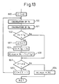
- the flowchart shown in Fig. 13 has an additional function, which is able to avoid a frequent brightness change derived from a temporarily frequency changes of an input signal, in addition to the function of the process shown in Fig. 11 , which overcomes the extraordinary display problem by reducing the number of scan lines.
- This function is based on the same necessity as that of the first embodiment, and therefore, the explanation thereof will not be repeated here.
- new steps 600, 601, 602, 603 and 604 are added to the flowchart of the process shown in Fig. 11 , wherein step 600 is to reset counter CT to 0, step 601 to set counter CT to be a predetermined value F, step 602 to judge whether counter CT is 0 or not, step 603 to decrement counter CT by one, and step 604 to reset the corrected number of scan lines NLmax, obtained by conducting steps 100 to 103 and 400, to the original number of scan lines NL.
- the first and second embodiments mentioned above are also effective as a supplemental technique for the existing countermeasures against a multi-scanning mode.
- a PDP having a multi-Vsync function which is to reduce the number of subframes in synchronizing with the period of a vertical synchronizing signal (Vsync).
- This function can, however, adjust the length of a driving period using only the minimum subframe, for example, SF1, as one unit, thus resulting in a rough adjustment.
- SF1 vertical synchronizing signal
- a fine adjustment is possible by applying the present invention.
- This provides a PDP having a high applicability to a wide range of frequency, in addition to the effect of reducing the number of the subframes.
- the display brightness of a PDP changes according to the frequency change of an input signal from an external device, to which the PDP is connected.
- an event occurs in which one image is displayed with a different brightness when a PDP is connected to a different external device, although the image essentially has the same brightness.
- the flowchart shown in Fig. 14a shows a process designed to cope with such an event.
- one frame length Tv is first calculated from one period of an input synchronizing signal at step 100. Thereafter, at step 700, the maximum number of sustaining pulses Nsus(Tv), which can be applied during the one frame length Tv without causing an extraordinary display, is calculated based on the frame length Tv obtained in step 100. By multiplying Ysus, which is of a brightness of one sustaining pulse, by Nsus(Tv), the maximum brightness Ymax which can be displayed without causing any extraordinary display is obtained.
- a brightness to be a reference value predetermined brightness Yc
- predetermined brightness Yc has been set in advance in order to fix the display brightness constant without depending on the frequencies of input signals.
- step 701 the obtained maximum brightness Ymax and the predetermined brightness Yc are compared.
- the process moves to step 702 in which correction of the present number of sustaining pulses is conducted to make it agree with the predetermined brightness Yc.
- the predetermined brightness Yc is subtracted from the maximum brightness Ymax and the difference is divided by brightness Ysus for one sustaining pulse, thus obtaining a correction value of the total number of sustaining pulses.
- this correction value is subtracted from Nsus, which is the number of sustaining pulses capable of being displayed, and as a result, the number of sustaining pulses corresponding to the predetermined brightness Yc is obtained.
- Fig. 14b shows the structure of the common driver control part 29 shown in Fig. 5a , which structure is designed especially to realize the fifth process.
- common driver control part 29 includes the frame length calculating circuit 10 for conducting the step 100, a maximum number of sustaining pulse and maximum brightness calculating circuit 291 for conducting the step 700, an agreement detecting circuit 292 for conducting the step 701, and a maximum number of sustaining pulse setting circuit 293 for conducting the step 702 shown in Fig. 14a .
- These circuits 10, 291, 292, 293 and 294 are, of cause, structured with the MPU 29a and the memory 29c shown in Fig. 6 .
- the present invention is capable of improving the display quality of a PDP by so adjusting the total number of sustaining pulses that an image is displayed with the same brightness regardless that what kind of external device is connected to the PDP.
- a plasma display device embodying the present invention is capable of conducting an ordinary display even if it is connected to an external device driven by a different frequency. This is because the plasma display device can adjust the total number of sustaining pulses or the number of scanning lines so that the relationship between the frame length and the driving period length becomes proper. Thus, it becomes possible to provide a plasma display device having a high applicability to a variety of external devices.
Claims (10)
- Dispositif d'affichage à plasma comprenant :un panneau d'affichage à plasma (2) ;une partie d'entraînement (21-25) servant à entraîner le panneau d'affichage à plasma (2) en un mode sous-trames dans lequel une trame d'affichage est divisée en une pluralité de sous-trames et un nombre prédéterminé d'impulsions de soutien sont appliquées au panneau d'affichage à plasma (20) pendant chacune des sous-trames de manière à provoquer une décharge de soutien ; etun moyen de commande d'entraînement (29) servant à commander ladite partie d'entraînement, incluant :caractérisé en ce que :un moyen de détection de nombre d'impulsions de soutien (11) servant à obtenir, à partir d'informations de luminosité de trame contenues dans un signal d'image, un nombre total d'impulsions de soutien à appliquer dans une trame ;un moyen de calcul de longueur de trame (10) servant à calculer une longueur d'une trame d'affichage selon une période d'un signal de synchronisation verticale qui est entré depuis un dispositif externe avec ledit signal d'image,un moyen de calcul de longueur de période d'entraînement (12) servant à calculer une longueur d'une période d'entraînement du panneau d'affichage à plasma (20) nécessaire pour afficher une trame sur la base du nombre total d'impulsions de soutien obtenu par ledit moyen de détection de nombre d'impulsions de soutien (11),un moyen de comparaison (14) servant à comparer les résultats respectifs provenant dudit moyen de calcul de longueur de trame (10) et dudit moyen de calcul de longueur de période d'entraînement (12), etun moyen de changement (16) servant à changer un nombre total d'impulsions de soutien dans une trame selon un résultat comparé dans ledit moyen de comparaison (14);ledit moyen de commande d'entraînement (29) comprend en outre un moyen de détection d'intervalle de temps (18) servant à détecter un intervalle d'une période prédéterminée dans lequel aucun changement n'est détecté une fois que ledit moyen de comparaison (14) a détecté un changement dans le résultat comparé, et dans lequel ledit moyen de changement (16) est agencé pour changer le nombre total d'impulsions de soutien après que ledit moyen de détection d'intervalle de temps (18) a détecté l'intervalle de la période prédéterminée.
- Dispositif d'affichage à plasma selon la revendication 1, dans lequel ledit moyen de changement (16) est agencé pour changer le nombre total d'impulsions de soutien de manière à réduire celui-ci lorsque ledit moyen de comparaison (14) trouve que la longueur d'une trame obtenue par le moyen de calcul de longueur de trame (10) est plus courte que la longueur d'une période d'entraînement obtenue par le moyen de calcul de longueur de période d'entraînement (12).
- Dispositif d'affichage à plasma selon la revendication 1, dans lequel ledit moyen de changement (16) est agencé pour changer le nombre total d'impulsions de soutien de manière à augmenter celui-ci lorsque ledit moyen de comparaison (14) trouve que la longueur d'une trame obtenue par le moyen de calcul de longueur de trame (10) est plus longue que la longueur d'une période d'entraînement obtenue par le moyen de calcul de longueur de période d'entraînement (12).
- Dispositif d'affichage à plasma selon la revendication 1, dans lequel ledit moyen de calcul de longueur de trame (10), ledit moyen de calcul de longueur de période d'entraînement (12), ledit moyen de comparaison (14), et ledit moyen de détection d'intervalle de temps (18) sont fournis par une unité microprocesseur (29a) et un support d'enregistrement (29c) dans lequel est stocké un programme servant à amener ladite unité microprocesseur (29a) à fonctionner en tant que lesdits moyens (10, 12, 14, 18).
- Dispositif d'affichage à plasma selon l'une quelconque des revendications précédentes,
dans lequel ledit moyen de commande d'entraînement (29) comprend en outre une table ROM (29d) comportant une pluralité d'adresses dans laquelle est stockée une combinaison de nombres d'impulsions de soutien pour les sous-trames respectives,
ledit moyen de détection de nombre d'impulsions de soutien (11) est agencé pour détecter ledit nombre total d'impulsions de soutien contenues dans une trame sur la base d'une adresse de ladite table ROM (29d), ladite adresse correspondant auxdites informations de luminosité contenues dans ledit signal d'image. - Dispositif d'affichage à plasma selon la revendication 5, dans lequel ledit moyen de changement (16) est agencé pour changer le nombre total d'impulsions de soutien dans une trame en changeant une adresse de la table ROM (29d).
- Dispositif d'affichage à plasma comprenant :un panneau d'affichage à plasma (20) comportant une pluralité de cellules électroluminescentes agencées sous la forme d'une matrice ;une partie d'entraînement (21-25) servant à entraîner le panneau d'affichage à plasma (20) en un mode sous-trames dans lequel une trame d'affichage est divisée en une pluralité de sous-trames et un nombre prédéterminé d'impulsions de soutien sont appliquées à ladite pluralité de cellules électroluminescentes dans chaque sous-trame tout en balayant la pluralité de cellules électroluminescentes de manière séquentiellement linéaire ; etun moyen de commande d'entraînement (29) servant à commander ladite partie d'entraînement, incluant :un moyen de détection de nombre d'impulsions de soutien (11) servant à obtenir, à partir d'informations de luminosité contenues dans un signal d'image, un nombre total d'impulsions de soutien à appliquer dans une trame ;un moyen de calcul de longueur de trame (10) servant à calculer une longueur d'une trame d'affichage selon une période d'un signal de synchronisation verticale qui est introduit depuis un dispositif externe avec ledit signal d'image ;un moyen de calcul de longueur de période d'entraînement (12) servant à calculer une longueur d'une période d'entraînement du panneau d'affichage à plasma (20) nécessaire pour afficher une trame sur la base du nombre total d'impulsions de soutien détecté par ledit moyen de détection de nombre d'impulsions de soutien (11), etun moyen de comparaison (14) servant à comparer les résultats provenant dudit moyen de calcul de longueur de trame (10) et dudit moyen de calcul de longueur de période d'entraînement (12) ; caractérisé en ce que ledit moyen de commande d'entraînement (29) comprend en outre :un moyen de changement (16) servant à changer un nombre total de lignes de balayage, qui sont balayées de manière séquentiellement linéaire, selon un résultat comparé provenant dudit moyen de comparaison (14) ; etun moyen de détection d'intervalle de temps (18) servant à détecter un intervalle d'une période prédéterminée pendant lequel aucun changement n'est détecté une fois que ledit moyen de comparaison (14) a détecté un changement dans le résultat comparé, et dans lequel ledit moyen de changement (16) est agencé pour changer le nombre total de lignes de balayage après que ledit moyen de détection d'intervalle de temps (18) a détecté l'intervalle de la période prédéterminée.
- Dispositif d'affichage à plasma selon la revendication 7, dans lequel ledit moyen de changement (16) est agencé pour changer le nombre total de lignes de balayage de manière à réduire celui-ci lorsque ledit moyen de comparaison (14) trouve que la longueur d'une trame obtenue par le moyen de calcul de longueur de trame (10) est plus courte que la longueur d'une période d'entraînement obtenue par le moyen de calcul de longueur de période d'entraînement (12).
- Dispositif d'affichage à plasma selon la revendication 7, dans lequel ledit moyen de changement (16) est agencé pour changer le nombre total de lignes de balayage de manière à augmenter celui-ci lorsque ledit moyen de comparaison (14) trouve que la longueur d'une trame obtenue par le moyen de calcul de longueur de trame (10) est plus longue que la longueur d'une période d'entraînement obtenue par le moyen de calcul de longueur de période d'entraînement (12).
- Dispositif d'affichage à plasma selon la revendication 7, dans lequel ledit moyen de calcul de longueur de trame (10), ledit moyen de calcul de longueur de période d'entraînement (12), ledit moyen de comparaison (14), et ledit moyen de détection d'intervalle de temps (18) sont fournis par une unité microprocesseur (29a) et un support d'enregistrement (29c) dans lequel est stocké un programme servant à amener ladite unité microprocesseur (29a) à fonctionner en tant que lesdits moyens (10, 12, 14, 18).
Applications Claiming Priority (4)
| Application Number | Priority Date | Filing Date | Title |
|---|---|---|---|
| JP31572196 | 1996-11-27 | ||
| JP315721/96 | 1996-11-27 | ||
| JP21231697A JP3672697B2 (ja) | 1996-11-27 | 1997-08-06 | プラズマディスプレイ装置 |
| JP212316/97 | 1997-08-06 |
Publications (2)
| Publication Number | Publication Date |
|---|---|
| EP0845769A1 EP0845769A1 (fr) | 1998-06-03 |
| EP0845769B1 true EP0845769B1 (fr) | 2008-02-13 |
Family
ID=26519146
Family Applications (1)
| Application Number | Title | Priority Date | Filing Date |
|---|---|---|---|
| EP97307874A Expired - Lifetime EP0845769B1 (fr) | 1996-11-27 | 1997-10-06 | Dispositif d'affichage à plasma contrôlé en mode sous trames |
Country Status (6)
| Country | Link |
|---|---|
| US (1) | US6072448A (fr) |
| EP (1) | EP0845769B1 (fr) |
| JP (1) | JP3672697B2 (fr) |
| KR (1) | KR100260590B1 (fr) |
| DE (1) | DE69738510T2 (fr) |
| TW (1) | TW346615B (fr) |
Cited By (1)
| Publication number | Priority date | Publication date | Assignee | Title |
|---|---|---|---|---|
| CN107978274A (zh) * | 2016-10-25 | 2018-05-01 | 乐金显示有限公司 | 显示装置及其驱动方法 |
Families Citing this family (39)
| Publication number | Priority date | Publication date | Assignee | Title |
|---|---|---|---|---|
| TW371386B (en) * | 1996-12-06 | 1999-10-01 | Matsushita Electric Ind Co Ltd | Video display monitor using subfield method |
| US6133689A (en) * | 1997-12-31 | 2000-10-17 | Micron Technology, Inc. | Method and apparatus for spacing apart panels in flat panel displays |
| EP0983584A2 (fr) * | 1998-03-23 | 2000-03-08 | Koninklijke Philips Electronics N.V. | Commande d'affichage |
| JP3421578B2 (ja) * | 1998-06-11 | 2003-06-30 | 富士通株式会社 | Pdpの駆動方法 |
| JP3424587B2 (ja) | 1998-06-18 | 2003-07-07 | 富士通株式会社 | プラズマディスプレイパネルの駆動方法 |
| EP1012817B1 (fr) * | 1998-07-10 | 2006-06-07 | Orion Electric Co., Ltd. | Procede de commande d'un panneau d'affichage a plasma a courant alternatif permettant la creation de gradations de niveau de gris |
| US6359604B1 (en) | 1998-08-20 | 2002-03-19 | Micron Technology, Inc. | Matrix addressable display having pulse number modulation |
| JP3556103B2 (ja) * | 1998-09-18 | 2004-08-18 | 富士通株式会社 | Pdpの駆動方法 |
| US6597331B1 (en) * | 1998-11-30 | 2003-07-22 | Orion Electric Co. Ltd. | Method of driving a plasma display panel |
| KR100284340B1 (ko) * | 1999-02-27 | 2001-03-02 | 김순택 | 플라즈마 표시 패널의 구동방법 |
| JP2000259116A (ja) * | 1999-03-09 | 2000-09-22 | Nec Corp | 多階調表示プラズマディスプレイの駆動方法および装置 |
| TW480727B (en) * | 2000-01-11 | 2002-03-21 | Semiconductor Energy Laboratro | Semiconductor display device |
| US20010030511A1 (en) * | 2000-04-18 | 2001-10-18 | Shunpei Yamazaki | Display device |
| JP2001352460A (ja) * | 2000-06-09 | 2001-12-21 | Pioneer Electronic Corp | プラズマディスプレイ装置用の赤外線リモートコントロール装置 |
| TW512304B (en) * | 2000-06-13 | 2002-12-01 | Semiconductor Energy Lab | Display device |
| JP3556163B2 (ja) | 2000-09-25 | 2004-08-18 | 富士通日立プラズマディスプレイ株式会社 | 表示装置 |
| JP4707887B2 (ja) * | 2001-07-11 | 2011-06-22 | パナソニック株式会社 | 表示制御装置及び表示装置 |
| JP4851663B2 (ja) * | 2001-07-19 | 2012-01-11 | パナソニック株式会社 | 表示パネルの輝度制御方法 |
| JP2003043991A (ja) * | 2001-08-02 | 2003-02-14 | Fujitsu Hitachi Plasma Display Ltd | プラズマディスプレイ装置 |
| KR100441523B1 (ko) * | 2001-09-28 | 2004-07-23 | 삼성에스디아이 주식회사 | 플라즈마 표시 패널의 소비 전력을 제어하는 방법 및 장치 |
| KR100472359B1 (ko) * | 2001-11-28 | 2005-02-21 | 엘지전자 주식회사 | 평균 휘도 레벨 설정방법 |
| EP1329869A1 (fr) * | 2002-01-16 | 2003-07-23 | Deutsche Thomson-Brandt Gmbh | Procédé et dispositif de traitement d'images vidéo, |
| JP4308488B2 (ja) * | 2002-03-12 | 2009-08-05 | 日立プラズマディスプレイ株式会社 | プラズマディスプレイ装置 |
| TWI250492B (en) * | 2002-10-24 | 2006-03-01 | Pioneer Corp | Driving apparatus of display panel |
| US6784898B2 (en) * | 2002-11-07 | 2004-08-31 | Duke University | Mixed mode grayscale method for display system |
| JP4636857B2 (ja) * | 2004-05-06 | 2011-02-23 | パナソニック株式会社 | プラズマディスプレイ装置 |
| EP1751734A4 (fr) | 2004-05-21 | 2007-10-17 | Semiconductor Energy Lab | Dispositif d'affichage et instrument électronique |
| JP4351591B2 (ja) * | 2004-07-07 | 2009-10-28 | 富士通株式会社 | サーバシステムおよびサーバ |
| US7936364B2 (en) * | 2004-08-17 | 2011-05-03 | Intel Corporation | Maintaining balance in a display |
| US8194006B2 (en) | 2004-08-23 | 2012-06-05 | Semiconductor Energy Laboratory Co., Ltd. | Display device, driving method of the same, and electronic device comprising monitoring elements |
| US20070035488A1 (en) * | 2004-12-03 | 2007-02-15 | Semiconductor Energy Laboratory Co., Ltd. | Driving method of display device |
| US20060139265A1 (en) * | 2004-12-28 | 2006-06-29 | Semiconductor Energy Laboratory Co., Ltd. | Driving method of display device |
| JPWO2007015308A1 (ja) * | 2005-08-04 | 2009-02-19 | 日立プラズマディスプレイ株式会社 | プラズマディスプレイ装置 |
| EP1785973A1 (fr) * | 2005-11-10 | 2007-05-16 | Deutsche Thomson-Brandt Gmbh | Procédé et appareil pour le contrôle du niveau de puissance dans un dispositif d'affichage |
| KR100761120B1 (ko) * | 2005-11-23 | 2007-09-21 | 엘지전자 주식회사 | 플라즈마 디스플레이 장치 |
| CN103794173A (zh) * | 2011-12-31 | 2014-05-14 | 四川虹欧显示器件有限公司 | 等离子显示设备的显示方法及装置 |
| CN102956188A (zh) * | 2012-12-11 | 2013-03-06 | 四川虹欧显示器件有限公司 | 一种驱动等离子显示设备的方法和装置 |
| CN102956189A (zh) * | 2012-12-11 | 2013-03-06 | 四川虹欧显示器件有限公司 | 一种驱动等离子显示设备的方法和装置 |
| JP6705208B2 (ja) * | 2016-02-26 | 2020-06-03 | 日亜化学工業株式会社 | 表示方法 |
Citations (1)
| Publication number | Priority date | Publication date | Assignee | Title |
|---|---|---|---|---|
| US5724053A (en) * | 1994-09-07 | 1998-03-03 | Pioneer Electronic Corporation | Plasma display apparatus adapted to multiple frequencies |
Family Cites Families (8)
| Publication number | Priority date | Publication date | Assignee | Title |
|---|---|---|---|---|
| JP2892009B2 (ja) * | 1988-05-28 | 1999-05-17 | 株式会社東芝 | 表示制御方式 |
| JP2932686B2 (ja) * | 1990-11-28 | 1999-08-09 | 日本電気株式会社 | プラズマディスプレイパネルの駆動方法 |
| JPH0535205A (ja) * | 1991-07-29 | 1993-02-12 | Nec Corp | プラズマデイスプレイの駆動方式 |
| US5943032A (en) * | 1993-11-17 | 1999-08-24 | Fujitsu Limited | Method and apparatus for controlling the gray scale of plasma display device |
| JP2856241B2 (ja) * | 1993-11-17 | 1999-02-10 | 富士通株式会社 | プラズマディスプレイ装置の階調制御方法 |
| JP2853537B2 (ja) * | 1993-11-26 | 1999-02-03 | 富士通株式会社 | 平面表示装置 |
| JP3555995B2 (ja) * | 1994-10-31 | 2004-08-18 | 富士通株式会社 | プラズマディスプレイ装置 |
| KR100362432B1 (ko) * | 1995-09-12 | 2003-01-29 | 삼성에스디아이 주식회사 | 플라즈마표시소자의구동방법 |
-
1997
- 1997-08-06 JP JP21231697A patent/JP3672697B2/ja not_active Expired - Fee Related
- 1997-09-30 US US08/941,107 patent/US6072448A/en not_active Expired - Lifetime
- 1997-10-04 TW TW086114526A patent/TW346615B/zh not_active IP Right Cessation
- 1997-10-06 DE DE69738510T patent/DE69738510T2/de not_active Expired - Lifetime
- 1997-10-06 EP EP97307874A patent/EP0845769B1/fr not_active Expired - Lifetime
- 1997-10-28 KR KR1019970055483A patent/KR100260590B1/ko not_active IP Right Cessation
Patent Citations (1)
| Publication number | Priority date | Publication date | Assignee | Title |
|---|---|---|---|---|
| US5724053A (en) * | 1994-09-07 | 1998-03-03 | Pioneer Electronic Corporation | Plasma display apparatus adapted to multiple frequencies |
Cited By (1)
| Publication number | Priority date | Publication date | Assignee | Title |
|---|---|---|---|---|
| CN107978274A (zh) * | 2016-10-25 | 2018-05-01 | 乐金显示有限公司 | 显示装置及其驱动方法 |
Also Published As
| Publication number | Publication date |
|---|---|
| JP3672697B2 (ja) | 2005-07-20 |
| KR19980041967A (ko) | 1998-08-17 |
| DE69738510D1 (de) | 2008-03-27 |
| US6072448A (en) | 2000-06-06 |
| KR100260590B1 (ko) | 2000-07-01 |
| DE69738510T2 (de) | 2009-02-05 |
| EP0845769A1 (fr) | 1998-06-03 |
| TW346615B (en) | 1998-12-01 |
| JPH10214059A (ja) | 1998-08-11 |
Similar Documents
| Publication | Publication Date | Title |
|---|---|---|
| EP0845769B1 (fr) | Dispositif d'affichage à plasma contrôlé en mode sous trames | |
| US6483251B2 (en) | Method of driving plasma display | |
| US6630796B2 (en) | Method and apparatus for driving a plasma display panel | |
| JP3993216B2 (ja) | 高コントラストプラズマディスプレイ | |
| KR100436452B1 (ko) | 표시데이터량에 따라 유지방전펄스 수를 조정하는 패널표시장치 및 그 구동방법 | |
| US6720940B2 (en) | Method and device for driving plasma display panel | |
| KR100780065B1 (ko) | Ac형 pdp의 구동 장치 및 표시 장치 | |
| US7535438B2 (en) | Plasma display apparatus with increased peak luminance | |
| US20090167642A1 (en) | Method and apparatus for driving plasma display panel | |
| JPH07140928A (ja) | プラズマディスプレイ装置の階調制御方法 | |
| US5724053A (en) | Plasma display apparatus adapted to multiple frequencies | |
| US6756977B2 (en) | Display device and method of driving a display panel | |
| EP1150272A2 (fr) | Méthode de commande d'un panneau d'affichage à plasma à courant alternatif | |
| US20070001932A1 (en) | Plasma display device and method of treating the same | |
| KR20000001748A (ko) | 플라즈마 디스플레이 패널의 구동장치 및 방법 | |
| KR20000003328A (ko) | Pdp의 유지방전펄스수 증가에 따른 밝기 보상방법 | |
| JP2010049108A (ja) | プラズマディスプレイパネルの駆動方法 |
Legal Events
| Date | Code | Title | Description |
|---|---|---|---|
| PUAI | Public reference made under article 153(3) epc to a published international application that has entered the european phase |
Free format text: ORIGINAL CODE: 0009012 |
|
| AK | Designated contracting states |
Kind code of ref document: A1 Designated state(s): DE FR GB NL |
|
| AX | Request for extension of the european patent |
Free format text: AL;LT;LV;RO;SI |
|
| 17P | Request for examination filed |
Effective date: 19981009 |
|
| AKX | Designation fees paid |
Free format text: DE FR GB NL |
|
| RBV | Designated contracting states (corrected) |
Designated state(s): DE FR GB NL |
|
| 17Q | First examination report despatched |
Effective date: 20050415 |
|
| RAP1 | Party data changed (applicant data changed or rights of an application transferred) |
Owner name: HITACHI, LTD. |
|
| RAP1 | Party data changed (applicant data changed or rights of an application transferred) |
Owner name: HITACHI PLASMA PATENT LICENSING CO., LTD. |
|
| GRAP | Despatch of communication of intention to grant a patent |
Free format text: ORIGINAL CODE: EPIDOSNIGR1 |
|
| GRAS | Grant fee paid |
Free format text: ORIGINAL CODE: EPIDOSNIGR3 |
|
| GRAA | (expected) grant |
Free format text: ORIGINAL CODE: 0009210 |
|
| AK | Designated contracting states |
Kind code of ref document: B1 Designated state(s): DE FR GB NL |
|
| REG | Reference to a national code |
Ref country code: GB Ref legal event code: FG4D |
|
| REF | Corresponds to: |
Ref document number: 69738510 Country of ref document: DE Date of ref document: 20080327 Kind code of ref document: P |
|
| ET | Fr: translation filed | ||
| PLBE | No opposition filed within time limit |
Free format text: ORIGINAL CODE: 0009261 |
|
| STAA | Information on the status of an ep patent application or granted ep patent |
Free format text: STATUS: NO OPPOSITION FILED WITHIN TIME LIMIT |
|
| 26N | No opposition filed |
Effective date: 20081114 |
|
| PGFP | Annual fee paid to national office [announced via postgrant information from national office to epo] |
Ref country code: NL Payment date: 20101016 Year of fee payment: 14 Ref country code: FR Payment date: 20101020 Year of fee payment: 14 |
|
| PGFP | Annual fee paid to national office [announced via postgrant information from national office to epo] |
Ref country code: DE Payment date: 20100929 Year of fee payment: 14 |
|
| PGFP | Annual fee paid to national office [announced via postgrant information from national office to epo] |
Ref country code: GB Payment date: 20101006 Year of fee payment: 14 |
|
| REG | Reference to a national code |
Ref country code: NL Ref legal event code: V1 Effective date: 20120501 |
|
| GBPC | Gb: european patent ceased through non-payment of renewal fee |
Effective date: 20111006 |
|
| REG | Reference to a national code |
Ref country code: FR Ref legal event code: ST Effective date: 20120629 |
|
| PG25 | Lapsed in a contracting state [announced via postgrant information from national office to epo] |
Ref country code: NL Free format text: LAPSE BECAUSE OF NON-PAYMENT OF DUE FEES Effective date: 20120501 Ref country code: DE Free format text: LAPSE BECAUSE OF NON-PAYMENT OF DUE FEES Effective date: 20120501 |
|
| REG | Reference to a national code |
Ref country code: DE Ref legal event code: R119 Ref document number: 69738510 Country of ref document: DE Effective date: 20120501 |
|
| PG25 | Lapsed in a contracting state [announced via postgrant information from national office to epo] |
Ref country code: FR Free format text: LAPSE BECAUSE OF NON-PAYMENT OF DUE FEES Effective date: 20111102 Ref country code: GB Free format text: LAPSE BECAUSE OF NON-PAYMENT OF DUE FEES Effective date: 20111006 |