EP0844754B1 - Vorrichtung zur Multiplexierung und Demultiplexierung von Daten - Google Patents
Vorrichtung zur Multiplexierung und Demultiplexierung von Daten Download PDFInfo
- Publication number
- EP0844754B1 EP0844754B1 EP97120466A EP97120466A EP0844754B1 EP 0844754 B1 EP0844754 B1 EP 0844754B1 EP 97120466 A EP97120466 A EP 97120466A EP 97120466 A EP97120466 A EP 97120466A EP 0844754 B1 EP0844754 B1 EP 0844754B1
- Authority
- EP
- European Patent Office
- Prior art keywords
- data
- microprocessor
- shift
- register
- accordance
- Prior art date
- Legal status (The legal status is an assumption and is not a legal conclusion. Google has not performed a legal analysis and makes no representation as to the accuracy of the status listed.)
- Expired - Lifetime
Links
Images


Classifications
-
- H—ELECTRICITY
- H04—ELECTRIC COMMUNICATION TECHNIQUE
- H04J—MULTIPLEX COMMUNICATION
- H04J3/00—Time-division multiplex systems
- H04J3/02—Details
- H04J3/06—Synchronising arrangements
- H04J3/0602—Systems characterised by the synchronising information used
- H04J3/0605—Special codes used as synchronising signal
-
- H—ELECTRICITY
- H04—ELECTRIC COMMUNICATION TECHNIQUE
- H04J—MULTIPLEX COMMUNICATION
- H04J3/00—Time-division multiplex systems
- H04J3/02—Details
- H04J3/04—Distributors combined with modulators or demodulators
- H04J3/047—Distributors with transistors or integrated circuits
Definitions
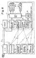
- the protocol analyzing/data separating section 1032 is formed by bit synchronism detectors 1031-1, 1031-2, ⁇ , 1031-k, and a protocol processing section 1032.
- the protocol processing section 1032 is hierarchically configured to detect a bit string to a synchronization pattern at high speed.
- the protocol processing section 1032 is constructed by protocol processing units 1032-1, 1032-2, ..., 1032-m, 1032-1-1, 1032-1-2, ..., 1032-1-n, 1032-2-1, ⁇ , 1032-2-n, and so on.
- Figs. 7A and 7B show typical bit arrangements using 2B channels of an ISDN, where audio data is framed in accordance with the H.221 Standard where low speed data (LSD) is 1,200 bps (G.722) and multilayered protocol (MLP) is 4 kbps (G.722).
- Figs. 8A and 8B show typical bit arrangements using 2B channels of an ISDN by switching G.722 of Figs. 7A and 7B to G.728 (ITU Standard).
- the bits on the 2B channels can be classified into 12 pattern types A, B, ⁇ , H of these pattern types, the combinations that are not allowed to appear by the H.221 standards can be deleted to finally obtain the following ten combinations of pattern types: A + G, A + H, B + H, C + G, C + H, D + H, E + G, E + H, F + G and F + N.
- the bit separation auxiliary circuit 4 of Fig. 6 is constructed more concretely as illustrated in Fig. 12. That is, the data shift register 41 of Fig. 6 is constructed by a 16-bit shift register 411, a 7-bit shift register 412 and a selector 413.
- the correction register 42 of Fig. 6 is constructed by a shift position register 421 and a shift control circuit 422. Also, the group of the shift registers 47-1, 47-2, ⁇ , 47-X of Fig. 6 are a group of a 24-bit shift register 47-1, an 8-bit shift register 47-2, an 8-bit shift register 47-3, an 8-bit shift register 47-4 and an 8-bit shift register 47-5. Further, a 3-bit counter 48 is added to generates a carry signal as an acknowledgement signal ACK.
- the 8-bit shift registers 47-2, 47-3, 47-4 and 47-5 are provided for the data S1, S2, S3 and S4, whereas the 24-bit shift register 47-1 is provided for the remaining data, i.e., video data and audio data.
- the procedure for separating data is divided into a synchronism phase and a separation phase in the same way as in the second prior art data demultiplexing apparatus.
- the microprocessor 2' detects synchronous patterns from the input data. To begin with, the bit separated pattern of the initial channel is processed as the pattern type C or E. In this case, the microprocessor 2' slices the data input to the data demultiplexing apparatus into data of 1 bit ⁇ 8 for the subchannel and outputs it. Also, the microprocessor 2' checks the content of the shift registers 47-1, 47-2, ⁇ , 47-5 each time it transmits data to the data demultiplexing apparatus, in order to check if a synchronous pattern is appearing there.
- the data can be checked for all the subchannels, or subchannesl 1 through 8, by repeating the above operation four times to obtained the overall shift amount.
- the obtained shift amount is then set in shift position register 421 for controlling the overall shift amount.
- one of the ten separated patterns is selected as information obtained by the protocol and the data demultiplexing apparatus is notified of it. Thereafter, predetermined data are sent to the data demultiplexing apparatus to produce separated data.
- the microprocessor 9 specifies a pattern for data to be multiplexed to a pointer specifying register 111 of a LUT ROM 113.
- the pattern is obtained by combining types A through F and types G and H of Figs. 10 and 11.
- the data to be multiplexed will be written into a 24-bit shift register 115-1 and 8-bit shift registers 115-2, 115-3, 115-4 and 115-5 by the microprocessor 9.
- the data stored in the LUT ROM 118 as shift amounts representing bit patterns are sequentially read by a counter 112 at the address specified by the pointer specifying register 111.
- the data read from the LUT ROM 113 are then entered into a decoder 114 for selecting and controlling one of the shift registers 115-1, 115-2, ⁇ , 115-5 to be operated, so that the selected register is driven to operate. Additionally, a data selector 116 selects the output data of the selected shift register to be multiplexed and transmits the data to a 16-bit shift register 118.
- the number of data sent out from the 24-bit shift register 115-1 is counted by a 3-bit counter 117, which notifies the microprocessor 9 of each 8-bit shift and requests a new 8-bit data.
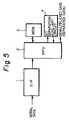
- a serial-to-parallel converter 1(8) is duplex, and a bit multiplexing/separation anxiliary circuit 4(11) serves as the separation auxiliary circuit 4 of Fig. 5 as well as the multiplexing auxiliary circuit 11 of Fig. 11.
- the bit multiplexing/Separation auxiliary circuit 4(11) is illustrated in Fig. 16.
- the shift registers 47-1(115-1), 47-2(115-2), 47-3(115-3), 47-4(115-4) and 47-5(115-5) are duplex, and the 16-bit shift register 411(118) is also duplex.
- shift registers optimized for a protocol
- an LUT ROM for storing the data framing rule drawn out of the pattern of the protocol
- selectors-to be switched by the data output from the LUT ROM and a microprocessor the load of the software can be relieved without damaging the flexibility of the software system.
Landscapes
- Engineering & Computer Science (AREA)
- Computer Networks & Wireless Communication (AREA)
- Signal Processing (AREA)
- Microelectronics & Electronic Packaging (AREA)
- Time-Division Multiplex Systems (AREA)
- Synchronisation In Digital Transmission Systems (AREA)
Claims (4)
- Datenmultiplex/-demultiplexvorrichtung, welche folgendes aufweist:wobei der Mikroprozessor folgendes aufweist:einen Serien-Parallel-Umsetzer (1) sowie einen Parallel-Serien-Umsetzer (8) für das Umsetzen von seriellen Daten in parallele Daten;einen Mikroprozessor (2');einen Speicher (3) für das temporäre Speichern der parallelen Daten mit Hilfe des Mikroprozessors;ein an den Mikroprozessor angeschlossenes Daten-Schieberegister (41) für die Eingabe von Daten aus dem Speicher mit Hilfe des Mikroprozessors;ein an das Daten-Schieberegister und den Mikroprozessor angeschlossenes Korrekturregister (42) für die Speicherung einer Schiebekorrekturmenge auf einem Übertragungsweg des Daten-Schieberegisters, wobei die Schiebekorrekturmenge durch den Mikroprozessor bestimmt wird;ein an dem Mikroprozessor angeschlossenes Rahmenvorschriften-Register (43) für die Speicherung einer vom Mikroprozessor festgelegten Rahmenvorschrift;ein an das Rahmenvorschriften-Register angeschlossener Zähler (44) für die Ausführung einer Zähloperation entsprechend der Rahmenvorschrift und für die Ausgabe eines Adressinformationssignals;eine an den Zähler angeschlossene Nachschlagetabelle (45) für die Ausgabe eines Selektor-Wahlsignals entsprechend dem Adressinformationssignal;eine Vielzahl von Schieberegistern (47-1, 47-2, ..., 47-X); undeinen zwischen dem Daten-Schieberegister und der Vielzahl von Schieberegistern sowie an die Nachschlagetabelle ROM angeschlossenen Datenselektor (46) für die Verteilung der Ausgabedaten des Daten-Schieberegisters unter der Vielzahl von Schieberegistern entsprechend dem Selektor-Wahlsignal,eine Vorrichtung für die Analyse der Daten, die von der Vielzahl von Schieberegistern getrennt werden, und für die Ausführung einer Synchronisierungs-Erfassungsoperation und einer Protokollbestimmungsoperation; undeine Vorrichtung für die Bestimmung der Rahmenvorschrift des Rahmenvorschriften-Registers entsprechend einem Ergebnis der Protokollbestimmungsoperation.
- Vorrichtung nach Anspruch 1, dadurch gekennzeichnet, dass der Serien-Parallel-Umsetzer, das Daten-Schieberegister und die Vielzahl von Schieberegistern doppelt ausgebildet sind, wobei die Vorrichtung ferner folgendes aufweist:wobei die Vorrichtung so angepasst ist, dass sie Daten entsprechend der Rahmenvorschrift zur Erzeugung von Multiplexdaten synthesiert.einen zwischen der Nachschlagetabelle ROM und der Vielzahl von Schieberegistern angeschlossener Decoder (114) für die Selektion und Steuerung eines aus der Vielzahl von Schieberegistern entsprechend dem Selektor-Wahlsignal; undeinen zusätzlichen Datenselektor (112), der zwischen der Vielzahl von Schieberegistern und dem Daten-Schieberegister angeschlossen ist;
- Datendemultiplex-Vorrichtung, welche folgendes aufweist:wobei der Prozessor mit Hilfe von Programmen zur Erfassung einer Synchronisierung, zur Analyse eines Protokolls und zur Trennung von Daten entsprechend einer Rahmenvorschrift gesteuert wird.einen Serien-Parallel-Umsetzer (1) für die Umsetzung von seriellen Daten in parallele Daten;einen Prozessor (2') für den Empfang der parallelen Daten;einen Speicher (3) für die temporäre Speicherung der parallelen Daten mit Hilfe des Prozessors;einen an den Prozessor angeschlossenen Bittrennungs-Hilfsschaltkreis (4), welcher ein Daten-Schieberegister (41) für den Empfang von parallen Daten, eine Nachschlagetabelle (45) für die Speicherung einer Rahmenvorschrift in Form eines Selektionssignals, sowie einen Selektor (46) umfasst, der mit dem Daten-Schieberegister und der Vielzahl von Schieberegistern (47-1, 47-2, ...) für die Zuteilung der Ausgabedaten des Daten-Schieberegisters unter der Vielzahl von Schieberegistern verbunden ist,
- Datenmultiplexvorrichtung, welche folgendes aufweist:wobei die Vorrichtung so angepasst ist, dass ein Multiplexen der Daten entsprechend der Rahmenvorschrift erfolgt und Multiplexdaten erzeugt werden.einen Parallel-Serien-Umsetzer (8),einen an den Parallel-Serien-Umsetzer angeschlossenen Mikroprozessor (9),ein an den Mikroprozessor angeschlossenes Zeiger-Spezifizierregister für die Speicherung einer von dem Mikroprozessor bestimmten Rahmenvorschrift;ein an das Zeiger-Spezifizierregister angeschlossener Zähler (112) für die Ausführung einer Zähloperation entsprechend der Rahmenvorschrift und für die Erzeugung eines Adressinformationssignals;eine an den Zähler angeschlossene Nachschlagetabelle ROM (113) für die Ausgabe eines Selektor-Wahlsignals entsprechend dem Adressinformationssignal;eine Vielzahl von Schieberegistern (115-1, 115-2, ...);einen zwischen der Nachschlagetabelle ROM und der Vielzahl von Schieberegistern angeschlossenen Decoder (114) für die Selektion und Steuerung eines aus der Vielzahl von Schieberegistern entsprechend dem Selektor-Wahlsignal;einen an den Decoder und die Vielzahl von Schieberegistern angeschlossenen Selektor (116) für die Selektion eines Ausgangssignals aus den Ausgangssignalen aus der Vielzahl von Schieberegistern entsprechend dem Selektor-Wahlsignal;ein an den Selektor angeschlossenes Daten-Schieberegister (118) für die Ausführung einer Schiebeoperation durch den Empfang eines Ausgangssignals des Selektors;
Applications Claiming Priority (3)
| Application Number | Priority Date | Filing Date | Title |
|---|---|---|---|
| JP32786196A JP3156611B2 (ja) | 1996-11-22 | 1996-11-22 | データ多重分離装置 |
| JP32786196 | 1996-11-22 | ||
| JP327861/96 | 1996-11-22 |
Publications (3)
| Publication Number | Publication Date |
|---|---|
| EP0844754A2 EP0844754A2 (de) | 1998-05-27 |
| EP0844754A3 EP0844754A3 (de) | 2001-05-02 |
| EP0844754B1 true EP0844754B1 (de) | 2002-07-24 |
Family
ID=18203800
Family Applications (1)
| Application Number | Title | Priority Date | Filing Date |
|---|---|---|---|
| EP97120466A Expired - Lifetime EP0844754B1 (de) | 1996-11-22 | 1997-11-21 | Vorrichtung zur Multiplexierung und Demultiplexierung von Daten |
Country Status (4)
| Country | Link |
|---|---|
| US (1) | US5974055A (de) |
| EP (1) | EP0844754B1 (de) |
| JP (1) | JP3156611B2 (de) |
| DE (1) | DE69714193T2 (de) |
Families Citing this family (11)
| Publication number | Priority date | Publication date | Assignee | Title |
|---|---|---|---|---|
| US6614801B1 (en) * | 1998-11-13 | 2003-09-02 | Digi International Inc. | Circuits and methods for detecting the mode of a telecommunications signal |
| DE19917016A1 (de) * | 1999-04-15 | 2000-10-19 | Philips Corp Intellectual Pty | Schaltungsanordnung zur Parallel/Seriell-Umsetzung |
| US6678751B1 (en) * | 1999-10-15 | 2004-01-13 | Micro Motion, Inc. | System for setting frame and protocol for transmission in a UART device |
| WO2001045417A1 (en) * | 1999-12-14 | 2001-06-21 | General Instrument Corporation | Dynamic configuration of input filtering parameters for an mpeg re-multiplexer |
| US6925097B2 (en) * | 2000-03-29 | 2005-08-02 | Matsushita Electric Industrial Co., Ltd. | Decoder, decoding method, multiplexer, and multiplexing method |
| KR100370218B1 (ko) * | 2000-10-31 | 2003-01-29 | 삼성전자 주식회사 | 비디오/오디오 처리용 집적회로에 적합한 제어 신호 전송및 수신방법 및 이에 적합한 장치들 |
| US6792494B2 (en) * | 2001-03-30 | 2004-09-14 | Intel Corporation | Apparatus and method for parallel and serial PCI hot plug signals |
| US6870569B1 (en) * | 2001-07-16 | 2005-03-22 | National Semiconductor Corporation | Integrated multilevel signal demultiplexor |
| EP1656777A1 (de) * | 2003-08-11 | 2006-05-17 | Koninklijke Philips Electronics N.V. | Automatische neuausrichtung mehrerer serieller bitspuren |
| US9479849B2 (en) * | 2015-02-09 | 2016-10-25 | Infinera Corporation | OTU4 one level de-multiplexing spatial framer for G.709 optical transport networks |
| JP6556484B2 (ja) * | 2015-04-21 | 2019-08-07 | 株式会社東芝 | 分離回路、及び分離回路の制御方法 |
Family Cites Families (10)
| Publication number | Priority date | Publication date | Assignee | Title |
|---|---|---|---|---|
| US3872257A (en) * | 1974-03-11 | 1975-03-18 | Bell Telephone Labor Inc | Multiplex and demultiplex apparatus for digital-type signals |
| DE2520835C3 (de) * | 1975-05-09 | 1981-11-19 | Siemens AG, 1000 Berlin und 8000 München | Schaltungsanordnung zur Übertragung von synchron und asynchron auftretenden Daten |
| FR2587159B1 (fr) * | 1985-09-12 | 1987-11-13 | Coatanea Pierre | Equipements de multiplexage et demultiplexage pour liaison numerique synchrone a debit et rapiditite de modulation variables |
| DE3782496T2 (de) * | 1986-08-30 | 1993-04-15 | Fujitsu Ltd | Multiplexverteilanordnung in einem synchronen multiplexiersystem. |
| US4939723A (en) * | 1989-06-07 | 1990-07-03 | Ford Aerospace Corporation | Bit-channel multiplexer/demultiplexer |
| JP3092850B2 (ja) * | 1990-10-05 | 2000-09-25 | 株式会社リコー | 多重化データ分離方法 |
| US5483539A (en) * | 1990-11-07 | 1996-01-09 | Loral Aerospace Corp. | Programmable PCM/TDM demultiplexer |
| JP3496725B2 (ja) * | 1992-10-16 | 2004-02-16 | ソニー株式会社 | 多重化データ分離装置 |
| JPH07284077A (ja) * | 1994-04-06 | 1995-10-27 | Matsushita Electric Ind Co Ltd | 電子会議端末 |
| JPH07297830A (ja) * | 1994-04-21 | 1995-11-10 | Mitsubishi Electric Corp | 多重化装置、非多重化装置、スイッチング装置、およびネットワークアダプタ |
-
1996
- 1996-11-22 JP JP32786196A patent/JP3156611B2/ja not_active Expired - Fee Related
-
1997
- 1997-11-21 EP EP97120466A patent/EP0844754B1/de not_active Expired - Lifetime
- 1997-11-21 DE DE69714193T patent/DE69714193T2/de not_active Expired - Fee Related
- 1997-11-21 US US08/975,701 patent/US5974055A/en not_active Expired - Fee Related
Also Published As
| Publication number | Publication date |
|---|---|
| JP3156611B2 (ja) | 2001-04-16 |
| JPH10154968A (ja) | 1998-06-09 |
| DE69714193D1 (de) | 2002-08-29 |
| DE69714193T2 (de) | 2002-11-21 |
| EP0844754A3 (de) | 2001-05-02 |
| EP0844754A2 (de) | 1998-05-27 |
| US5974055A (en) | 1999-10-26 |
Similar Documents
| Publication | Publication Date | Title |
|---|---|---|
| KR100311992B1 (ko) | 시리얼링크를통해다중데이타신호를전송하는시스템및방법 | |
| EP0844754B1 (de) | Vorrichtung zur Multiplexierung und Demultiplexierung von Daten | |
| US5144297A (en) | Digital cross connection apparatus | |
| EP0271866A2 (de) | Übertragungssteuerungssystem für Unterraten-Multimediadaten | |
| JPH07154883A (ja) | 複数個のデータフレーム中に可変データを挿入する装置と方法 | |
| JP3011338B2 (ja) | ビデオ信号の伝送システム及びパッケージ多重化装置 | |
| EP0284089B1 (de) | Multiplexvorrichtung mit BSI-Codeverarbeitungs- und Bitverschachtelungsfunktionen | |
| EP0548414B1 (de) | Logische Maschine zur Verarbeitung von Kontrollinformation eines Telekommunikation-Übertragungsrahmens | |
| KR100334291B1 (ko) | 정지화상전송시스템 | |
| JP3158758B2 (ja) | 端末アダプタ装置とデータ伝送方法 | |
| JP3344319B2 (ja) | デマンドアサイン多重化装置とその制御方法 | |
| JPH0897816A (ja) | データ受信装置 | |
| JP2002368710A (ja) | 多重化伝送装置 | |
| US5870440A (en) | Data-link processing equipment and apparatus for subscriber terminal office using same | |
| JP3115067B2 (ja) | シグナリングデータ伝送方式 | |
| KR0168912B1 (ko) | 비트율 할당 신호를 이용하여 인터럽트를 억제하는 미디어 다중화 장치 | |
| KR0150026B1 (ko) | 멀티미디어 통신에서의 멀티프레임 다중화 처리 시스템 | |
| JPS63157538A (ja) | 時分割多重信号の受信方法およびその装置 | |
| JP3248503B2 (ja) | 時分割多重回路及び時分割多重方法 | |
| JPH05347598A (ja) | マルチメディア通信装置 | |
| JPS63157537A (ja) | 時分割多重送信方法およびその装置 | |
| JPH05199233A (ja) | データ通信装置およびデータ通信方法 | |
| JPH0777369B2 (ja) | 時分割多重信号の受信方法 | |
| JPH0618357B2 (ja) | 時分割多重送受信装置 | |
| JPH04258069A (ja) | ディジタル多重化装置 |
Legal Events
| Date | Code | Title | Description |
|---|---|---|---|
| PUAI | Public reference made under article 153(3) epc to a published international application that has entered the european phase |
Free format text: ORIGINAL CODE: 0009012 |
|
| AK | Designated contracting states |
Kind code of ref document: A2 Designated state(s): DE FR GB |
|
| AX | Request for extension of the european patent |
Free format text: AL;LT;LV;MK;RO;SI |
|
| PUAL | Search report despatched |
Free format text: ORIGINAL CODE: 0009013 |
|
| AK | Designated contracting states |
Kind code of ref document: A3 Designated state(s): AT BE CH DE DK ES FI FR GB GR IE IT LI LU MC NL PT SE |
|
| AX | Request for extension of the european patent |
Free format text: AL;LT;LV;MK;RO;SI |
|
| RIC1 | Information provided on ipc code assigned before grant |
Free format text: 7H 04N 7/52 A, 7H 04J 3/00 B |
|
| 17P | Request for examination filed |
Effective date: 20010328 |
|
| GRAG | Despatch of communication of intention to grant |
Free format text: ORIGINAL CODE: EPIDOS AGRA |
|
| 17Q | First examination report despatched |
Effective date: 20011016 |
|
| AKX | Designation fees paid |
Free format text: DE FR GB |
|
| GRAG | Despatch of communication of intention to grant |
Free format text: ORIGINAL CODE: EPIDOS AGRA |
|
| GRAH | Despatch of communication of intention to grant a patent |
Free format text: ORIGINAL CODE: EPIDOS IGRA |
|
| GRAH | Despatch of communication of intention to grant a patent |
Free format text: ORIGINAL CODE: EPIDOS IGRA |
|
| GRAA | (expected) grant |
Free format text: ORIGINAL CODE: 0009210 |
|
| AK | Designated contracting states |
Kind code of ref document: B1 Designated state(s): DE FR GB |
|
| REG | Reference to a national code |
Ref country code: GB Ref legal event code: FG4D |
|
| REF | Corresponds to: |
Ref document number: 69714193 Country of ref document: DE Date of ref document: 20020829 |
|
| PGFP | Annual fee paid to national office [announced via postgrant information from national office to epo] |
Ref country code: DE Payment date: 20021024 Year of fee payment: 6 |
|
| PGFP | Annual fee paid to national office [announced via postgrant information from national office to epo] |
Ref country code: GB Payment date: 20021120 Year of fee payment: 6 |
|
| PGFP | Annual fee paid to national office [announced via postgrant information from national office to epo] |
Ref country code: FR Payment date: 20021127 Year of fee payment: 6 |
|
| ET | Fr: translation filed | ||
| REG | Reference to a national code |
Ref country code: GB Ref legal event code: 732E |
|
| PLBE | No opposition filed within time limit |
Free format text: ORIGINAL CODE: 0009261 |
|
| STAA | Information on the status of an ep patent application or granted ep patent |
Free format text: STATUS: NO OPPOSITION FILED WITHIN TIME LIMIT |
|
| 26N | No opposition filed |
Effective date: 20030425 |
|
| REG | Reference to a national code |
Ref country code: FR Ref legal event code: TP |
|
| PG25 | Lapsed in a contracting state [announced via postgrant information from national office to epo] |
Ref country code: GB Free format text: LAPSE BECAUSE OF NON-PAYMENT OF DUE FEES Effective date: 20031121 |
|
| PG25 | Lapsed in a contracting state [announced via postgrant information from national office to epo] |
Ref country code: DE Free format text: LAPSE BECAUSE OF NON-PAYMENT OF DUE FEES Effective date: 20040602 |
|
| GBPC | Gb: european patent ceased through non-payment of renewal fee |
Effective date: 20031121 |
|
| PG25 | Lapsed in a contracting state [announced via postgrant information from national office to epo] |
Ref country code: FR Free format text: LAPSE BECAUSE OF NON-PAYMENT OF DUE FEES Effective date: 20040730 |
|
| REG | Reference to a national code |
Ref country code: FR Ref legal event code: ST |