EP0840359A2 - Anlage zur thermischen Behandlung von Halbleiterscheiben - Google Patents
Anlage zur thermischen Behandlung von Halbleiterscheiben Download PDFInfo
- Publication number
- EP0840359A2 EP0840359A2 EP97308821A EP97308821A EP0840359A2 EP 0840359 A2 EP0840359 A2 EP 0840359A2 EP 97308821 A EP97308821 A EP 97308821A EP 97308821 A EP97308821 A EP 97308821A EP 0840359 A2 EP0840359 A2 EP 0840359A2
- Authority
- EP
- European Patent Office
- Prior art keywords
- reactor chamber
- coating
- nanometers
- semiconductor wafer
- oxide
- Prior art date
- Legal status (The legal status is an assumption and is not a legal conclusion. Google has not performed a legal analysis and makes no representation as to the accuracy of the status listed.)
- Withdrawn
Links
Images


Classifications
-
- H—ELECTRICITY
- H01—ELECTRIC ELEMENTS
- H01L—SEMICONDUCTOR DEVICES NOT COVERED BY CLASS H10
- H01L21/00—Processes or apparatus adapted for the manufacture or treatment of semiconductor or solid state devices or of parts thereof
- H01L21/02—Manufacture or treatment of semiconductor devices or of parts thereof
- H01L21/04—Manufacture or treatment of semiconductor devices or of parts thereof the devices having at least one potential-jump barrier or surface barrier, e.g. PN junction, depletion layer or carrier concentration layer
- H01L21/18—Manufacture or treatment of semiconductor devices or of parts thereof the devices having at least one potential-jump barrier or surface barrier, e.g. PN junction, depletion layer or carrier concentration layer the devices having semiconductor bodies comprising elements of Group IV of the Periodic System or AIIIBV compounds with or without impurities, e.g. doping materials
- H01L21/26—Bombardment with radiation
-
- H—ELECTRICITY
- H01—ELECTRIC ELEMENTS
- H01L—SEMICONDUCTOR DEVICES NOT COVERED BY CLASS H10
- H01L21/00—Processes or apparatus adapted for the manufacture or treatment of semiconductor or solid state devices or of parts thereof
- H01L21/67—Apparatus specially adapted for handling semiconductor or electric solid state devices during manufacture or treatment thereof; Apparatus specially adapted for handling wafers during manufacture or treatment of semiconductor or electric solid state devices or components ; Apparatus not specifically provided for elsewhere
- H01L21/67005—Apparatus not specifically provided for elsewhere
- H01L21/67011—Apparatus for manufacture or treatment
- H01L21/67098—Apparatus for thermal treatment
- H01L21/67115—Apparatus for thermal treatment mainly by radiation
Definitions
- Silicon wafers have traditionally been processed in stages such as deposition, oxidation, and etching, for example, in batches of twenty to forty wafers at a time.
- the batches are processed inside quartz tubes wherein the wafers are held separately on quartz "wafer carriers".
- the tubes and wafers are heated by furnaces to a temperature ranging from about 800 °C to about 1200 °C.
- these furnaces are resistance heated furnace structures, such as furnaces heated with electric metal coils, and have processing times of several hours.
- thermal processor for semiconductor wafers with higher power efficiency (and correspondingly longer lamp life and lower energy consumption) than conventional processors.
- thermal processor for semiconductor wafers with improved heating uniformity over conventional processors and thereby achieve a uniform surface temperature.
- efficiency is increased by coating walls of a transparent reactor with a wavelength-selective layer to allow ultraviolet (UV) and visible radiation from the lamps to enter into the reactor while blocking the exit of infrared radiation emitted from the hot semiconductor wafers.
- UV ultraviolet
- Trapping the radiation within the reactor will increase the process efficiency by requiring less incident radiation onto the chamber and improve heating uniformity by increasing the fraction of indirect radiation that is insensitive to the lamp position.
- a halogen infrared incandescent lamp or a shorter wavelength mercury or metal halide discharge lamp which requires less power than a tungsten lamp because it emits at a wavelength of higher silicon absorption. This lamp is also more reliable because a tungsten filament is not present.
- thermal processes such as single wafer processes, batch processes, rapid thermal processes, and fast batch processes, for example.
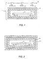
- FIG. 1 is a sectional side view of a thermal processor embodiment of the present invention.
- FIG. 2 is a view similar to that of FIG. 1 wherein a wavelength selective coating is situated on an inner chamber wall and covered by a passivation layer.
- FIGs. 3-5 are views similar to that of FIG. 1 with a double-wall chamber.
- FIG. 6 is a sectional side view of a vertical thermal processor embodiment of the present invention.
- FIG. 1 is a sectional side view of a thermal processor embodiment 1 of the present invention.
- a semiconductor wafer 10 is positioned in a reactor chamber 12 and supported by small pins 14.
- the chamber has a wavelength selective coating 16 and receives radiant energy from lamp heating elements 18 and a lamp reflector 20.
- Wafer 10 may comprise any of a number of semiconductor materials such as silicon, silicon carbide, gallium arsenide, gallium nitride, for example. If desired, these semiconductor materials can be in combination with thin insulators and/or metal layers.
- Chamber 12 may comprise a material that is sufficiently optically transparent to permit high transmission of ultraviolet light and/or visible light (light including a wavelength within the range of about 200 nanometers to about 800 nanometers). Examples of material for chamber 12 include quartz, quartz doped with alumina, alumina, and synthetic silica.
- the wafer 10 is laid horizontally inside the chamber and is supported by pins 14 comprising quartz with the device surface facing the opposite side of the chamber (the non-pin side) and the lamp heating elements.
- the positioning of the wafer in the chamber is not critical.
- the wafer can be supported in a slanted or vertical position or be supported by a quartz pedestal on the middle of the reactor chamber.
- Coating 16 can be selected from any of a number of wavelength-selective materials that reflect infrared light such as, for example, indium-tin-oxide (ITO), antimony-tin-oxide (ATO), fluorine-tin-oxide (FTO), undoped tin oxide, dichroic filters, or thin metal films such as silver, aluminum, or gold.
- Dichroic filters may be fabricated of a stack of titanium oxide and silicon dioxide layers or tantalum oxide and silicon dioxide layers, for example, and are advantageous because they can survive for a long time at high temperatures.
- the coating material is capable of transmitting light including a wavelength within the range of about 200 nanometers to about 800 nanometers.
- Drude mirror coatings comprising doped semiconductor oxides
- Drude mirror coatings have been characterized with regard to electrical, optical, and material properties as discussed in T. Gerfin and M. Gratzel, "Optical properties of tin-doped indium oxide determined by spectroscopic ellipsometry", J. Appl. Phys., Vol. 79, pp. 1722-1729, 1 Feb. 1996.
- Drude mirror coatings have been used on glass panes of greenhouses to reduce energy losses caused by emission of infrared radiation while allowing sunlight to enter freely as described in S.D. Silverstein, "Effect of Infrared Transparency on the Heat Transfer Through Windows: A Clarification of the Greenhouse Effect", Science, Vol.
- Antimony-tin-oxide (ATO) films have been deposited by chemical vapor deposition on silicon oxide layers as described in T.P. Chow, M. Ghezzo, and B.J. Baliga, "Antimony-doped tin oxide films deposited by the oxidation of tetramethyltin and trimethylantimony", J. Electrochem. Soc., pp. 1040-45, May 1982, and it is therefore expected that ATO films can be deposited on quartz.
- Dichroic filters have been used in halogen-IR parabolic aluminum reflector (PAR) lamps available from the General Electric Company, Cleveland, Ohio, to reflect infrared radiant heat from the lamp envelope while allowing the visible radiation to be transmitted outside.
- the present invention differs from such halogen-IR PAR lamps wherein the light source is inside the coated chamber because, in the present invention, the light source is situated outside the coated chamber.
- Lamp heating elements 18 may comprise ultraviolet (UV) discharge lamps such as mercury discharge lamps, metal halide visible discharge lamps, or halogen infrared incandescent lamps, for example.
- UV ultraviolet
- the wavelength range for the visible spectrum is from about 200 nanometers to about 400 nanometers
- the wavelength range for the UV spectrum is from about 400 nanometers to about 800 nanometers. Therefore, chamber 12 and coating 16 are preferably capable of passing light at a wavelength included in a range of about 200 nanometers to about 800 nanometers.
- Lamp reflector 20 may comprise a group of concave mirrors 22 placed above the lamps to efficiently reflect the back illumination of the lamps.
- Using a UV discharge lamp to process silicon wafers is expected to increase the light utilization efficiently by thirty percent or more over conventional tungsten lamp designs even without a. coating on the chamber.
- the expected increase in efficiency is due to the fact that the silicon absorption spectrum has a larger overlap with the emission spectrum of the discharge lamp.
- Using the coating to provide heat recovery is expected to improve power efficiency by about an additional sixty-five percent. An overall improvement of about ninety-five percent is expected.
- FIG. 2 is a view similar to that of FIG. 1 wherein a wavelength selective coating 16a is situated on the inner side of chamber wall 12a and covered by a passivation layer 24.
- a wavelength selective coating 16a is situated on the inner side of chamber wall 12a and covered by a passivation layer 24.
- the coating in this embodiment should be a refractory material that does not shed any particles onto the wafer and is free of contaminants.
- Passivation layer 24 may comprise a material such as, for example, silicon oxide (SiO 2 ) having a thickness in the range of about 0.1 microns to about 0.2 microns and can be added to coating 16a of FIG. 2 or coating 16 of FIG. 1 to protect the coating.
- FIGs. 3-5 are views similar to that of FIG. 1 with a double-wall chamber for gas cooling which is useful if a single wall would result in the chamber wall temperature exceeding the thermal capability of the coating. This is useful because silicon wafers, for example, can reach temperatures exceeding 1000 °C.
- the coatings 16b and 16c, respectively are positioned between chamber walls 12b and 26, and 12c and 26c, respectively. Forced air 28 and 28c can be pumped between chamber walls.
- coating 16b is situated on an outer surface of chamber wall 12b
- coating 16c is situated on an inner surface of chamber wall 28c.
- chamber walls 12d and 26d have forced air 28d pumped therebetween and coating 16d is present on an inner surface of chamber wall 12d.
- FIG. 5 illustrates a plurality of wafers 10a and 10b in a single chamber 12d.
- FIG. 6 is a sectional side view of a vertical thermal processor embodiment 2 of the present invention wherein chamber 612 is coated with wavelength selective coating 616 and encloses a plurality of wafers 610 which can be stacked using quartz pins (not shown), for example.
- the chamber is sealed by cap 630 which may comprise a material such as quartz, for example.
- Gases such as N 2 , O 2 , or pyrogenic-generated steam can be supplied through gas inlet port 632 and released through gas outlet port 634. Radiant energy is supplied by lamp heating elements 618 of lamp assemblies 619.
Applications Claiming Priority (2)
| Application Number | Priority Date | Filing Date | Title |
|---|---|---|---|
| US08/743,587 US6067931A (en) | 1996-11-04 | 1996-11-04 | Thermal processor for semiconductor wafers |
| US743587 | 1996-11-04 |
Publications (2)
| Publication Number | Publication Date |
|---|---|
| EP0840359A2 true EP0840359A2 (de) | 1998-05-06 |
| EP0840359A3 EP0840359A3 (de) | 2002-04-03 |
Family
ID=24989354
Family Applications (1)
| Application Number | Title | Priority Date | Filing Date |
|---|---|---|---|
| EP97308821A Withdrawn EP0840359A3 (de) | 1996-11-04 | 1997-11-04 | Anlage zur thermischen Behandlung von Halbleiterscheiben |
Country Status (9)
| Country | Link |
|---|---|
| US (1) | US6067931A (de) |
| EP (1) | EP0840359A3 (de) |
| JP (1) | JPH10256171A (de) |
| KR (1) | KR19980041866A (de) |
| CA (1) | CA2216464A1 (de) |
| IL (1) | IL122034A (de) |
| RU (1) | RU2185682C2 (de) |
| SG (1) | SG55398A1 (de) |
| TW (1) | TW457594B (de) |
Cited By (4)
| Publication number | Priority date | Publication date | Assignee | Title |
|---|---|---|---|---|
| DE10051125A1 (de) * | 2000-10-16 | 2002-05-02 | Steag Rtp Systems Gmbh | Vorrichtung zum thermischen Behandeln von Substraten |
| US7094656B2 (en) * | 2003-10-07 | 2006-08-22 | Industrial Technology Research Institute | Method of forming poly-silicon thin film transistors |
| DE102005038672A1 (de) * | 2005-08-16 | 2007-02-22 | Mattson Thermal Products Gmbh | Vorrichtung zum thermischen Behandeln von Halbleitersubstraten |
| DE10297788B4 (de) * | 2002-09-09 | 2008-06-26 | Electronics And Telecommunications Research Institute | Vorrichtung für die Herstellung einer Halbleitervorrichtung mit zwei Kammern und Verfahren für die Herstellung einer Halbleitervorrichtung unter Verwendung dieser Vorrichtung |
Families Citing this family (19)
| Publication number | Priority date | Publication date | Assignee | Title |
|---|---|---|---|---|
| US6291868B1 (en) | 1998-02-26 | 2001-09-18 | Micron Technology, Inc. | Forming a conductive structure in a semiconductor device |
| US6666924B1 (en) * | 2000-03-28 | 2003-12-23 | Asm America | Reaction chamber with decreased wall deposition |
| DE10045264A1 (de) * | 2000-09-13 | 2002-03-21 | Zeiss Carl | Verfahren zum Aufheizen eines Werkstückes, insbesondere eines optischen Elementes |
| US6902622B2 (en) * | 2001-04-12 | 2005-06-07 | Mattson Technology, Inc. | Systems and methods for epitaxially depositing films on a semiconductor substrate |
| US6600138B2 (en) | 2001-04-17 | 2003-07-29 | Mattson Technology, Inc. | Rapid thermal processing system for integrated circuits |
| US6707011B2 (en) | 2001-04-17 | 2004-03-16 | Mattson Technology, Inc. | Rapid thermal processing system for integrated circuits |
| US6815241B2 (en) * | 2002-09-25 | 2004-11-09 | Cao Group, Inc. | GaN structures having low dislocation density and methods of manufacture |
| KR20040042238A (ko) * | 2002-11-13 | 2004-05-20 | 주식회사 실트론 | 실리콘 웨이퍼의 산화막 형성 장치 및 실리콘 웨이퍼의산화막 형성 방법 |
| US7115837B2 (en) * | 2003-07-28 | 2006-10-03 | Mattson Technology, Inc. | Selective reflectivity process chamber with customized wavelength response and method |
| US7037612B2 (en) * | 2003-11-26 | 2006-05-02 | Utc Fuel Cells, Llc | Moisture stabilization for a fuel cell power plant system |
| DE102004038233A1 (de) * | 2004-08-05 | 2006-03-16 | Schott Ag | Solarabsorber |
| JP4852852B2 (ja) * | 2005-02-17 | 2012-01-11 | ウシオ電機株式会社 | 加熱ユニット |
| US20070148367A1 (en) * | 2005-12-22 | 2007-06-28 | Lewis Daniel J | Chemical vapor deposition apparatus and methods of using the apparatus |
| TWI464292B (zh) * | 2008-03-26 | 2014-12-11 | Gtat Corp | 塗覆金之多晶矽反應器系統和方法 |
| US20120237695A1 (en) * | 2009-12-23 | 2012-09-20 | 2-Pye Solar, LLC | Method and apparatus for depositing a thin film |
| US20120244684A1 (en) * | 2011-03-24 | 2012-09-27 | Kunihiko Suzuki | Film-forming apparatus and method |
| US11015244B2 (en) | 2013-12-30 | 2021-05-25 | Advanced Material Solutions, Llc | Radiation shielding for a CVD reactor |
| US20160379854A1 (en) * | 2015-06-29 | 2016-12-29 | Varian Semiconductor Equipment Associates, Inc. | Vacuum Compatible LED Substrate Heater |
| FR3044023B1 (fr) * | 2015-11-19 | 2017-12-22 | Herakles | Dispositif pour le revetement d'un ou plusieurs fils par un procede de depot en phase vapeur |
Citations (6)
| Publication number | Priority date | Publication date | Assignee | Title |
|---|---|---|---|---|
| US4496609A (en) * | 1969-10-15 | 1985-01-29 | Applied Materials, Inc. | Chemical vapor deposition coating process employing radiant heat and a susceptor |
| JPS6074425A (ja) * | 1983-09-29 | 1985-04-26 | Nec Corp | 基板加熱装置 |
| US4579080A (en) * | 1983-12-09 | 1986-04-01 | Applied Materials, Inc. | Induction heated reactor system for chemical vapor deposition |
| JPS61129834A (ja) * | 1984-11-28 | 1986-06-17 | Dainippon Screen Mfg Co Ltd | 光照射型熱処理装置 |
| US4653428A (en) * | 1985-05-10 | 1987-03-31 | General Electric Company | Selective chemical vapor deposition apparatus |
| DE4026728A1 (de) * | 1990-08-24 | 1992-02-27 | Dornier Gmbh | Spektralselektive verglasung |
Family Cites Families (17)
| Publication number | Priority date | Publication date | Assignee | Title |
|---|---|---|---|---|
| US3372672A (en) * | 1966-03-21 | 1968-03-12 | Gen Electric | Photopolymerization means in a vapor deposition coating apparatus |
| DE1924997A1 (de) * | 1969-05-16 | 1970-11-19 | Siemens Ag | Vorrichtung zum epitaktischen Abscheiden von Halbleitermaterial |
| US4160929A (en) * | 1977-03-25 | 1979-07-10 | Duro-Test Corporation | Incandescent light source with transparent heat mirror |
| US4409512A (en) * | 1979-06-05 | 1983-10-11 | Duro-Test Corporation | Incandescent electric lamp with etalon type transparent heat mirror |
| US4435445A (en) * | 1982-05-13 | 1984-03-06 | Energy Conversion Devices, Inc. | Photo-assisted CVD |
| JPS5994829A (ja) * | 1982-11-22 | 1984-05-31 | Nec Corp | 半導体装置の製造方法 |
| JPS611017A (ja) * | 1984-06-13 | 1986-01-07 | Kokusai Electric Co Ltd | 半導体基板の熱処理装置 |
| US4654509A (en) * | 1985-10-07 | 1987-03-31 | Epsilon Limited Partnership | Method and apparatus for substrate heating in an axially symmetric epitaxial deposition apparatus |
| US4938815A (en) * | 1986-10-15 | 1990-07-03 | Advantage Production Technology, Inc. | Semiconductor substrate heater and reactor process and apparatus |
| JPH0474859A (ja) * | 1990-07-18 | 1992-03-10 | Shibuya Kogyo Co Ltd | 熱処理装置の加熱装置 |
| JPH0729844A (ja) * | 1993-07-14 | 1995-01-31 | Fujitsu Ltd | 半導体基板の赤外線加熱方法及び赤外線加熱装置 |
| JPH07245374A (ja) * | 1994-03-03 | 1995-09-19 | Mitsui High Tec Inc | リ−ドフレ−ム及び半導体装置 |
| US5433791A (en) * | 1994-05-26 | 1995-07-18 | Hughes Aircraft Company | MBE apparatus with photo-cracker cell |
| JPH0897167A (ja) * | 1994-09-28 | 1996-04-12 | Tokyo Electron Ltd | 処理装置及び熱処理装置 |
| US5715361A (en) * | 1995-04-13 | 1998-02-03 | Cvc Products, Inc. | Rapid thermal processing high-performance multizone illuminator for wafer backside heating |
| US5636320A (en) * | 1995-05-26 | 1997-06-03 | International Business Machines Corporation | Sealed chamber with heating lamps provided within transparent tubes |
| US5781693A (en) * | 1996-07-24 | 1998-07-14 | Applied Materials, Inc. | Gas introduction showerhead for an RTP chamber with upper and lower transparent plates and gas flow therebetween |
-
1996
- 1996-11-04 US US08/743,587 patent/US6067931A/en not_active Expired - Fee Related
-
1997
- 1997-08-30 KR KR1019970045103A patent/KR19980041866A/ko not_active Application Discontinuation
- 1997-09-25 CA CA002216464A patent/CA2216464A1/en not_active Abandoned
- 1997-10-03 TW TW086114413A patent/TW457594B/zh not_active IP Right Cessation
- 1997-10-23 SG SG1997003852A patent/SG55398A1/en unknown
- 1997-10-27 IL IL12203497A patent/IL122034A/en not_active IP Right Cessation
- 1997-10-30 JP JP9297616A patent/JPH10256171A/ja not_active Withdrawn
- 1997-11-03 RU RU97118326/28A patent/RU2185682C2/ru not_active IP Right Cessation
- 1997-11-04 EP EP97308821A patent/EP0840359A3/de not_active Withdrawn
Patent Citations (6)
| Publication number | Priority date | Publication date | Assignee | Title |
|---|---|---|---|---|
| US4496609A (en) * | 1969-10-15 | 1985-01-29 | Applied Materials, Inc. | Chemical vapor deposition coating process employing radiant heat and a susceptor |
| JPS6074425A (ja) * | 1983-09-29 | 1985-04-26 | Nec Corp | 基板加熱装置 |
| US4579080A (en) * | 1983-12-09 | 1986-04-01 | Applied Materials, Inc. | Induction heated reactor system for chemical vapor deposition |
| JPS61129834A (ja) * | 1984-11-28 | 1986-06-17 | Dainippon Screen Mfg Co Ltd | 光照射型熱処理装置 |
| US4653428A (en) * | 1985-05-10 | 1987-03-31 | General Electric Company | Selective chemical vapor deposition apparatus |
| DE4026728A1 (de) * | 1990-08-24 | 1992-02-27 | Dornier Gmbh | Spektralselektive verglasung |
Non-Patent Citations (2)
| Title |
|---|
| PATENT ABSTRACTS OF JAPAN vol. 009, no. 212 (E-339), 29 August 1985 (1985-08-29) & JP 60 074425 A (NIPPON DENKI KK), 26 April 1985 (1985-04-26) * |
| PATENT ABSTRACTS OF JAPAN vol. 010, no. 319 (E-450), 30 October 1986 (1986-10-30) & JP 61 129834 A (DAINIPPON SCREEN MFG CO LTD), 17 June 1986 (1986-06-17) * |
Cited By (6)
| Publication number | Priority date | Publication date | Assignee | Title |
|---|---|---|---|---|
| DE10051125A1 (de) * | 2000-10-16 | 2002-05-02 | Steag Rtp Systems Gmbh | Vorrichtung zum thermischen Behandeln von Substraten |
| US6965093B2 (en) | 2000-10-16 | 2005-11-15 | Mattson Thermal Products Gmbh | Device for thermally treating substrates |
| DE10297788B4 (de) * | 2002-09-09 | 2008-06-26 | Electronics And Telecommunications Research Institute | Vorrichtung für die Herstellung einer Halbleitervorrichtung mit zwei Kammern und Verfahren für die Herstellung einer Halbleitervorrichtung unter Verwendung dieser Vorrichtung |
| US7094656B2 (en) * | 2003-10-07 | 2006-08-22 | Industrial Technology Research Institute | Method of forming poly-silicon thin film transistors |
| US7361566B2 (en) | 2003-10-07 | 2008-04-22 | Industrial Technology Research Institute | Method of forming poly-silicon thin film transistors |
| DE102005038672A1 (de) * | 2005-08-16 | 2007-02-22 | Mattson Thermal Products Gmbh | Vorrichtung zum thermischen Behandeln von Halbleitersubstraten |
Also Published As
| Publication number | Publication date |
|---|---|
| CA2216464A1 (en) | 1998-05-04 |
| MX9708509A (es) | 1998-05-31 |
| RU2185682C2 (ru) | 2002-07-20 |
| TW457594B (en) | 2001-10-01 |
| KR19980041866A (ko) | 1998-08-17 |
| SG55398A1 (en) | 1998-12-21 |
| JPH10256171A (ja) | 1998-09-25 |
| US6067931A (en) | 2000-05-30 |
| IL122034A (en) | 2001-05-20 |
| EP0840359A3 (de) | 2002-04-03 |
| IL122034A0 (en) | 1998-03-10 |
Similar Documents
| Publication | Publication Date | Title |
|---|---|---|
| US6067931A (en) | Thermal processor for semiconductor wafers | |
| EP2257973B1 (de) | Silberreflektoren für halbleiterbearbeitungskammern | |
| KR101767068B1 (ko) | 기판 가열 및 냉각의 개선된 제어를 위한 장치 및 방법 | |
| KR101624217B1 (ko) | 고온계용 열 공급원 반사 필터를 포함하는 장치 | |
| CN103109359B (zh) | 用于快速热处理腔室的透明反射板 | |
| US8367983B2 (en) | Apparatus including heating source reflective filter for pyrometry | |
| JP2002203804A (ja) | 加熱装置、当該加熱装置を有する熱処理装置、及び、熱処理制御方法 | |
| CN107731718A (zh) | 用于热处理腔室的支撑圆柱 | |
| RU97118326A (ru) | Устройство термообработки полупроводниковых пластин | |
| US4311907A (en) | Radiation detector having refractive index matching means | |
| US8436519B2 (en) | Incandescent lamp incorporating infrared-reflective coating system, and lighting fixture incorporating such a lamp | |
| TWI632355B (zh) | 用於熱處理腔室中的設備及用於處理基板的系統 | |
| US20100219355A1 (en) | Apparatus for an Irradiation Unit | |
| KR20060004683A (ko) | 적외선 방출체 및 조사 장치 | |
| CN1188823A (zh) | 半导体圆片的热处理器 | |
| MXPA97008509A (en) | Thermal processor for semiconductor plates | |
| EP1380412A1 (de) | Wärmereflektierendes material und das material verwendende heizvorrichtung | |
| JP2008138985A (ja) | 熱遮蔽装置および炉内監視装置 | |
| JPH07283096A (ja) | 半導体基板の処理方法及び装置 | |
| WO2004003984A1 (ja) | 半導体製造装置 | |
| Lemiti et al. | Rapid thermal annealing applied to the optimization of titanium oxide arc | |
| Leroy et al. | High performance incandescent light bulb using a selective emitter and nanophotonic filters | |
| JPH0554691B2 (de) | ||
| JP2002198319A (ja) | 熱処理装置 | |
| JPH07283090A (ja) | 半導体基板の処理方法及び装置 |
Legal Events
| Date | Code | Title | Description |
|---|---|---|---|
| PUAI | Public reference made under article 153(3) epc to a published international application that has entered the european phase |
Free format text: ORIGINAL CODE: 0009012 |
|
| AK | Designated contracting states |
Kind code of ref document: A2 Designated state(s): AT BE CH DE DK ES FI FR GB GR IE IT LI LU MC NL PT SE Kind code of ref document: A2 Designated state(s): DE ES FR GB IE IT NL |
|
| PUAL | Search report despatched |
Free format text: ORIGINAL CODE: 0009013 |
|
| AK | Designated contracting states |
Kind code of ref document: A3 Designated state(s): AT BE CH DE DK ES FI FR GB GR IE IT LI LU MC NL PT SE |
|
| RIC1 | Information provided on ipc code assigned before grant |
Free format text: 7H 01L 21/00 A, 7C 23C 16/48 B, 7C 30B 25/10 B |
|
| 17P | Request for examination filed |
Effective date: 20021004 |
|
| AKX | Designation fees paid |
Free format text: DE ES FR GB IE IT NL |
|
| 17Q | First examination report despatched |
Effective date: 20021230 |
|
| STAA | Information on the status of an ep patent application or granted ep patent |
Free format text: STATUS: THE APPLICATION IS DEEMED TO BE WITHDRAWN |
|
| 18D | Application deemed to be withdrawn |
Effective date: 20030510 |