EP0822482B1 - Datenverarbeitungseinrichtung mit einem Mikroprozessor und einer zusätzlichen Recheneinheit - Google Patents
Datenverarbeitungseinrichtung mit einem Mikroprozessor und einer zusätzlichen Recheneinheit Download PDFInfo
- Publication number
- EP0822482B1 EP0822482B1 EP97202275A EP97202275A EP0822482B1 EP 0822482 B1 EP0822482 B1 EP 0822482B1 EP 97202275 A EP97202275 A EP 97202275A EP 97202275 A EP97202275 A EP 97202275A EP 0822482 B1 EP0822482 B1 EP 0822482B1
- Authority
- EP
- European Patent Office
- Prior art keywords
- registers
- microprocessor
- data
- computing unit
- data processing
- Prior art date
- Legal status (The legal status is an assumption and is not a legal conclusion. Google has not performed a legal analysis and makes no representation as to the accuracy of the status listed.)
- Expired - Lifetime
Links
Images
Classifications
-
- G—PHYSICS
- G06—COMPUTING OR CALCULATING; COUNTING
- G06F—ELECTRIC DIGITAL DATA PROCESSING
- G06F9/00—Arrangements for program control, e.g. control units
- G06F9/06—Arrangements for program control, e.g. control units using stored programs, i.e. using an internal store of processing equipment to receive or retain programs
- G06F9/30—Arrangements for executing machine instructions, e.g. instruction decode
- G06F9/30145—Instruction analysis, e.g. decoding, instruction word fields
- G06F9/30156—Special purpose encoding of instructions, e.g. Gray coding
-
- G—PHYSICS
- G06—COMPUTING OR CALCULATING; COUNTING
- G06F—ELECTRIC DIGITAL DATA PROCESSING
- G06F9/00—Arrangements for program control, e.g. control units
- G06F9/06—Arrangements for program control, e.g. control units using stored programs, i.e. using an internal store of processing equipment to receive or retain programs
- G06F9/30—Arrangements for executing machine instructions, e.g. instruction decode
- G06F9/30098—Register arrangements
- G06F9/3012—Organisation of register space, e.g. banked or distributed register file
- G06F9/30138—Extension of register space, e.g. register cache
-
- G—PHYSICS
- G06—COMPUTING OR CALCULATING; COUNTING
- G06F—ELECTRIC DIGITAL DATA PROCESSING
- G06F9/00—Arrangements for program control, e.g. control units
- G06F9/06—Arrangements for program control, e.g. control units using stored programs, i.e. using an internal store of processing equipment to receive or retain programs
- G06F9/30—Arrangements for executing machine instructions, e.g. instruction decode
- G06F9/38—Concurrent instruction execution, e.g. pipeline or look ahead
- G06F9/3885—Concurrent instruction execution, e.g. pipeline or look ahead using a plurality of independent parallel functional units
Definitions
- the invention relates to a data processing device with a Microprocessor and an additional computing unit, as well as on a portable Data carrier with such a data processing device.
- Such data processing devices in particular in a single Semiconductor chips are integrated are known in principle, for example from Philips' P83C852 integrated circuit data sheet.
- This integrated circuit is preferably in the form of a portable card Data carriers, e.g. with the format of a check card, built in and serve preferably for this, data according to an asymmetrical encryption method encrypt or decrypt such data.
- Data blocks are exposed with a key number modulo a constant, where the constant has a large number of digits in order to ensure the safest possible To achieve encryption.
- the necessary calculation steps can basically also be done with the microprocessor, but this would require far too long, so that an additional to the microprocessor special computing unit is integrated on the chip, which is used for encryption required calculation steps is optimally designed.
- the connection between The microprocessor and additional computing unit are made using special ones Registers that control the data transfer, as well as at least one Data storage on which both the microprocessor and additional computing unit access.
- a disadvantage of these known integrated circuits with microprocessor and additional computing unit is that after performing a Processing step or a processing cycle by the additional Computing unit the microprocessor again with new values for the register must at least partially load new operands with which the next one will be loaded Processing cycle starts. This causes a considerable loss of time, so that the entire data processing arrangement, especially with longer key numbers takes a lot of time for data encryption or decryption.
- the object of the invention is to provide a data processing device with a Specify microprocessor and an additional processing unit, in which the Computing unit after the end of a processing cycle, if possible without wasting time can immediately begin the next processing cycle for new data.
- US-A-5,121,351 relates to a data processing device which in the preamble of Claim 1 specified type and deals in principle with the mentioned task, but specifies a more complex solution for vector operations, the respective queues of the first and second registers and one Provides queue of further increment registers in a DMA controller which is initialized by the CPU.
- this object is essentially achieved in that the Register for controlling the data transmission and for command transmission as at least two sets of registers are provided.
- the outputs of this Registers are switched by the content of another register, so that only one set of registers is effective at a time.
- new data can be written in by the microprocessor at any time that this data is available when the computing unit has a processing cycle finished and immediately started the next processing cycle can be. This will result in an encryption or decryption process significantly accelerated.
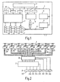
- the data processing arrangement 1 contains a microprocessor 2 as well a special computing unit 3 for certain calculations, the implementation of which Using the microprocessor 2 would be too time-consuming.
- the Microprocessor 2 is with memories 5 and 6 essentially directly over a internal bus 7 coupled and also via address register 11 with the volatile memory 4 and via further registers 10 with the computing unit 3 the registers 10 are essentially control signals for controlling the function the computing unit 3 and for controlling the transmission of operands for the and the result from the computing unit 3.
- the internal bus 13 serves essentially only for transmission of data. Since the arithmetic unit 3 also operations with long operands data bus 13 is for a larger one Data width designed, e.g. for 4 bytes. It is assumed that the Memory 5 can also deliver 4 bytes in parallel, either by appropriate Structure or through an internal series parallel implementation that contains several words from one byte in length and outputs in parallel. A corresponding The arrangement is with the register 12 at the output of the non-volatile memory 4 indicated, that is four bytes fed in succession in parallel via the bus 13 forwards. Registers 14 through 17 are designed to have 4 bytes in parallel record and parallel or possibly in smaller sections of less output as 4 bytes, depending on the word length of the computing unit 3 can process. The register 17 for the calculation results can also corresponding to the structure of the computing unit 3 several bytes in succession or record in parallel and transmit 4 bytes each in parallel via the internal bus 13.
- the control of the computing unit 3 by the registers 10 shown schematically in Fig. 1 is indicated somewhat more clearly in Fig. 2.
- a total of three sets of eight registers 201 to 271, 202 to 272 and 203 to 273 are used.
- the Outputs of all registers lead to a selection circuit 29 which outputs the selects one of these sets of registers and feeds them to the computing unit 3, whereby the selection is controlled by bit positions 310 to 312 of a further register 31.
- This register 31 is only available once.
- the inputs of all registers are on the internal data bus 7 connected and can be used individually by the microprocessor be selected for writing, the selection lines of Are omitted for the sake of clarity.
- Registers 201 through 271, 202 through 272 and 203 to 273 can only receive one byte of data from the internal bus 7 and only output to the selection circuit 29, while the register 31 bit by bit is writable and readable, the bit positions 310 to 313 only from the internal Take over data bus data and the selection circuit 29 and via the outputs control the arithmetic unit 3, while the bit positions 314 to 317 for further Communication between the computing unit 3 and the microprocessor are provided.
- the eight registers that are in each set of registers serve the following purposes, with reference to the registers of only the first set for simplicity.
- the register 201 contains the operation code for controlling the computing unit 3 and information from which the memory 5 or 6 operands are taken.
- Register 211 specifies the start address for the first operand.
- Register 221 contains the start address for the second operand.
- the register 231 contains the address for a further operand which, depending on the operation to be carried out with the computing unit 3, in different Way is processed in the computing unit. For example, the operand specified by this address represents the module in modulo operations.
- Register 241 contains an address for the computation result of arithmetic unit 3.
- Registers 251 and 261 are used to specify the length of the first operand and the second operand, respectively.
- the register 271 finally contains part of an address for the non-volatile memory 4, it being assumed that this memory has more memory locations than can be addressed with a byte.
- the computing power of the arithmetic unit 3 can be optimally used, since during the execution of a calculation under Using a set of registers, for example 201 to 271, the Microprocessor can load the registers of a further set, for example registers 202 to 272, with new values, and if the computing unit 3 a set Operands completely processed and the result delivered, the Microprocessor change the contents of bit positions 310 to 312 of register 31 in one step, so that the addresses for new operands become immediately valid and the calculation with these operands can start without waiting. Specifying the operand addresses using the start address and operand length enables the operands to be addressed very easily, quickly and in a register-saving manner.
Landscapes
- Engineering & Computer Science (AREA)
- Software Systems (AREA)
- Theoretical Computer Science (AREA)
- Physics & Mathematics (AREA)
- General Engineering & Computer Science (AREA)
- General Physics & Mathematics (AREA)
- Advance Control (AREA)
- Executing Machine-Instructions (AREA)
- Microcomputers (AREA)
- Multi Processors (AREA)
Applications Claiming Priority (2)
| Application Number | Priority Date | Filing Date | Title |
|---|---|---|---|
| DE19630861A DE19630861A1 (de) | 1996-07-31 | 1996-07-31 | Datenverarbeitungseinrichtung mit einem Mikroprozessor und einer zusätzlichen Recheneinheit |
| DE19630861 | 1996-07-31 |
Publications (3)
| Publication Number | Publication Date |
|---|---|
| EP0822482A2 EP0822482A2 (de) | 1998-02-04 |
| EP0822482A3 EP0822482A3 (de) | 1998-09-23 |
| EP0822482B1 true EP0822482B1 (de) | 2003-07-16 |
Family
ID=7801351
Family Applications (1)
| Application Number | Title | Priority Date | Filing Date |
|---|---|---|---|
| EP97202275A Expired - Lifetime EP0822482B1 (de) | 1996-07-31 | 1997-07-21 | Datenverarbeitungseinrichtung mit einem Mikroprozessor und einer zusätzlichen Recheneinheit |
Country Status (4)
| Country | Link |
|---|---|
| US (1) | US5889622A (enExample) |
| EP (1) | EP0822482B1 (enExample) |
| JP (1) | JPH1091593A (enExample) |
| DE (2) | DE19630861A1 (enExample) |
Families Citing this family (5)
| Publication number | Priority date | Publication date | Assignee | Title |
|---|---|---|---|---|
| US6901491B2 (en) * | 2001-10-22 | 2005-05-31 | Sun Microsystems, Inc. | Method and apparatus for integration of communication links with a remote direct memory access protocol |
| JP3904432B2 (ja) | 2001-11-16 | 2007-04-11 | 株式会社ルネサステクノロジ | 情報処理装置 |
| DE10256586A1 (de) * | 2002-12-04 | 2004-06-17 | Philips Intellectual Property & Standards Gmbh | Datenverarbeitungseinrichtung mit Mikroprozessor und mit zusätzlicher Recheneinheit sowie zugeordnetes Verfahren |
| US20050141095A1 (en) * | 2003-12-29 | 2005-06-30 | Youngtack Shim | Reflecting sheet |
| JP4591279B2 (ja) * | 2005-08-19 | 2010-12-01 | ソニー株式会社 | 情報処理装置および情報処理方法、記録媒体、並びに、プログラム |
Family Cites Families (9)
| Publication number | Priority date | Publication date | Assignee | Title |
|---|---|---|---|---|
| US3617720A (en) * | 1967-09-12 | 1971-11-02 | Bell Telephone Labor Inc | Fast fourier transform using hierarchical store |
| JPS6297062A (ja) * | 1985-10-23 | 1987-05-06 | Mitsubishi Electric Corp | デイジタルシグナルプロセツサ |
| IL81762A0 (en) * | 1986-04-11 | 1987-10-20 | Symbolics Inc | Instruction prefetch unit |
| US4969121A (en) * | 1987-03-02 | 1990-11-06 | Altera Corporation | Programmable integrated circuit logic array device having improved microprocessor connectability |
| JPH0719204B2 (ja) * | 1987-09-17 | 1995-03-06 | 筑波大学長 | 浮動小数点演算方式 |
| FR2656710A1 (fr) * | 1989-12-29 | 1991-07-05 | Radiotechnique Compelec | Microcontroleur pour l'execution rapide d'un grand nombre d'operations decomposable en sequence d'operations de meme nature. |
| JP2513139B2 (ja) * | 1993-07-27 | 1996-07-03 | 日本電気株式会社 | 信号処理プロセッサ |
| US5604909A (en) * | 1993-12-15 | 1997-02-18 | Silicon Graphics Computer Systems, Inc. | Apparatus for processing instructions in a computing system |
| US5732251A (en) * | 1996-05-06 | 1998-03-24 | Advanced Micro Devices | DSP with register file and multi-function instruction sequencer for vector processing by MACU |
-
1996
- 1996-07-31 DE DE19630861A patent/DE19630861A1/de not_active Withdrawn
-
1997
- 1997-07-21 EP EP97202275A patent/EP0822482B1/de not_active Expired - Lifetime
- 1997-07-21 DE DE59710434T patent/DE59710434D1/de not_active Expired - Lifetime
- 1997-07-28 JP JP9201287A patent/JPH1091593A/ja active Pending
- 1997-07-31 US US08/903,566 patent/US5889622A/en not_active Expired - Fee Related
Also Published As
| Publication number | Publication date |
|---|---|
| DE19630861A1 (de) | 1998-02-05 |
| US5889622A (en) | 1999-03-30 |
| DE59710434D1 (de) | 2003-08-21 |
| EP0822482A2 (de) | 1998-02-04 |
| JPH1091593A (ja) | 1998-04-10 |
| EP0822482A3 (de) | 1998-09-23 |
Similar Documents
| Publication | Publication Date | Title |
|---|---|---|
| DE2755273C2 (enExample) | ||
| DE3807997C2 (enExample) | ||
| DE4035405C2 (enExample) | ||
| DE2545873A1 (de) | Zugriffsfolgesteuervorrichtung fuer eine speichereinheit | |
| DE2145120A1 (de) | Digitales Datenverarbeitungsgerat | |
| DE2713648A1 (de) | Stromzufuhr-steuervorrichtung fuer speichervorrichtungen | |
| DE69119149T2 (de) | Struktur zur direkten Speicher-zu-Speicher-Übertragung | |
| DE3841370A1 (de) | Verfahren und vorrichtung fuer eine crc-berechnung | |
| DE3043653A1 (de) | Datenverarbeitungsanlage | |
| DE3716752C2 (enExample) | ||
| DE3338329C2 (enExample) | ||
| EP0822482B1 (de) | Datenverarbeitungseinrichtung mit einem Mikroprozessor und einer zusätzlichen Recheneinheit | |
| DE3811145A1 (de) | Vorrichtung zum verarbeiten von bildern mit gewuenschten grauwerten | |
| DE3506592C2 (de) | Aufzeichnungsgerät | |
| DE3107568A1 (de) | Datenverarbeitungseinrichtung | |
| DE1499191B2 (de) | Elektronische einrichtung fuer eine datenverarbeitungsanlage | |
| DE2747304C3 (de) | Einrichtung zur Mikrobefehlssteuerung | |
| DE10105627B4 (de) | Mehrfachanschlussspeichereinrichtung, Verfahren und System zum Betrieb einer Mehrfachanschlussspeichereinrichtung | |
| DE1296429B (de) | Datenbearbeitungsanlage | |
| DE1524211A1 (de) | Datenverarbeitungsanlage | |
| EP1393164B1 (de) | Prozessor mit interner speicherkonfiguration und anordnung mit diesem prozessor | |
| DE3326898C2 (de) | Datenverarbeitungsmaschine | |
| DE10256586A1 (de) | Datenverarbeitungseinrichtung mit Mikroprozessor und mit zusätzlicher Recheneinheit sowie zugeordnetes Verfahren | |
| WO2004042740A1 (de) | Verfahren zum betreiben einer speicheranordnung | |
| DE69516817T2 (de) | Peripheriegerät zur Ausführung von Bitfeldbefehlen |
Legal Events
| Date | Code | Title | Description |
|---|---|---|---|
| PUAI | Public reference made under article 153(3) epc to a published international application that has entered the european phase |
Free format text: ORIGINAL CODE: 0009012 |
|
| AK | Designated contracting states |
Kind code of ref document: A2 Designated state(s): DE FR GB IT |
|
| AX | Request for extension of the european patent |
Free format text: AL;LT;LV;RO;SI |
|
| PUAL | Search report despatched |
Free format text: ORIGINAL CODE: 0009013 |
|
| RAP3 | Party data changed (applicant data changed or rights of an application transferred) |
Owner name: KONINKLIJKE PHILIPS ELECTRONICS N.V. Owner name: PHILIPS PATENTVERWALTUNG GMBH |
|
| AK | Designated contracting states |
Kind code of ref document: A3 Designated state(s): AT BE CH DE DK ES FI FR GB GR IE IT LI LU MC NL PT SE |
|
| AX | Request for extension of the european patent |
Free format text: AL;LT;LV;RO;SI |
|
| 17P | Request for examination filed |
Effective date: 19990323 |
|
| AKX | Designation fees paid |
Free format text: DE FR GB IT |
|
| RBV | Designated contracting states (corrected) |
Designated state(s): DE FR GB IT |
|
| RAP3 | Party data changed (applicant data changed or rights of an application transferred) |
Owner name: KONINKLIJKE PHILIPS ELECTRONICS N.V. Owner name: PHILIPS CORPORATE INTELLECTUAL PROPERTY GMBH |
|
| RAP1 | Party data changed (applicant data changed or rights of an application transferred) |
Owner name: KONINKLIJKE PHILIPS ELECTRONICS N.V. Owner name: PHILIPS CORPORATE INTELLECTUAL PROPERTY GMBH |
|
| GRAH | Despatch of communication of intention to grant a patent |
Free format text: ORIGINAL CODE: EPIDOS IGRA |
|
| RIC1 | Information provided on ipc code assigned before grant |
Free format text: 7G 06F 9/318 A, 7G 06F 9/38 B |
|
| RAP1 | Party data changed (applicant data changed or rights of an application transferred) |
Owner name: KONINKLIJKE PHILIPS ELECTRONICS N.V. Owner name: PHILIPS INTELLECTUAL PROPERTY & STANDARDS GMBH |
|
| GRAH | Despatch of communication of intention to grant a patent |
Free format text: ORIGINAL CODE: EPIDOS IGRA |
|
| GRAA | (expected) grant |
Free format text: ORIGINAL CODE: 0009210 |
|
| AK | Designated contracting states |
Designated state(s): DE FR GB IT |
|
| PG25 | Lapsed in a contracting state [announced via postgrant information from national office to epo] |
Ref country code: IT Free format text: LAPSE BECAUSE OF FAILURE TO SUBMIT A TRANSLATION OF THE DESCRIPTION OR TO PAY THE FEE WITHIN THE PRESCRIBED TIME-LIMIT;WARNING: LAPSES OF ITALIAN PATENTS WITH EFFECTIVE DATE BEFORE 2007 MAY HAVE OCCURRED AT ANY TIME BEFORE 2007. THE CORRECT EFFECTIVE DATE MAY BE DIFFERENT FROM THE ONE RECORDED. Effective date: 20030716 |
|
| REG | Reference to a national code |
Ref country code: GB Ref legal event code: FG4D Free format text: NOT ENGLISH |
|
| REF | Corresponds to: |
Ref document number: 59710434 Country of ref document: DE Date of ref document: 20030821 Kind code of ref document: P |
|
| GBT | Gb: translation of ep patent filed (gb section 77(6)(a)/1977) | ||
| REG | Reference to a national code |
Ref country code: GB Ref legal event code: 746 Effective date: 20030829 |
|
| ET | Fr: translation filed | ||
| PLBE | No opposition filed within time limit |
Free format text: ORIGINAL CODE: 0009261 |
|
| STAA | Information on the status of an ep patent application or granted ep patent |
Free format text: STATUS: NO OPPOSITION FILED WITHIN TIME LIMIT |
|
| REG | Reference to a national code |
Ref country code: FR Ref legal event code: D6 |
|
| 26N | No opposition filed |
Effective date: 20040419 |
|
| REG | Reference to a national code |
Ref country code: GB Ref legal event code: 732E |
|
| REG | Reference to a national code |
Ref country code: FR Ref legal event code: TP |
|
| REG | Reference to a national code |
Ref country code: FR Ref legal event code: PLFP Year of fee payment: 20 |
|
| PGFP | Annual fee paid to national office [announced via postgrant information from national office to epo] |
Ref country code: GB Payment date: 20160627 Year of fee payment: 20 |
|
| PGFP | Annual fee paid to national office [announced via postgrant information from national office to epo] |
Ref country code: FR Payment date: 20160622 Year of fee payment: 20 |
|
| PGFP | Annual fee paid to national office [announced via postgrant information from national office to epo] |
Ref country code: DE Payment date: 20160622 Year of fee payment: 20 |
|
| REG | Reference to a national code |
Ref country code: DE Ref legal event code: R071 Ref document number: 59710434 Country of ref document: DE |
|
| REG | Reference to a national code |
Ref country code: GB Ref legal event code: PE20 Expiry date: 20170720 |
|
| PG25 | Lapsed in a contracting state [announced via postgrant information from national office to epo] |
Ref country code: GB Free format text: LAPSE BECAUSE OF EXPIRATION OF PROTECTION Effective date: 20170720 |