EP0817199B1 - Améliorations à des circuits électroniques - Google Patents
Améliorations à des circuits électroniques Download PDFInfo
- Publication number
- EP0817199B1 EP0817199B1 EP97110765A EP97110765A EP0817199B1 EP 0817199 B1 EP0817199 B1 EP 0817199B1 EP 97110765 A EP97110765 A EP 97110765A EP 97110765 A EP97110765 A EP 97110765A EP 0817199 B1 EP0817199 B1 EP 0817199B1
- Authority
- EP
- European Patent Office
- Prior art keywords
- coupled
- cell
- rtds
- negative resistance
- memory system
- Prior art date
- Legal status (The legal status is an assumption and is not a legal conclusion. Google has not performed a legal analysis and makes no representation as to the accuracy of the status listed.)
- Expired - Lifetime
Links
Images


Classifications
-
- B—PERFORMING OPERATIONS; TRANSPORTING
- B82—NANOTECHNOLOGY
- B82Y—SPECIFIC USES OR APPLICATIONS OF NANOSTRUCTURES; MEASUREMENT OR ANALYSIS OF NANOSTRUCTURES; MANUFACTURE OR TREATMENT OF NANOSTRUCTURES
- B82Y10/00—Nanotechnology for information processing, storage or transmission, e.g. quantum computing or single electron logic
-
- G—PHYSICS
- G11—INFORMATION STORAGE
- G11C—STATIC STORES
- G11C11/00—Digital stores characterised by the use of particular electric or magnetic storage elements; Storage elements therefor
-
- G—PHYSICS
- G11—INFORMATION STORAGE
- G11C—STATIC STORES
- G11C11/00—Digital stores characterised by the use of particular electric or magnetic storage elements; Storage elements therefor
- G11C11/21—Digital stores characterised by the use of particular electric or magnetic storage elements; Storage elements therefor using electric elements
- G11C11/34—Digital stores characterised by the use of particular electric or magnetic storage elements; Storage elements therefor using electric elements using semiconductor devices
- G11C11/36—Digital stores characterised by the use of particular electric or magnetic storage elements; Storage elements therefor using electric elements using semiconductor devices using diodes, e.g. as threshold elements, i.e. diodes assuming a stable ON-stage when driven above their threshold (S- or N-characteristic)
-
- G—PHYSICS
- G11—INFORMATION STORAGE
- G11C—STATIC STORES
- G11C2211/00—Indexing scheme relating to digital stores characterized by the use of particular electric or magnetic storage elements; Storage elements therefor
- G11C2211/56—Indexing scheme relating to G11C11/56 and sub-groups for features not covered by these groups
- G11C2211/561—Multilevel memory cell aspects
- G11C2211/5614—Multilevel memory cell comprising negative resistance, quantum tunneling or resonance tunneling elements
Definitions
- the present invention relates generally to electronic circuits and, more particularly, to memory cells having negative differential resistance devices such as resonant tunneling diodes.
- High density integrated semiconductor random access memory is reaching the gigabit scale, led by the progressive evolutionary development of dynamic RAM (DRAM).
- DRAM dynamic RAM
- the 1T/1C DRAM cell consisting of a pass transistor and a capacitor, has the smallest possible cell size, ranging between 4F 2 and 8F 2 , where F is the minimum feature size.
- DRAM requires periodic refreshing, of the order of once per millisecond, since a bit is stored as charge on a capacitor, and the charge leaks away, at a rate of approximately 1 fA (10 -15 A) per cell.
- Static RAM provides enhanced functional qualities; no refreshing is needed and it is also generally faster than DRAM (approximately 25 nsec for SRAM compared to approximately 80 nsec for DRAM).
- DRAM approximately 25 nsec for SRAM compared to approximately 80 nsec for DRAM.
- the SRAM cell is more complex, requiring either six transistors or four transistors and two polysilicon load resistors, resulting in a cell size approximating 60 F 2 . It would be highly desirable to have memory cells with the functional qualities of SRAM, but with cell density closer to that of DRAM.
- a resonant tunneling diode in its simplest form consists of a sequence of five semiconductor layers.
- the outer two layers are the contact layers into which electrons enter and exit the semiconductor layer sequence.
- the interior three dissimilar semiconductor layers differ in their energy band gaps in the sequence wide/narrow/wide band gap with layer thicknesses comparable to the electron Bloch wavelength (typically less than 10nm).
- This sequence of layers produces an energy profile through which electrons must travel and which consists of two energy barriers separated by a narrow region referred to as a quantum well.
- the quantum well width is selected to be approximately equal to some integer or half-integer multiple of the electron wavelength, a standing wave can be built up by constructive interference analogous to the standing waves in a microwave cavity. Electrons at these wavelengths couple into and out of the quantum well more readily than others.
- the current-voltage characteristic of the resonant tunneling diode is N-shaped. It is this characteristic which is utilized to advantage in resonant tunneling electron devices.
- RTDs are often used in logic and analog signal processing circuits. They display a multistate and/or multilevel switching characteristic that is very useful in reducing the size, power dissipation or delay of conventional circuits.
- the operation of an RTD often creates a problem due to its inherent electrical hysteresis. Once switched from a low to a high voltage or current state, a reset of its applied bias is required to return the device to its original state.
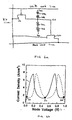
- the traditional Goto cell which is disclosed in E. Goto, IRE Trans. Electronic Computers, March 1960, at p. 25, consists of a pass transistor 10 and two RTDs 12 and 14, and is shown in FIG. 1a, has the advantage of compactness and being static.
- FIG. 1b illustrates a load line analysis of the circuit of FIG. 1a, showing the two stable latching points 16 and 18.
- the valley current causes large static power dissipation.
- the idea of a "gain stage" to amplify the action of the RTD latch pair arises.
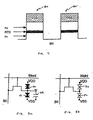
- FIGS. 2a through 2d For CMOS gigabit DRAM, a number of 2-transistor (2T) gain cells have been proposed, four of which are shown in FIGS. 2a through 2d, to reduce the required storage node capacitance.
- the circuit of FIG. 2a is disclosed in H. Shichijo et al., Ext. Abs. 16th Int. Conf. on Solid State Dev. and Mat. (1984), p. 265.
- the circuit of FIG. 2b is disclosed in W. Kim, IEEE J. Solid State Circuits, vol. 29 (1994) at p. 978.
- the circuit of FIG. 2c is disclosed in S. Shukuri, Int. Electron Dev. Meeting Tech. Digest (1992) at p. 32.8.1.
- the circuit of FIG. 2d is disclosed in M.
- the present invention is defined by claims 1 and 5. It includes a memory cell comprising a p-channel FET having its gate electrode coupled to a write word line and its drain electrode coupled to a bit line, and an n-channel FET having its source electrode coupled to the bit line and its drain electrode coupled to a read word line.
- a pair of series connected resonant tunneling diodes coupled between a supply voltage and substrate voltage have their common connection coupled to the source electrode of the p-channel FET and to the gate electrode of the n-channel FET.
- This memory cell circuit includes p-channel FET 20, n-channel FET 22, and resonant tunneling diodes (RTDs) 24 and 26.
- the circuit is configured such that p-channel FET 20 has its gate electrode coupled to a write word line and its drain electrode coupled to a bit line.
- N-channel FET 22 has its source electrode coupled to the bit line and its drain electrode coupled to a read word line.
- RTDs 24 and 26 are coupled as a series-connected pair between a supply voltage V DD and substrate voltage V SS and have their common connection coupled to the source electrode of p-channel FET 20 and to the gate electrode of n-channel FET 22 at storage node SN.
- CMOS cell similar to that taught in the Shukuri et al. reference, and shown in FIG. 2c, is assumed, thereby allowing operation at 1 volt.
- the latching operation of the pair of RTDs 24 and 26 cancels any leakage currents which might normally disturb the cell state, thereby eliminating the refresh requirement.
- the DRAM cell of the type shown in FIG. 1 is transformed into a SRAM cell by the modification of the FIG. 3 device.
- RTDs 24 and 26 can be ultra-low current density devices, as their active current needs to be only slightly larger than the leakage current of a DRAM cell of the type shown in FIG. 1. These currents are on the order of 1 fA (10 -15 A) per cell, leading to an ultra-low required RTD current density of only 10 -6 A/cm 2 . At such current levels, the RTD latch 24, 26 has a time constant in the millisecond range. Any higher current level will increase latching speed, which is not necessary, but dissipate extra power. No high peak-to-valley current ratio of RTDs 24 and 26 is required, as long as non-destructive readout (NDR) is present.
- NDR non-destructive readout
- the memory cell of FIG. 3 was simulated using SPICE, a standard computer modelling program for integrated circuit emulation.
- the simulation used standard 0.4 ⁇ m gate length silicon CMOS transistor models and Texas Instruments-developed SPICE RTD models.
- the simulation circuit is shown in FIG. 4.
- the widths of the p-channel write FET 20 and the n-channel read-FET 22 we chosen to be equal to 1 ⁇ m, and the areas of the two RTDs 24 and 26 were chosen to be equal to 0.25 ⁇ m 2 .
- the table at FIG. 4 defines the three states of the memory cell. "Standby" means that the cell will not be written to or read from even when cells on the same word line or bit line are being addressed.
- FIG. 5 shows the result of the above simulation for parameters of RTDs 24 and 26 chosen to yield 10 -4 A/cm 2 valley current density (0.25 pA/cell), shown in FIG. 5 as solid lines, and a peak-to-valley current ratio of about 8.
- the current density is increased by a factor of 1000, shown in FIG. 5 as dashed lines, some latching effects begin to be seen, even on the msec scale. This implicitly shows that an ultra-low current density pair of RTDs will make the DRAM cell of FIG. 1 stable against leakage.
- FIG. 6a illustrates a memory cell circuit in accordance with a second embodiment of the present invention, wherein three stable states are obtained by increasing the number of RTDs on each side of storage node SN from one to two, yielding a series connection of RTDs 24a, 24b, 26a and 26b.
- FIG. 6b illustrates a load line graph showing three stable points 30, 32 and 34 for the middle node SN of four series-connected RTDs in the FIG. 6a embodiment.
- FIG. 7 illustrates a view of an RTD latch structure.
- the two "legs" of the RTD stack are two mesa-shaped columns 40 and 42, and they share the same epitaxial layer structure containing one, two or more RTDs.
- This type of structure is present on storage node SN, i.e. the source electrode of write FET 20 of Fig. 3.
- RTDs have been realized in an InP-based material system with current densities on the order of only 1 A/cm 2 (and peak-to-valley ratio around 8). This is four to five orders of magnitude lower than for conventional high-speed RTDs, but still much higher than the number 10 -6 A/cm 2 which was discussed earlier as a goal.
- CMOS devices and RTDs described for use in the present invention may be integrated in a III/V semiconductor system. Direct integration seems possible only with lift-off and epitaxial placement techniques, which are currently in development at some places, but may never reach a cost level that is compatible with CMOS DRAM mass production. Another option is the possible development of ultra-low current RTDs based on silicon. Yet another option would employ ultra-low current density Esaki Type diodes based on Si or SiGe.
- FIG. 8a illustrates a cell which demonstrates some amount of similarity both to a Goto cell (FIG. 1a) and to a standard DRAM cell (one pass transistor and a capacitor, i.e. 1T/1C). Its operation is closest to that of the DRAM cell:
- the RTD pair comprising diodes 44 and 46 merely compensates for the leakage current of capacitor 48.
- the DRAM cell is transformed into an SRAM cell.
- the RTD latch 44 and 46 is again ultra-low current density (as opposed to the Goto cell of FIG. 1b), since capacitor 48 ( ⁇ 25 fF) drives the bit line during the read operation, as in conventional DRAM.
- the cell of FIG. 8a is less robust than the 2T/NDR diode cell, but has the potential of very small size (close to DRAM cell size). It will also have a lower speed, namely the same as the corresponding DRAM cell speed. Finally, the read operation will have to be performed just as in DRAM, with automatic refresh. The important difference with DRAM is that no other (periodic) refresh operation is required. A negative difference with the conventional DRAM cell is that one more bias line (VDD or VSS) must be supplied to each cell. Multi-valued data storage, while not impossible, will be much harder with this design that the 2T/NDR diode cell of FIG. 3.
- FIG. 8a Materials issues with the FIG. 8a embodiment are generally the same as for the 2T/NDR diode cell of FIG. 3, with the exception that one should realize the large capacitance 48 as a physical part of NDR diodes.
- FIG. 8b Such a device is shown in FIG. 8b, wherein negative differential resistance diodes 50 and 52 physically incorporate the needed capacitance. The following are considered important properties for the cell of FIG. 8a:
- the device of FIG. 8a may be considered either a "high capacitance NDR diode” or an “NDR leakage current capacitor.”
- Current DRAM capacitors satisfy the above properties 1 and 3 (with 75 fF/ ⁇ m 2 for Gbit cell designs), but not property 2. Realization of this "anomalous' capacitor means that existing DRAM designs could be turned into SRAM designs with only a slight hit in density and with the addition of one more bias line per cell. This would be much better than current SRAM cell architectures, except possibly for access speed.
Landscapes
- Engineering & Computer Science (AREA)
- Computer Hardware Design (AREA)
- Chemical & Material Sciences (AREA)
- Nanotechnology (AREA)
- Physics & Mathematics (AREA)
- Mathematical Physics (AREA)
- Theoretical Computer Science (AREA)
- Crystallography & Structural Chemistry (AREA)
- Static Random-Access Memory (AREA)
- Dram (AREA)
- Semiconductor Memories (AREA)
Claims (7)
- Système de mémoire organisé sous la forme d'une matrice contenant une cellule de mémoire à chaque intersection d'une ligne de bits avec des lignes de mots de lecture et d'écriture, ladite cellule de mémoire comportant :caractérisé par un second transistor (22) ayant une électrode de source raccordée à ladite ligne de bits, une électrode de drain raccordée à une ligne de mots de lecture, et une électrode de grille raccordée audit point commun.un premier transistor (20) ayant une électrode de grille raccordée à une ligne de mots d'écriture et une électrode de drain raccordée à une ligne de bits ;un premier et un second dispositifs (21, 26) à résistance négative raccordés en série entre une tension d'alimentation et une tension de substrat, le point commun desdits dispositifs à résistance négative raccordés en série étant raccordé à l'électrode de source dudit premier FET (20),
- Système de mémoire selon la revendication 1, dans lequel ledit premier transistor est un FET à canal P.
- Système de mémoire selon la revendication 1 ou 2, dans lequel le second FET est un FET à canal N.
- Système de mémoire selon l'une quelconque des revendications précédentes, dans lequel lesdits premier et second dispositifs à résistance négative sont des diodes (RTDs) à effet tunnel résonnant.
- Système de mémoire organisé sous la forme d'une matrice contenant une cellule de mémoire à chaque intersection d'une ligne de bits avec une ligne de mots, ladite cellule de mémoire comportant :un condensateur raccordé entre ledit point commun auxdits dispositifs à résistance négative raccordés en série et l'une desdites tensions d'alimentation et de substrat.un transistor ayant une électrode de grille raccordée à une ligne de mots et une électrode choisie parmi une électrode de drain ou de source raccordée à une ligne de bits ;un premier et un second dispositifs à résistance négative raccordés en série entre une tension d'alimentation et une tension de substrat, un point commun auxdits dispositifs à résistance négative raccordés en série étant raccordé à l'autre desdites électrodes de drain et de source ; caractérisé par
- Système de mémoire selon la revendication 5, dans lequel ledit transistor est un FET à canal N.
- Système de mémoire selon la revendication 5 ou la revendication 6, dans lequel lesdits premier et second dispositifs à résistance négative sont des diodes (RTDs) à effet tunnel résonnant.
Applications Claiming Priority (2)
| Application Number | Priority Date | Filing Date | Title |
|---|---|---|---|
| US2116596P | 1996-07-01 | 1996-07-01 | |
| US21165P | 1996-07-01 |
Publications (3)
| Publication Number | Publication Date |
|---|---|
| EP0817199A2 EP0817199A2 (fr) | 1998-01-07 |
| EP0817199A3 EP0817199A3 (fr) | 1999-10-13 |
| EP0817199B1 true EP0817199B1 (fr) | 2002-11-27 |
Family
ID=21802720
Family Applications (1)
| Application Number | Title | Priority Date | Filing Date |
|---|---|---|---|
| EP97110765A Expired - Lifetime EP0817199B1 (fr) | 1996-07-01 | 1997-07-01 | Améliorations à des circuits électroniques |
Country Status (6)
| Country | Link |
|---|---|
| EP (1) | EP0817199B1 (fr) |
| JP (1) | JP3884536B2 (fr) |
| KR (1) | KR100450362B1 (fr) |
| DE (1) | DE69717352T2 (fr) |
| SG (1) | SG54526A1 (fr) |
| TW (1) | TW400636B (fr) |
Families Citing this family (2)
| Publication number | Priority date | Publication date | Assignee | Title |
|---|---|---|---|---|
| JP2003051184A (ja) * | 2001-08-06 | 2003-02-21 | Nec Corp | メモリ装置 |
| US9536886B2 (en) * | 2015-03-02 | 2017-01-03 | Samsung Electronics Co., Ltd. | CMOS compatible resonant interband tunneling cell |
Family Cites Families (2)
| Publication number | Priority date | Publication date | Assignee | Title |
|---|---|---|---|---|
| JPH0661454A (ja) * | 1992-08-10 | 1994-03-04 | Hitachi Ltd | 半導体集積回路装置 |
| US5390145A (en) * | 1993-04-15 | 1995-02-14 | Fujitsu Limited | Resonance tunnel diode memory |
-
1997
- 1997-07-01 KR KR1019970030495A patent/KR100450362B1/ko not_active IP Right Cessation
- 1997-07-01 DE DE69717352T patent/DE69717352T2/de not_active Expired - Lifetime
- 1997-07-01 JP JP21111197A patent/JP3884536B2/ja not_active Expired - Fee Related
- 1997-07-01 EP EP97110765A patent/EP0817199B1/fr not_active Expired - Lifetime
- 1997-07-01 SG SG1997002334A patent/SG54526A1/en unknown
- 1997-10-06 TW TW086109356A patent/TW400636B/zh not_active IP Right Cessation
Also Published As
| Publication number | Publication date |
|---|---|
| DE69717352D1 (de) | 2003-01-09 |
| JP3884536B2 (ja) | 2007-02-21 |
| SG54526A1 (en) | 1998-11-16 |
| EP0817199A2 (fr) | 1998-01-07 |
| KR980011423A (ko) | 1998-04-30 |
| EP0817199A3 (fr) | 1999-10-13 |
| TW400636B (en) | 2000-08-01 |
| DE69717352T2 (de) | 2003-06-26 |
| JPH1069766A (ja) | 1998-03-10 |
| KR100450362B1 (ko) | 2004-11-26 |
Similar Documents
| Publication | Publication Date | Title |
|---|---|---|
| US5883829A (en) | Memory cell having negative differential resistance devices | |
| US7466586B2 (en) | Diode-based capacitor memory and its applications | |
| US5937295A (en) | Nano-structure memory device | |
| van der Wagt | Tunneling-based SRAM | |
| Terauchi et al. | A surrounding gate transistor (SGT) gain cell for ultra high density DRAMs | |
| US5448513A (en) | Capacitorless DRAM device on silicon-on-insulator substrate | |
| JP5542369B2 (ja) | いくつかのレベルのところに集積された、しきい値電圧vtが動的に調整可能なトランジスタを有するsramメモリセル | |
| JP2915011B2 (ja) | 単発性乱調の防護のための容量性を有したメモリ・セル | |
| US20090303801A1 (en) | Carbon nanotube memory including a buffered data path | |
| JP2005514775A (ja) | 微分負性抵抗電界効果トランジスタを用いたメモリセル | |
| US7675768B1 (en) | Low power carbon nanotube memory | |
| US5677637A (en) | Logic device using single electron coulomb blockade techniques | |
| EP0048814A2 (fr) | Cellule de mémoire non volatile semiconductrice | |
| US7187028B2 (en) | Silicon on insulator (SOI) negative differential resistance (NDR) based memory device with reduced body effects | |
| US6038163A (en) | Capacitor loaded memory cell | |
| Durrani et al. | Coulomb blockade memory using integrated Single-Electron Transistor/Metal-Oxide-Semiconductor transistor gain cells | |
| EP0674798B1 (fr) | Dispositif a memoire | |
| Lee et al. | Low-voltage, high-speed circuit designs for gigabit DRAMs | |
| US6490193B1 (en) | Forming and storing data in a memory cell | |
| EP0817199B1 (fr) | Améliorations à des circuits électroniques | |
| US5640341A (en) | Memory cell insensitive to collisions of heavy ions | |
| US4788662A (en) | Semiconductor memory device using resonant-tunneling hot electron transistor | |
| US6621727B2 (en) | Three-transistor SRAM device | |
| Uemura et al. | Design and analysis of resonant-tunneling-diode (RTD) based high performance memory system | |
| US5886921A (en) | Static random access memory cell having graded channel metal oxide semiconductor transistors and method of operation |
Legal Events
| Date | Code | Title | Description |
|---|---|---|---|
| PUAI | Public reference made under article 153(3) epc to a published international application that has entered the european phase |
Free format text: ORIGINAL CODE: 0009012 |
|
| AK | Designated contracting states |
Kind code of ref document: A2 Designated state(s): DE FR GB IT NL |
|
| PUAL | Search report despatched |
Free format text: ORIGINAL CODE: 0009013 |
|
| AK | Designated contracting states |
Kind code of ref document: A3 Designated state(s): AT BE CH DE DK ES FI FR GB GR IE IT LI LU MC NL PT SE |
|
| 17P | Request for examination filed |
Effective date: 20000412 |
|
| AKX | Designation fees paid |
Free format text: DE FR GB IT NL |
|
| GRAG | Despatch of communication of intention to grant |
Free format text: ORIGINAL CODE: EPIDOS AGRA |
|
| 17Q | First examination report despatched |
Effective date: 20020305 |
|
| GRAG | Despatch of communication of intention to grant |
Free format text: ORIGINAL CODE: EPIDOS AGRA |
|
| GRAH | Despatch of communication of intention to grant a patent |
Free format text: ORIGINAL CODE: EPIDOS IGRA |
|
| GRAH | Despatch of communication of intention to grant a patent |
Free format text: ORIGINAL CODE: EPIDOS IGRA |
|
| GRAA | (expected) grant |
Free format text: ORIGINAL CODE: 0009210 |
|
| AK | Designated contracting states |
Kind code of ref document: B1 Designated state(s): DE FR GB IT NL |
|
| PG25 | Lapsed in a contracting state [announced via postgrant information from national office to epo] |
Ref country code: NL Free format text: LAPSE BECAUSE OF FAILURE TO SUBMIT A TRANSLATION OF THE DESCRIPTION OR TO PAY THE FEE WITHIN THE PRESCRIBED TIME-LIMIT Effective date: 20021127 Ref country code: IT Free format text: LAPSE BECAUSE OF FAILURE TO SUBMIT A TRANSLATION OF THE DESCRIPTION OR TO PAY THE FEE WITHIN THE PRESCRIBED TIME-LIMIT;WARNING: LAPSES OF ITALIAN PATENTS WITH EFFECTIVE DATE BEFORE 2007 MAY HAVE OCCURRED AT ANY TIME BEFORE 2007. THE CORRECT EFFECTIVE DATE MAY BE DIFFERENT FROM THE ONE RECORDED. Effective date: 20021127 |
|
| REG | Reference to a national code |
Ref country code: GB Ref legal event code: FG4D |
|
| REF | Corresponds to: |
Ref document number: 69717352 Country of ref document: DE Date of ref document: 20030109 |
|
| NLV1 | Nl: lapsed or annulled due to failure to fulfill the requirements of art. 29p and 29m of the patents act | ||
| ET | Fr: translation filed | ||
| PLBE | No opposition filed within time limit |
Free format text: ORIGINAL CODE: 0009261 |
|
| STAA | Information on the status of an ep patent application or granted ep patent |
Free format text: STATUS: NO OPPOSITION FILED WITHIN TIME LIMIT |
|
| 26N | No opposition filed |
Effective date: 20030828 |
|
| PGFP | Annual fee paid to national office [announced via postgrant information from national office to epo] |
Ref country code: GB Payment date: 20120625 Year of fee payment: 16 |
|
| PGFP | Annual fee paid to national office [announced via postgrant information from national office to epo] |
Ref country code: DE Payment date: 20120731 Year of fee payment: 16 Ref country code: FR Payment date: 20120712 Year of fee payment: 16 |
|
| GBPC | Gb: european patent ceased through non-payment of renewal fee |
Effective date: 20130701 |
|
| REG | Reference to a national code |
Ref country code: DE Ref legal event code: R119 Ref document number: 69717352 Country of ref document: DE Effective date: 20140201 |
|
| REG | Reference to a national code |
Ref country code: FR Ref legal event code: ST Effective date: 20140331 |
|
| PG25 | Lapsed in a contracting state [announced via postgrant information from national office to epo] |
Ref country code: GB Free format text: LAPSE BECAUSE OF NON-PAYMENT OF DUE FEES Effective date: 20130701 Ref country code: DE Free format text: LAPSE BECAUSE OF NON-PAYMENT OF DUE FEES Effective date: 20140201 |
|
| PG25 | Lapsed in a contracting state [announced via postgrant information from national office to epo] |
Ref country code: FR Free format text: LAPSE BECAUSE OF NON-PAYMENT OF DUE FEES Effective date: 20130731 |