EP0813079A2 - Eine diffraktive/refraktive Linsenmatrixanordnung mit einer zweiten asphärischen Fläche - Google Patents
Eine diffraktive/refraktive Linsenmatrixanordnung mit einer zweiten asphärischen Fläche Download PDFInfo
- Publication number
- EP0813079A2 EP0813079A2 EP97108793A EP97108793A EP0813079A2 EP 0813079 A2 EP0813079 A2 EP 0813079A2 EP 97108793 A EP97108793 A EP 97108793A EP 97108793 A EP97108793 A EP 97108793A EP 0813079 A2 EP0813079 A2 EP 0813079A2
- Authority
- EP
- European Patent Office
- Prior art keywords
- array
- lenslet
- photosensors
- field
- focal length
- Prior art date
- Legal status (The legal status is an assumption and is not a legal conclusion. Google has not performed a legal analysis and makes no representation as to the accuracy of the status listed.)
- Withdrawn
Links
Images


Classifications
-
- G—PHYSICS
- G02—OPTICS
- G02B—OPTICAL ELEMENTS, SYSTEMS OR APPARATUS
- G02B5/00—Optical elements other than lenses
- G02B5/18—Diffraction gratings
- G02B5/1876—Diffractive Fresnel lenses; Zone plates; Kinoforms
-
- G—PHYSICS
- G02—OPTICS
- G02B—OPTICAL ELEMENTS, SYSTEMS OR APPARATUS
- G02B3/00—Simple or compound lenses
- G02B3/0006—Arrays
- G02B3/0037—Arrays characterized by the distribution or form of lenses
- G02B3/0043—Inhomogeneous or irregular arrays, e.g. varying shape, size, height
-
- G—PHYSICS
- G02—OPTICS
- G02B—OPTICAL ELEMENTS, SYSTEMS OR APPARATUS
- G02B3/00—Simple or compound lenses
- G02B3/0006—Arrays
- G02B3/0037—Arrays characterized by the distribution or form of lenses
- G02B3/0056—Arrays characterized by the distribution or form of lenses arranged along two different directions in a plane, e.g. honeycomb arrangement of lenses
-
- G—PHYSICS
- G02—OPTICS
- G02B—OPTICAL ELEMENTS, SYSTEMS OR APPARATUS
- G02B3/00—Simple or compound lenses
- G02B3/02—Simple or compound lenses with non-spherical faces
- G02B3/04—Simple or compound lenses with non-spherical faces with continuous faces that are rotationally symmetrical but deviate from a true sphere, e.g. so called "aspheric" lenses
-
- G—PHYSICS
- G02—OPTICS
- G02B—OPTICAL ELEMENTS, SYSTEMS OR APPARATUS
- G02B5/00—Optical elements other than lenses
- G02B5/18—Diffraction gratings
- G02B5/1876—Diffractive Fresnel lenses; Zone plates; Kinoforms
- G02B5/188—Plurality of such optical elements formed in or on a supporting substrate
- G02B5/1885—Arranged as a periodic array
-
- G—PHYSICS
- G02—OPTICS
- G02B—OPTICAL ELEMENTS, SYSTEMS OR APPARATUS
- G02B5/00—Optical elements other than lenses
- G02B5/18—Diffraction gratings
- G02B5/1876—Diffractive Fresnel lenses; Zone plates; Kinoforms
- G02B5/189—Structurally combined with optical elements not having diffractive power
- G02B5/1895—Structurally combined with optical elements not having diffractive power such optical elements having dioptric power
Definitions
- This invention is related to the field of lenslet arrays for image sensors and particularly to the field of lenslet arrays which when combined with digital image sensors form an electronic representation of the optical intensity distribution at the focal plane of the lenslet array.
- the minimum thickness of a camera is limited by the back focal distance of the camera objective. Focusing on digital cameras, it is possible to make digital cameras thinner by using wide angle lenses, but this makes objects appear as a smaller fraction of the field of view than is desired in some instances. There is also a limitation of the lens 1/2 field angle to be less than 30 to 35 degrees below which it is much easier to correct for field dependent aberrations such as coma, astigmation, lateral color, petzval field curvature and lateral color. This field angle limitation limits how short the focal length of the objective can be and in turn how thin a camera can be. It is the object of the current invention to form a very thin camera using a novel type of array lens photographic objective.
- Lenslets arrays have been used concentrate light imaged on the detector plane by a photographic objective into smaller areas to allow more of the incident light to fall on the photosensitive area of the photodetector array and less on insensitive area between the pixels. This has been described in papers such as "Visible Array Detectors" by Timothy J. Tredwell, from H O , V . 1, F , T , & D , S E , Chapter 22, pp. 32-34. These lenslet arrays are centered directly above the corresponding photosensor and are not designed to look at different portions of the field of view independently. Rather, they concentrate the light from an existing image formed by the photographic objective into the pixel aperture.
- the use of the widely separated pixels will greatly increase costs of the sensor since there will be fewer sensor arrays fabricated on a given size substrate or wafer. In addition, the larger sensor array size will cause a decreased yield of finished sensor arrays for a given manufacturing process. Also there is no discussion of the trade-off between the focal length of the lens array and the angular subtense of the pixels field of view. If the focal length of the lenslets is to short light from one part of the field of view which is incident on one pixel will also be within the field of view of an adjacent pixel. For very short focal lengths the corresponding pixel dimension required for an equivalent angular resolution will be so small as to not be able to be fabricated with lithographic processes.
- the light gathering area of the pixel will be so small as to not generate a reliably measurable number of electrons for a given incident intensity.
- diffractive/refractive hybrids for achromatization.
- the lenses will be abutted to each other and an opaque baffle placed over the sensor to limit the field of view of each pixel.
- a short focal length image sensor comprising:
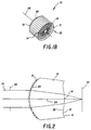
- the lenslet 10 is one element of a lenslet array that is formed with a number of lenslets.
- Each lenslet 10 is formed with a diffractive surface 18 formed on a refractive, spherical surface 20.
- Opposite the diffractive surface 18 is a second surface 22 that is an aspheric surface.
- the faceted surface of the diffractive surface 18 is seen more clearly in the cross-section of Fig. 2.
- the second surface is convex and transforms to a concave surface at the radius 12.
- the second surface 22 defines a polynomial asphere which exhibits an inflection at the radius 16. Both the first and the second surfaces are substantially perpendicular to the optical axis 24 of the lenslet 10.
- the lenslet 10 may be formed of optical glass such as BK7, quartz, injection molded plastic, or an epoxy replica.
- incident light rays 30 pass through an aperture stop array 40 and are focused onto a focal plane 50 by the lenslet 10.
- the diffractive/refractive surface comprised of 18 and 20 correct the chromatic aberrations and provide the majority of the focusing power while the aspheric surface 22 provides for correction of field dependent aberrations such as petzval curvature, astigmatism, and coma.
- the lens has an F# of 2.0 and a FL of 0.5mm, but generally could be from 0.4 to 2.0mm FL.
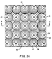
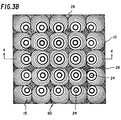
- the individual lenslets 10 of Figs. 1 and 2 are segmented and formed into a lenslet array 60.
- the lenslet array 60 is formed with the lenslets 10 being associated with corresponding photosensor sites 72 (shown more clearly in Fig. 4).
- the center of the optical axis 24 of each lenslet 10 is displaced outward as a function of its radial distance from the optical axis of the central lenslet while in Fig. 3B, the optical axes are displaced inward.
- the lines 15 appearing around the optical axis 24 of each lenslet 10 are topographical lines generally indicating changes in height of the lenslet's surface.
- An array of aperture stops 26 fills the areas between the lenslets 10 to prevent light from reaching the sensor that will be discussed with respect to Fig. 4.
- the array depicted in Figs. 3A and 3B represent only a small portion of an array that would be used in an actual camera. In an actual implementation approximately 260 X 214 to 1500 x 1000 lenslets are used to form the array 60. This invention does not form the lenslet array with the optical axis of each lenslet, and in turn the lenslet itself, aligned directly over a respective photosite in the CCD device.
- lenslets are displaced so as to form the image on a regularly spaced array of photosensors
- Other configurations of the lenslets may be used such as forming the outer periphery of each lenslet as a square, hexagon, or circle, without detracting from the invention.
- the reason that the invention uses only portions of the lenslets is that only a fraction of the lenslet is used for a particular angular field of view for an associated pixel of the group of three pixels for the color application.
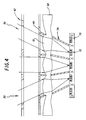
- Figure 4 is a cross-section taken along the section line 4-4 in Figs. 3A and 3B, illustrating the lenslet array 60 positioned over an image photosensor array 70 that may be a CCD array having a number of photosensitive sites 72 corresponding in number to at least the number of lenslets forming the array 60. In a three color environment up to three photosensitive sites would be formed under each corresponding lenslet.
- the lenslet array 60 is maintained a distance apart from the surfaces of the photosensors by spacers 74 that may also serve the function of being baffles.
- the aperture stop array 40 in combination with the baffles 74 and the field stop array 42 limit the field of view of any particular photosensor so that it does not overlap the field of view of it neighbors by a large amount.
- the field stop array 42 is positioned approximately 0.5mm to 2mm from the surface of the lenslet array 60.
- the center of the apertures in the aperture stop array and field stop array, 40 and 42, respectively are aligned to the center of the field of view of a corresponding lenslet.
- the spacing of the centers increases as a function of each lenslet's field angle from the center of the array causing the aperture stop array to be slightly larger than the associated lenslet array.
- the combination of the aperture stop array 40 with the field stop array 42 and a given lenslet focal length determines the field of view for a photosensitive site 72.
- the lenslet array 60 can be formed of etched quartz, or an epoxy replica on a glass substrate.
- the lenslets 10, combined with the appropriate field and aperture stop form images of a small segment of the field of view on photosensitive site 72.
- the light incident on a lenslet 10 is concentrated onto the active pixel area.
- any camera system incorporating the present invention can be extremely compact and flat.
- the camera can work in black and white or in color if three pixels with color filters are formed on each pixel are used.
- An array of aspheric lenslets can be used to form images on the detector array.
- the aforementioned embodiment does not correct for the variation in focal length as a function of wavelength since the lens element is formed from a single refractive material therefore the spot size of the incident light varies as a function of color.
- An improved optical design including a diffractive/refractive hybrid lens is used to correct the chromatic aberration in a single material.
- n( ⁇ ) [ ⁇ c / ⁇ ](n c -1)-1
- ⁇ c 587 nm
- ⁇ L 656 nm
- n diff and element power distribution can be calculated.
- the negative n diff of the diffractive surface allows for achromatization of single element hybrid refractive / diffractive lenses utilizing a positive focal length diffractive and refractive component. It also decreases the focal length and F/# required of the doublet component lenses because a refractive doublet consists of a positive crown (low dispersion) lens with a shorter focal length and smaller F/# than is required for a single element lens and a negative flint element which increases the doublet focal length to the correct value and compensates for the dispersion of the positive lens. This effect also decreases the size and weight of the positive element of a hybrid refractive / diffractive element.
- substrates such as quartz, or optical glass such as BK7, or utilize epoxy replicas on glass substrates.
- the use of diffractive/refractive hybrid achromatization enables the use of diffractive surfaces with longer focal lengths and higher F/#'s.
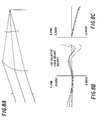
- the diffractive lenslets 10 are shown in Figs. 6A, 7A, and 8A, for the on-axis, 16 degrees, and full field of view. To be noted in a comparison of these figs is that the mechanical optical axis 14 is moving radially outwards as a function of field angle while the local optical axis 15 is incident normal to the plane of the photodetector array.
- the opaque mask 16 acts as the aperture stop for the system as well as limiting the field of view of a given photosensor
- Figs 6B, 6C, 7B, 7C, 8B, and 8C represent the tangential and saggital ray aberration curves for their respective lenslets. It is noteworthy that the overall spot size, including chromatic aberration, is approximately 10 microns which is a typical photodetector size.
- the solid lines represent a wavelength of 546.1 nm, the dotted lines represent a wavelength of 656.1 nm, and the dotted and dashed lines represent a wavelength of 460.0 nm which represent light in the green, red, and blue, wavelengths.
- the following table lists the optical design parameters for three array elements at 0, 16, and 26 degrees.
- the array elements at the intermediate field angles can be interpolated from these values.
Landscapes
- Physics & Mathematics (AREA)
- General Physics & Mathematics (AREA)
- Optics & Photonics (AREA)
- Color Television Image Signal Generators (AREA)
- Lenses (AREA)
- Optical Filters (AREA)
- Solid State Image Pick-Up Elements (AREA)
- Transforming Light Signals Into Electric Signals (AREA)
- Diffracting Gratings Or Hologram Optical Elements (AREA)
Applications Claiming Priority (2)
| Application Number | Priority Date | Filing Date | Title |
|---|---|---|---|
| US663887 | 1996-06-14 | ||
| US08/663,887 US5751492A (en) | 1996-06-14 | 1996-06-14 | Diffractive/Refractive lenslet array incorporating a second aspheric surface |
Publications (2)
| Publication Number | Publication Date |
|---|---|
| EP0813079A2 true EP0813079A2 (de) | 1997-12-17 |
| EP0813079A3 EP0813079A3 (de) | 1998-01-14 |
Family
ID=24663642
Family Applications (1)
| Application Number | Title | Priority Date | Filing Date |
|---|---|---|---|
| EP97108793A Withdrawn EP0813079A3 (de) | 1996-06-14 | 1997-06-02 | Eine diffraktive/refraktive Linsenmatrixanordnung mit einer zweiten asphärischen Fläche |
Country Status (3)
| Country | Link |
|---|---|
| US (1) | US5751492A (de) |
| EP (1) | EP0813079A3 (de) |
| JP (1) | JPH1084104A (de) |
Cited By (8)
| Publication number | Priority date | Publication date | Assignee | Title |
|---|---|---|---|---|
| WO2004057858A1 (en) * | 2002-12-20 | 2004-07-08 | Nokia Corporation | A color imaging system and a method in a color imaging system |
| GB2424123A (en) * | 2005-03-07 | 2006-09-13 | Agilent Technologies Inc | A bi-curvature lens for light emitting diodes and photodetectors |
| EP1865713A2 (de) | 2006-06-08 | 2007-12-12 | Funai Electric Co., Ltd. | Bildaufnahmesystem vom Typ eines Facettenauges |
| EP2018044A1 (de) * | 2007-07-18 | 2009-01-21 | Funai Electric Co., Ltd. | Abbildungssystem für ein Facettenauge |
| EP1665779B1 (de) * | 2004-01-20 | 2009-07-29 | Fraunhofer-Gesellschaft zur Förderung der angewandten Forschung e.V. | Bilderfassungssystem und dessen verwendung |
| CN103620782A (zh) * | 2011-07-08 | 2014-03-05 | 松下电器产业株式会社 | 固体摄像元件以及摄像装置 |
| DE102013226196A1 (de) * | 2013-12-17 | 2015-06-18 | Volkswagen Aktiengesellschaft | Optisches Sensorsystem |
| US10281745B2 (en) | 2014-05-28 | 2019-05-07 | Inoptec Limited Zweigniederlassung Deustchland | Electronic spectacles |
Families Citing this family (38)
| Publication number | Priority date | Publication date | Assignee | Title |
|---|---|---|---|---|
| JPH10329361A (ja) * | 1997-03-31 | 1998-12-15 | Ricoh Co Ltd | 光学装置、開口アレイの製造方法 |
| NO305728B1 (no) * | 1997-11-14 | 1999-07-12 | Reidar E Tangen | Optoelektronisk kamera og fremgangsmÕte ved bildeformatering i samme |
| US6552809B1 (en) * | 2000-09-18 | 2003-04-22 | Institut National D'optique | Position encoding optical device and method |
| JP2002171537A (ja) * | 2000-11-30 | 2002-06-14 | Canon Inc | 複眼撮像系、撮像装置および電子機器 |
| US20040012698A1 (en) * | 2001-03-05 | 2004-01-22 | Yasuo Suda | Image pickup model and image pickup device |
| US6635941B2 (en) | 2001-03-21 | 2003-10-21 | Canon Kabushiki Kaisha | Structure of semiconductor device with improved reliability |
| US6894719B2 (en) * | 2001-08-23 | 2005-05-17 | Eastman Kodak Company | Method and apparatus for creating a preselected lenticular image |
| JP2003143459A (ja) * | 2001-11-02 | 2003-05-16 | Canon Inc | 複眼撮像系およびこれを備えた装置 |
| US7423679B2 (en) * | 2002-12-20 | 2008-09-09 | Eastman Kodak Company | Imaging system having extended useful latitude |
| TWI289708B (en) | 2002-12-25 | 2007-11-11 | Qualcomm Mems Technologies Inc | Optical interference type color display |
| US7186969B2 (en) * | 2003-02-12 | 2007-03-06 | Mitutoyo Corporation | Optical configuration for imaging-type optical encoders |
| CN100476365C (zh) * | 2003-02-12 | 2009-04-08 | 三丰株式会社 | 位移检测光电式编码器 |
| US6801719B1 (en) * | 2003-03-14 | 2004-10-05 | Eastman Kodak Company | Camera using beam splitter with micro-lens image amplification |
| US7310477B2 (en) * | 2003-08-26 | 2007-12-18 | Eastman Kodak Company | Photographic film cartridge or cassette systems with microlens |
| US7511749B2 (en) * | 2003-12-18 | 2009-03-31 | Aptina Imaging Corporation | Color image sensor having imaging element array forming images on respective regions of sensor elements |
| EP1712087B1 (de) * | 2004-01-26 | 2021-03-10 | DigitalOptics Corporation | Dünne kamera mit subpixel-auflösung |
| US7342705B2 (en) | 2004-02-03 | 2008-03-11 | Idc, Llc | Spatial light modulator with integrated optical compensation structure |
| US7855824B2 (en) * | 2004-03-06 | 2010-12-21 | Qualcomm Mems Technologies, Inc. | Method and system for color optimization in a display |
| US8362987B2 (en) | 2004-09-27 | 2013-01-29 | Qualcomm Mems Technologies, Inc. | Method and device for manipulating color in a display |
| US7807488B2 (en) * | 2004-09-27 | 2010-10-05 | Qualcomm Mems Technologies, Inc. | Display element having filter material diffused in a substrate of the display element |
| US7710632B2 (en) * | 2004-09-27 | 2010-05-04 | Qualcomm Mems Technologies, Inc. | Display device having an array of spatial light modulators with integrated color filters |
| US7375312B2 (en) * | 2005-01-26 | 2008-05-20 | Avago Technologies Ecbu Ip Pte Ltd | Planar fly's eye detector |
| EP1764835B1 (de) * | 2005-09-19 | 2008-01-23 | CRF Societa'Consortile per Azioni | Multifunktioneller optischer Sensor mit einer an Mikrolinsen gekoppelten Matrix von Photodetektoren |
| WO2008045311A2 (en) | 2006-10-06 | 2008-04-17 | Qualcomm Mems Technologies, Inc. | Illumination device with built-in light coupler |
| EP1943551A2 (de) | 2006-10-06 | 2008-07-16 | Qualcomm Mems Technologies, Inc. | Lichtführung |
| EP2366945A1 (de) | 2006-10-06 | 2011-09-21 | Qualcomm Mems Technologies, Inc. | Beleuchtungseinrichtung einer Anzeigevorrichtung mit darin integrierter Struktur zur Erzeugung optischer Verluste |
| US8068710B2 (en) | 2007-12-07 | 2011-11-29 | Qualcomm Mems Technologies, Inc. | Decoupled holographic film and diffuser |
| US20100157406A1 (en) * | 2008-12-19 | 2010-06-24 | Qualcomm Mems Technologies, Inc. | System and method for matching light source emission to display element reflectivity |
| JP5359483B2 (ja) * | 2009-04-10 | 2013-12-04 | 住友電気工業株式会社 | 光合波器及びそれを用いた画像投影装置 |
| JP2010243987A (ja) * | 2009-04-10 | 2010-10-28 | Sumitomo Electric Ind Ltd | 光合波器及びそれを用いた画像投影装置 |
| CN102449511A (zh) | 2009-05-29 | 2012-05-09 | 高通Mems科技公司 | 照明装置及其制造方法 |
| US20110115916A1 (en) * | 2009-11-16 | 2011-05-19 | Eiji Yafuso | System for mosaic image acquisition |
| US8848294B2 (en) | 2010-05-20 | 2014-09-30 | Qualcomm Mems Technologies, Inc. | Method and structure capable of changing color saturation |
| US8670171B2 (en) | 2010-10-18 | 2014-03-11 | Qualcomm Mems Technologies, Inc. | Display having an embedded microlens array |
| US20120188391A1 (en) * | 2011-01-25 | 2012-07-26 | Scott Smith | Array camera having lenses with independent fields of view |
| WO2014197066A2 (en) * | 2013-03-14 | 2014-12-11 | Drs Rsta, Inc. | Single element radiometric lens |
| DE102015226476A1 (de) | 2014-12-25 | 2016-06-30 | Nichia Corporation | Lichtquellenvorrichtung |
| US11333748B2 (en) | 2018-09-17 | 2022-05-17 | Waymo Llc | Array of light detectors with corresponding array of optical elements |
Citations (5)
| Publication number | Priority date | Publication date | Assignee | Title |
|---|---|---|---|---|
| DE3146026A1 (de) * | 1980-11-20 | 1982-06-03 | Ricoh Co., Ltd., Tokyo | Abbildungseinrichtung |
| EP0560511A2 (de) * | 1992-03-09 | 1993-09-15 | AT&T Corp. | Optische Freiraumverbindungsanordnung |
| EP0608932A2 (de) * | 1993-01-25 | 1994-08-03 | Philips Electronics Uk Limited | Bildsensor |
| US5340978A (en) * | 1992-09-30 | 1994-08-23 | Lsi Logic Corporation | Image-sensing display panels with LCD display panel and photosensitive element array |
| US5497269A (en) * | 1992-06-25 | 1996-03-05 | Lockheed Missiles And Space Company, Inc. | Dispersive microlens |
Family Cites Families (36)
| Publication number | Priority date | Publication date | Assignee | Title |
|---|---|---|---|---|
| US3910683A (en) * | 1970-07-28 | 1975-10-07 | Minolta Camera Kk | Optical low-pass filter |
| JPS5010743B1 (de) * | 1970-12-26 | 1975-04-24 | ||
| US4093346A (en) * | 1973-07-13 | 1978-06-06 | Minolta Camera Kabushiki Kaisha | Optical low pass filter |
| JPS5742849B2 (de) * | 1974-06-05 | 1982-09-10 | ||
| JPS5813891B2 (ja) * | 1975-01-20 | 1983-03-16 | ミノルタ株式会社 | 光学的ロ−パスフィルタ− |
| US4318123A (en) * | 1980-06-05 | 1982-03-02 | Rca Corporation | Solid-state, color-encoding television camera |
| US4323925A (en) * | 1980-07-07 | 1982-04-06 | Avco Everett Research Laboratory, Inc. | Method and apparatus for arraying image sensor modules |
| US4377753A (en) * | 1981-06-01 | 1983-03-22 | Eastman Kodak Company | High resolution optical-addressing device and electronic scanner and/or printer apparatus employing such device |
| JPS61149923A (ja) * | 1984-12-25 | 1986-07-08 | Sony Corp | 位相型光学的ロ−パスフイルタ |
| US4708436A (en) * | 1985-07-12 | 1987-11-24 | Rca Corporation | Optical imager with diffractive lenticular array |
| US4689291A (en) * | 1985-08-30 | 1987-08-25 | Xerox Corporation | Pedestal-type microlens fabrication process |
| JPS62144459A (ja) * | 1985-12-19 | 1987-06-27 | Ricoh Co Ltd | 完全密着型センサ− |
| US5004901A (en) * | 1987-06-04 | 1991-04-02 | Mitsubishi Denki Kabushiki Kaisha | Current mirror amplifier for use in an optical data medium driving apparatus and servo-circuit |
| JP2600133B2 (ja) * | 1986-03-13 | 1997-04-16 | ブラザー工業株式会社 | 画像記録装置 |
| JP2605703B2 (ja) * | 1986-12-24 | 1997-04-30 | ソニー株式会社 | 撮像装置 |
| JPS63209288A (ja) * | 1987-02-25 | 1988-08-30 | Olympus Optical Co Ltd | 撮像装置 |
| JPH07111514B2 (ja) * | 1988-04-04 | 1995-11-29 | 日本放送協会 | 光学的ローパスフイルタ |
| US4989985A (en) * | 1988-09-19 | 1991-02-05 | Xerox Corporation | Densitometer for measuring specular reflectivity |
| JPH0833526B2 (ja) * | 1988-11-28 | 1996-03-29 | キヤノン株式会社 | 光学的ローパスフィルターを有した撮影レンズ |
| US5187358A (en) * | 1989-02-15 | 1993-02-16 | Canon Kabushiki Kaisha | Image reading device having a telecentric optical system and a blazed diffraction grating |
| US4994664A (en) * | 1989-03-27 | 1991-02-19 | Massachusetts Institute Of Technology | Optically coupled focal plane arrays using lenslets and multiplexers |
| US4989959A (en) * | 1989-06-12 | 1991-02-05 | Polaroid Corporation | Anti-aliasing optical system with pyramidal transparent structure |
| US5046827C1 (en) * | 1989-07-20 | 2001-08-07 | Honeywell Inc | Optical reconstruction filter for color mosaic displays |
| JP2800364B2 (ja) * | 1990-04-27 | 1998-09-21 | 松下電器産業株式会社 | 光学的ローパスフィルタ |
| US5151790A (en) * | 1990-07-23 | 1992-09-29 | Fuji Photo Film Co., Ltd. | Image pickup device for stabilizing optical aberrations |
| US5076687A (en) * | 1990-08-28 | 1991-12-31 | Massachusetts Institute Of Technology | Optical ranging apparatus |
| US5233431A (en) * | 1990-10-26 | 1993-08-03 | Fuji Photo Film Co., Ltd. | Image pickup device |
| US5309239A (en) * | 1991-07-11 | 1994-05-03 | U.S. Philips Corporation | Image pick-up device |
| US5233174A (en) * | 1992-03-11 | 1993-08-03 | Hughes Danbury Optical Systems, Inc. | Wavefront sensor having a lenslet array as a null corrector |
| US5294993A (en) * | 1992-04-10 | 1994-03-15 | Opton Corporation | Method and apparatus for using monochrome images to form a color image |
| JP2987016B2 (ja) * | 1992-08-28 | 1999-12-06 | 松下電器産業株式会社 | 位相格子光学的ローパスフィルタ |
| US5529936A (en) * | 1992-09-30 | 1996-06-25 | Lsi Logic Corporation | Method of etching a lens for a semiconductor solid state image sensor |
| US5349471A (en) * | 1993-02-16 | 1994-09-20 | The University Of Rochester | Hybrid refractive/diffractive achromatic lens for optical data storage systems |
| US5322998A (en) * | 1993-03-31 | 1994-06-21 | Eastman Kodak Company | Conical blur filter for reducing artifacts in imaging apparatus |
| US5471515A (en) * | 1994-01-28 | 1995-11-28 | California Institute Of Technology | Active pixel sensor with intra-pixel charge transfer |
| JPH08107194A (ja) * | 1994-10-03 | 1996-04-23 | Fuji Photo Optical Co Ltd | 固体撮像装置 |
-
1996
- 1996-06-14 US US08/663,887 patent/US5751492A/en not_active Expired - Lifetime
-
1997
- 1997-06-02 EP EP97108793A patent/EP0813079A3/de not_active Withdrawn
- 1997-06-16 JP JP15822397A patent/JPH1084104A/ja active Pending
Patent Citations (5)
| Publication number | Priority date | Publication date | Assignee | Title |
|---|---|---|---|---|
| DE3146026A1 (de) * | 1980-11-20 | 1982-06-03 | Ricoh Co., Ltd., Tokyo | Abbildungseinrichtung |
| EP0560511A2 (de) * | 1992-03-09 | 1993-09-15 | AT&T Corp. | Optische Freiraumverbindungsanordnung |
| US5497269A (en) * | 1992-06-25 | 1996-03-05 | Lockheed Missiles And Space Company, Inc. | Dispersive microlens |
| US5340978A (en) * | 1992-09-30 | 1994-08-23 | Lsi Logic Corporation | Image-sensing display panels with LCD display panel and photosensitive element array |
| EP0608932A2 (de) * | 1993-01-25 | 1994-08-03 | Philips Electronics Uk Limited | Bildsensor |
Non-Patent Citations (3)
| Title |
|---|
| JAHNS J ET AL: "PARALLEL OPTICAL INTERCONNECTIONS USING SURFACE-EMITTING MICROLASERS AND A HYBRID IMAGING SYSTEM" OPTICS COMMUNICATIONS, vol. 109, no. 3/04, 1 July 1994, pages 328-337, XP000448151 * |
| OGATA S ET AL: "OPTICAL SENSOR ARRAY IN AN ARTIFICIAL COMPOUND EYE" OPTICAL ENGINEERING, vol. 33, no. 11, 1 November 1994, pages 3649-3655, XP000475109 * |
| VELDKAMP W B ET AL: "BINARY OPTICS" SCIENTIFIC AMERICAN, vol. 266, no. 5, 1 May 1992, pages 50-55, XP000330991 * |
Cited By (13)
| Publication number | Priority date | Publication date | Assignee | Title |
|---|---|---|---|---|
| WO2004057858A1 (en) * | 2002-12-20 | 2004-07-08 | Nokia Corporation | A color imaging system and a method in a color imaging system |
| EP1665779B1 (de) * | 2004-01-20 | 2009-07-29 | Fraunhofer-Gesellschaft zur Förderung der angewandten Forschung e.V. | Bilderfassungssystem und dessen verwendung |
| GB2424123A (en) * | 2005-03-07 | 2006-09-13 | Agilent Technologies Inc | A bi-curvature lens for light emitting diodes and photodetectors |
| US7271963B2 (en) | 2005-03-07 | 2007-09-18 | Avago Technologies Ecbu Ip (Singapore) Pte. Ltd. | Bi-curvature lens for light emitting diodes and photo detectors |
| EP1865713A2 (de) | 2006-06-08 | 2007-12-12 | Funai Electric Co., Ltd. | Bildaufnahmesystem vom Typ eines Facettenauges |
| EP1865713A3 (de) * | 2006-06-08 | 2009-04-08 | Funai Electric Co., Ltd. | Bildaufnahmesystem vom Typ eines Facettenauges |
| EP2018044A1 (de) * | 2007-07-18 | 2009-01-21 | Funai Electric Co., Ltd. | Abbildungssystem für ein Facettenauge |
| CN103620782A (zh) * | 2011-07-08 | 2014-03-05 | 松下电器产业株式会社 | 固体摄像元件以及摄像装置 |
| CN103620782B (zh) * | 2011-07-08 | 2016-04-13 | 松下知识产权经营株式会社 | 固体摄像元件以及摄像装置 |
| DE102013226196A1 (de) * | 2013-12-17 | 2015-06-18 | Volkswagen Aktiengesellschaft | Optisches Sensorsystem |
| US10281745B2 (en) | 2014-05-28 | 2019-05-07 | Inoptec Limited Zweigniederlassung Deustchland | Electronic spectacles |
| EP4238621A2 (de) | 2014-05-28 | 2023-09-06 | Inoptec Limited | Elektronische brille |
| US11982882B2 (en) | 2014-05-28 | 2024-05-14 | Inoptec Limited Zweigniederlassung Deutschland | Electronic spectacles |
Also Published As
| Publication number | Publication date |
|---|---|
| JPH1084104A (ja) | 1998-03-31 |
| US5751492A (en) | 1998-05-12 |
| EP0813079A3 (de) | 1998-01-14 |
Similar Documents
| Publication | Publication Date | Title |
|---|---|---|
| EP0813079A2 (de) | Eine diffraktive/refraktive Linsenmatrixanordnung mit einer zweiten asphärischen Fläche | |
| US5696371A (en) | Diffractive/refractive lenslet array | |
| US5731899A (en) | Lenslet array system incorporating an integral field lens/reimager lenslet array | |
| US5822125A (en) | Lenslet array system | |
| US5796522A (en) | Lenslet array system with a baffle structure and a shutter | |
| US6940649B2 (en) | Wavefront coded imaging systems | |
| US5880879A (en) | Objective lens system utilizing diffractive optical element | |
| US8520325B2 (en) | Photographic lens optical system | |
| US8736985B2 (en) | Photographic lens optical system | |
| US8576489B2 (en) | Multihybrid artificial compound eye with varied ommatidia | |
| US5812322A (en) | Lenslet array system incorporating a field lenslet array | |
| US7042656B2 (en) | Compact wide-field-of-view imaging optical system | |
| CN107179598A (zh) | 光学成像系统 | |
| CN110161651A (zh) | 光学成像系统 | |
| EP0819952A2 (de) | Linse mit beugenden und asphärischen optischen Oberflächen | |
| US8432620B2 (en) | Photographic lens optical system | |
| JP2001083413A (ja) | 赤外線レンズ | |
| US20220137331A1 (en) | Imaging lens and imaging apparatus | |
| KR101079025B1 (ko) | 촬영 렌즈 광학계 | |
| KR102270189B1 (ko) | 렌즈 모듈의 성능을 평가하는 장치와 이에 적용될 수 있는 릴레이 렌즈계 | |
| CN109283666A (zh) | 光学成像系统 | |
| JPH10142497A (ja) | 赤外用光学系 | |
| JP3685278B2 (ja) | 撮像レンズ | |
| US6563654B2 (en) | External pupil lens system | |
| JP2001083412A (ja) | 赤外線レンズ |
Legal Events
| Date | Code | Title | Description |
|---|---|---|---|
| PUAI | Public reference made under article 153(3) epc to a published international application that has entered the european phase |
Free format text: ORIGINAL CODE: 0009012 |
|
| PUAL | Search report despatched |
Free format text: ORIGINAL CODE: 0009013 |
|
| AK | Designated contracting states |
Kind code of ref document: A2 Designated state(s): DE FR GB |
|
| AK | Designated contracting states |
Kind code of ref document: A3 Designated state(s): AT BE CH DE DK ES FI FR GB GR IE IT LI LU MC NL PT SE |
|
| 17P | Request for examination filed |
Effective date: 19980622 |
|
| AKX | Designation fees paid |
Free format text: DE FR GB |
|
| RBV | Designated contracting states (corrected) |
Designated state(s): DE FR GB |
|
| GRAG | Despatch of communication of intention to grant |
Free format text: ORIGINAL CODE: EPIDOS AGRA |
|
| 17Q | First examination report despatched |
Effective date: 20020625 |
|
| GRAG | Despatch of communication of intention to grant |
Free format text: ORIGINAL CODE: EPIDOS AGRA |
|
| GRAH | Despatch of communication of intention to grant a patent |
Free format text: ORIGINAL CODE: EPIDOS IGRA |
|
| STAA | Information on the status of an ep patent application or granted ep patent |
Free format text: STATUS: THE APPLICATION IS DEEMED TO BE WITHDRAWN |
|
| 18D | Application deemed to be withdrawn |
Effective date: 20030121 |