EP0813079A2 - A diffractive/refractive lenslet array incorporating a second aspheric surface - Google Patents
A diffractive/refractive lenslet array incorporating a second aspheric surface Download PDFInfo
- Publication number
- EP0813079A2 EP0813079A2 EP97108793A EP97108793A EP0813079A2 EP 0813079 A2 EP0813079 A2 EP 0813079A2 EP 97108793 A EP97108793 A EP 97108793A EP 97108793 A EP97108793 A EP 97108793A EP 0813079 A2 EP0813079 A2 EP 0813079A2
- Authority
- EP
- European Patent Office
- Prior art keywords
- array
- lenslet
- photosensors
- field
- focal length
- Prior art date
- Legal status (The legal status is an assumption and is not a legal conclusion. Google has not performed a legal analysis and makes no representation as to the accuracy of the status listed.)
- Withdrawn
Links
- 230000003287 optical effect Effects 0.000 claims abstract description 20
- 230000007704 transition Effects 0.000 claims 1
- 230000004075 alteration Effects 0.000 description 11
- 238000003491 array Methods 0.000 description 9
- 239000000758 substrate Substances 0.000 description 7
- 239000006185 dispersion Substances 0.000 description 5
- 238000013461 design Methods 0.000 description 4
- 239000000463 material Substances 0.000 description 4
- 238000012360 testing method Methods 0.000 description 4
- 239000004593 Epoxy Substances 0.000 description 3
- XUIMIQQOPSSXEZ-UHFFFAOYSA-N Silicon Chemical compound [Si] XUIMIQQOPSSXEZ-UHFFFAOYSA-N 0.000 description 3
- 239000012141 concentrate Substances 0.000 description 3
- 230000001419 dependent effect Effects 0.000 description 3
- 239000011521 glass Substances 0.000 description 3
- 238000004519 manufacturing process Methods 0.000 description 3
- 239000010453 quartz Substances 0.000 description 3
- 229910052710 silicon Inorganic materials 0.000 description 3
- 239000010703 silicon Substances 0.000 description 3
- VYPSYNLAJGMNEJ-UHFFFAOYSA-N silicon dioxide Inorganic materials O=[Si]=O VYPSYNLAJGMNEJ-UHFFFAOYSA-N 0.000 description 3
- 206010010071 Coma Diseases 0.000 description 2
- 239000003795 chemical substances by application Substances 0.000 description 2
- 238000012937 correction Methods 0.000 description 2
- 230000007423 decrease Effects 0.000 description 2
- 230000000694 effects Effects 0.000 description 2
- 238000003384 imaging method Methods 0.000 description 2
- 238000000034 method Methods 0.000 description 2
- 239000005304 optical glass Substances 0.000 description 2
- 239000004065 semiconductor Substances 0.000 description 2
- 125000006850 spacer group Chemical group 0.000 description 2
- 239000005294 BK7 Substances 0.000 description 1
- 238000004458 analytical method Methods 0.000 description 1
- 201000009310 astigmatism Diseases 0.000 description 1
- 238000005452 bending Methods 0.000 description 1
- 230000003247 decreasing effect Effects 0.000 description 1
- 238000002347 injection Methods 0.000 description 1
- 239000007924 injection Substances 0.000 description 1
- 238000012986 modification Methods 0.000 description 1
- 230000004048 modification Effects 0.000 description 1
- 239000002991 molded plastic Substances 0.000 description 1
- 239000004033 plastic Substances 0.000 description 1
- 229920003023 plastic Polymers 0.000 description 1
- 229920003229 poly(methyl methacrylate) Polymers 0.000 description 1
- 239000004926 polymethyl methacrylate Substances 0.000 description 1
- 238000012552 review Methods 0.000 description 1
- 238000000926 separation method Methods 0.000 description 1
- 238000001228 spectrum Methods 0.000 description 1
- 210000004243 sweat Anatomy 0.000 description 1
Images


Classifications
-
- G—PHYSICS
- G02—OPTICS
- G02B—OPTICAL ELEMENTS, SYSTEMS OR APPARATUS
- G02B5/00—Optical elements other than lenses
- G02B5/18—Diffraction gratings
- G02B5/1876—Diffractive Fresnel lenses; Zone plates; Kinoforms
-
- G—PHYSICS
- G02—OPTICS
- G02B—OPTICAL ELEMENTS, SYSTEMS OR APPARATUS
- G02B3/00—Simple or compound lenses
- G02B3/0006—Arrays
- G02B3/0037—Arrays characterized by the distribution or form of lenses
- G02B3/0043—Inhomogeneous or irregular arrays, e.g. varying shape, size, height
-
- G—PHYSICS
- G02—OPTICS
- G02B—OPTICAL ELEMENTS, SYSTEMS OR APPARATUS
- G02B3/00—Simple or compound lenses
- G02B3/0006—Arrays
- G02B3/0037—Arrays characterized by the distribution or form of lenses
- G02B3/0056—Arrays characterized by the distribution or form of lenses arranged along two different directions in a plane, e.g. honeycomb arrangement of lenses
-
- G—PHYSICS
- G02—OPTICS
- G02B—OPTICAL ELEMENTS, SYSTEMS OR APPARATUS
- G02B3/00—Simple or compound lenses
- G02B3/02—Simple or compound lenses with non-spherical faces
- G02B3/04—Simple or compound lenses with non-spherical faces with continuous faces that are rotationally symmetrical but deviate from a true sphere, e.g. so called "aspheric" lenses
-
- G—PHYSICS
- G02—OPTICS
- G02B—OPTICAL ELEMENTS, SYSTEMS OR APPARATUS
- G02B5/00—Optical elements other than lenses
- G02B5/18—Diffraction gratings
- G02B5/1876—Diffractive Fresnel lenses; Zone plates; Kinoforms
- G02B5/188—Plurality of such optical elements formed in or on a supporting substrate
- G02B5/1885—Arranged as a periodic array
-
- G—PHYSICS
- G02—OPTICS
- G02B—OPTICAL ELEMENTS, SYSTEMS OR APPARATUS
- G02B5/00—Optical elements other than lenses
- G02B5/18—Diffraction gratings
- G02B5/1876—Diffractive Fresnel lenses; Zone plates; Kinoforms
- G02B5/189—Structurally combined with optical elements not having diffractive power
- G02B5/1895—Structurally combined with optical elements not having diffractive power such optical elements having dioptric power
Definitions
- This invention is related to the field of lenslet arrays for image sensors and particularly to the field of lenslet arrays which when combined with digital image sensors form an electronic representation of the optical intensity distribution at the focal plane of the lenslet array.
- the minimum thickness of a camera is limited by the back focal distance of the camera objective. Focusing on digital cameras, it is possible to make digital cameras thinner by using wide angle lenses, but this makes objects appear as a smaller fraction of the field of view than is desired in some instances. There is also a limitation of the lens 1/2 field angle to be less than 30 to 35 degrees below which it is much easier to correct for field dependent aberrations such as coma, astigmation, lateral color, petzval field curvature and lateral color. This field angle limitation limits how short the focal length of the objective can be and in turn how thin a camera can be. It is the object of the current invention to form a very thin camera using a novel type of array lens photographic objective.
- Lenslets arrays have been used concentrate light imaged on the detector plane by a photographic objective into smaller areas to allow more of the incident light to fall on the photosensitive area of the photodetector array and less on insensitive area between the pixels. This has been described in papers such as "Visible Array Detectors" by Timothy J. Tredwell, from H O , V . 1, F , T , & D , S E , Chapter 22, pp. 32-34. These lenslet arrays are centered directly above the corresponding photosensor and are not designed to look at different portions of the field of view independently. Rather, they concentrate the light from an existing image formed by the photographic objective into the pixel aperture.
- the use of the widely separated pixels will greatly increase costs of the sensor since there will be fewer sensor arrays fabricated on a given size substrate or wafer. In addition, the larger sensor array size will cause a decreased yield of finished sensor arrays for a given manufacturing process. Also there is no discussion of the trade-off between the focal length of the lens array and the angular subtense of the pixels field of view. If the focal length of the lenslets is to short light from one part of the field of view which is incident on one pixel will also be within the field of view of an adjacent pixel. For very short focal lengths the corresponding pixel dimension required for an equivalent angular resolution will be so small as to not be able to be fabricated with lithographic processes.
- the light gathering area of the pixel will be so small as to not generate a reliably measurable number of electrons for a given incident intensity.
- diffractive/refractive hybrids for achromatization.
- the lenses will be abutted to each other and an opaque baffle placed over the sensor to limit the field of view of each pixel.
- a short focal length image sensor comprising:
- the lenslet 10 is one element of a lenslet array that is formed with a number of lenslets.
- Each lenslet 10 is formed with a diffractive surface 18 formed on a refractive, spherical surface 20.
- Opposite the diffractive surface 18 is a second surface 22 that is an aspheric surface.
- the faceted surface of the diffractive surface 18 is seen more clearly in the cross-section of Fig. 2.
- the second surface is convex and transforms to a concave surface at the radius 12.
- the second surface 22 defines a polynomial asphere which exhibits an inflection at the radius 16. Both the first and the second surfaces are substantially perpendicular to the optical axis 24 of the lenslet 10.
- the lenslet 10 may be formed of optical glass such as BK7, quartz, injection molded plastic, or an epoxy replica.
- incident light rays 30 pass through an aperture stop array 40 and are focused onto a focal plane 50 by the lenslet 10.
- the diffractive/refractive surface comprised of 18 and 20 correct the chromatic aberrations and provide the majority of the focusing power while the aspheric surface 22 provides for correction of field dependent aberrations such as petzval curvature, astigmatism, and coma.
- the lens has an F# of 2.0 and a FL of 0.5mm, but generally could be from 0.4 to 2.0mm FL.
- the individual lenslets 10 of Figs. 1 and 2 are segmented and formed into a lenslet array 60.
- the lenslet array 60 is formed with the lenslets 10 being associated with corresponding photosensor sites 72 (shown more clearly in Fig. 4).
- the center of the optical axis 24 of each lenslet 10 is displaced outward as a function of its radial distance from the optical axis of the central lenslet while in Fig. 3B, the optical axes are displaced inward.
- the lines 15 appearing around the optical axis 24 of each lenslet 10 are topographical lines generally indicating changes in height of the lenslet's surface.
- An array of aperture stops 26 fills the areas between the lenslets 10 to prevent light from reaching the sensor that will be discussed with respect to Fig. 4.
- the array depicted in Figs. 3A and 3B represent only a small portion of an array that would be used in an actual camera. In an actual implementation approximately 260 X 214 to 1500 x 1000 lenslets are used to form the array 60. This invention does not form the lenslet array with the optical axis of each lenslet, and in turn the lenslet itself, aligned directly over a respective photosite in the CCD device.
- lenslets are displaced so as to form the image on a regularly spaced array of photosensors
- Other configurations of the lenslets may be used such as forming the outer periphery of each lenslet as a square, hexagon, or circle, without detracting from the invention.
- the reason that the invention uses only portions of the lenslets is that only a fraction of the lenslet is used for a particular angular field of view for an associated pixel of the group of three pixels for the color application.
- Figure 4 is a cross-section taken along the section line 4-4 in Figs. 3A and 3B, illustrating the lenslet array 60 positioned over an image photosensor array 70 that may be a CCD array having a number of photosensitive sites 72 corresponding in number to at least the number of lenslets forming the array 60. In a three color environment up to three photosensitive sites would be formed under each corresponding lenslet.
- the lenslet array 60 is maintained a distance apart from the surfaces of the photosensors by spacers 74 that may also serve the function of being baffles.
- the aperture stop array 40 in combination with the baffles 74 and the field stop array 42 limit the field of view of any particular photosensor so that it does not overlap the field of view of it neighbors by a large amount.
- the field stop array 42 is positioned approximately 0.5mm to 2mm from the surface of the lenslet array 60.
- the center of the apertures in the aperture stop array and field stop array, 40 and 42, respectively are aligned to the center of the field of view of a corresponding lenslet.
- the spacing of the centers increases as a function of each lenslet's field angle from the center of the array causing the aperture stop array to be slightly larger than the associated lenslet array.
- the combination of the aperture stop array 40 with the field stop array 42 and a given lenslet focal length determines the field of view for a photosensitive site 72.
- the lenslet array 60 can be formed of etched quartz, or an epoxy replica on a glass substrate.
- the lenslets 10, combined with the appropriate field and aperture stop form images of a small segment of the field of view on photosensitive site 72.
- the light incident on a lenslet 10 is concentrated onto the active pixel area.
- any camera system incorporating the present invention can be extremely compact and flat.
- the camera can work in black and white or in color if three pixels with color filters are formed on each pixel are used.
- An array of aspheric lenslets can be used to form images on the detector array.
- the aforementioned embodiment does not correct for the variation in focal length as a function of wavelength since the lens element is formed from a single refractive material therefore the spot size of the incident light varies as a function of color.
- An improved optical design including a diffractive/refractive hybrid lens is used to correct the chromatic aberration in a single material.
- n( ⁇ ) [ ⁇ c / ⁇ ](n c -1)-1
- ⁇ c 587 nm
- ⁇ L 656 nm
- n diff and element power distribution can be calculated.
- the negative n diff of the diffractive surface allows for achromatization of single element hybrid refractive / diffractive lenses utilizing a positive focal length diffractive and refractive component. It also decreases the focal length and F/# required of the doublet component lenses because a refractive doublet consists of a positive crown (low dispersion) lens with a shorter focal length and smaller F/# than is required for a single element lens and a negative flint element which increases the doublet focal length to the correct value and compensates for the dispersion of the positive lens. This effect also decreases the size and weight of the positive element of a hybrid refractive / diffractive element.
- substrates such as quartz, or optical glass such as BK7, or utilize epoxy replicas on glass substrates.
- the use of diffractive/refractive hybrid achromatization enables the use of diffractive surfaces with longer focal lengths and higher F/#'s.
- the diffractive lenslets 10 are shown in Figs. 6A, 7A, and 8A, for the on-axis, 16 degrees, and full field of view. To be noted in a comparison of these figs is that the mechanical optical axis 14 is moving radially outwards as a function of field angle while the local optical axis 15 is incident normal to the plane of the photodetector array.
- the opaque mask 16 acts as the aperture stop for the system as well as limiting the field of view of a given photosensor
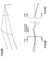
- Figs 6B, 6C, 7B, 7C, 8B, and 8C represent the tangential and saggital ray aberration curves for their respective lenslets. It is noteworthy that the overall spot size, including chromatic aberration, is approximately 10 microns which is a typical photodetector size.
- the solid lines represent a wavelength of 546.1 nm, the dotted lines represent a wavelength of 656.1 nm, and the dotted and dashed lines represent a wavelength of 460.0 nm which represent light in the green, red, and blue, wavelengths.
- the following table lists the optical design parameters for three array elements at 0, 16, and 26 degrees.
- the array elements at the intermediate field angles can be interpolated from these values.
Landscapes
- Physics & Mathematics (AREA)
- General Physics & Mathematics (AREA)
- Optics & Photonics (AREA)
- Color Television Image Signal Generators (AREA)
- Optical Filters (AREA)
- Solid State Image Pick-Up Elements (AREA)
- Transforming Light Signals Into Electric Signals (AREA)
- Diffracting Gratings Or Hologram Optical Elements (AREA)
- Lenses (AREA)
Abstract
- a color photosensor array comprised of sets of three photosensors with red, green, and blue, filters positioned over respective photosensors in each set;
- a lenslet array corresponding in the number of lenslets to the number of sets of photosensors in said color photosensor array, wherein each lenslet is formed with a first convex, spherical surface having diffractive means incorporated thereon and a second surface which is aspheric, substantially opposite said first surface with the size of said lenslet array being greater than the size of said photosensor array by an amount that allows the local optical axis of each lenslet at the largest field angle to image incident light onto the set of photosensors associated with the image sensors largest field angle; and
- an array of aperture stops combined with an array of field stops wherein the number of field and aperture stops corresponds to the number of lenslets and wherein each field and aperture stop is aligned to the center of the local optical axis for an associated set of photosensors.
Description
- This invention is related to the field of lenslet arrays for image sensors and particularly to the field of lenslet arrays which when combined with digital image sensors form an electronic representation of the optical intensity distribution at the focal plane of the lenslet array.
- The minimum thickness of a camera is limited by the back focal distance of the camera objective. Focusing on digital cameras, it is possible to make digital cameras thinner by using wide angle lenses, but this makes objects appear as a smaller fraction of the field of view than is desired in some instances. There is also a limitation of the lens 1/2 field angle to be less than 30 to 35 degrees below which it is much easier to correct for field dependent aberrations such as coma, astigmation, lateral color, petzval field curvature and lateral color. This field angle limitation limits how short the focal length of the objective can be and in turn how thin a camera can be. It is the object of the current invention to form a very thin camera using a novel type of array lens photographic objective.
- Lenslets arrays have been used concentrate light imaged on the detector plane by a photographic objective into smaller areas to allow more of the incident light to fall on the photosensitive area of the photodetector array and less on insensitive area between the pixels. This has been described in papers such as "Visible Array Detectors" by Timothy J. Tredwell, from H


 O
O


 , V
, V . 1, F


 , T
, T
 , & D
, & D , SE,
, SE,Chapter 22, pp. 32-34. These lenslet arrays are centered directly above the corresponding photosensor and are not designed to look at different portions of the field of view independently. Rather, they concentrate the light from an existing image formed by the photographic objective into the pixel aperture. - In U.S. Patent No. 4,994,664, entitled, "Optically Coupled Focal Plane Arrays Using Lenslets And Multiplexers" by Veldkamp, an array of diffractive lenslets is used to concentrate incident light onto an array of photosensors in order to allow for location of amplifying circuitry in areas between photosensor sites. These lenslets are centered over the photosensitive sites and are formed on the opposite side of the photosensor array on a silicon substrate, the use of the silicon substrate prevents them from imaging visible light onto the photosensors since silicon does not transmit in the visible wavelengths. This invention also would not be able to work over the visible wavelength range since the element is composed of all diffractive optical power and suffers from severe chromatic aberrations.
- In U.S. Patent No. 5,233,174, entitled, "Wavefront Sensor Having A Lenslet Array As A Null Corrector" by Zmek, an array of diffractive lenslets with decenters which are adjusted to eliminate the local monochromatic wavefront tilt from a specific optic under test in an interferometric or Hartman type test. A Hartman test is used to certify the surface quality of various optics. If the optics under test falls within the acceptance criteria the wavefront incident on the sensor array will form centered light spots on predetermined pixels. If the wavefront is other than the desired wavefront the light spots will be incident on different pixel elements. This invention is not applicable to the current application since the centered lenslets are not looking at regularly spaced sections of a predetermined field of view. It is also not applicable to white light applications due to the chromatic aberrations of the diffractive lenslets.
- U.S. Patent No. 5,340,978, entitled, "Image-Sensing Display With LCD Display Panel And Photosensitive Element Array" Rostoker et al., briefly describes an array of decentered lenses which form an image of a segment of the field of view is described. These lenses are widely separated and do not include a workable method for limiting a field of view seen by an individual pixel. Light from outside the desired field of view can be incident on the photosensor by scattering off the walls of a spacer element or by reflection and reimaging of light within the array substrate. The wide separation of the lenslets in the array limits the amount of light which can be gathered and focused on the image sensor. The use of the widely separated pixels will greatly increase costs of the sensor since there will be fewer sensor arrays fabricated on a given size substrate or wafer. In addition, the larger sensor array size will cause a decreased yield of finished sensor arrays for a given manufacturing process. Also there is no discussion of the trade-off between the focal length of the lens array and the angular subtense of the pixels field of view. If the focal length of the lenslets is to short light from one part of the field of view which is incident on one pixel will also be within the field of view of an adjacent pixel. For very short focal lengths the corresponding pixel dimension required for an equivalent angular resolution will be so small as to not be able to be fabricated with lithographic processes. In addition, the light gathering area of the pixel will be so small as to not generate a reliably measurable number of electrons for a given incident intensity. There is no discussion of the use of diffractive/refractive hybrids for achromatization. In the current invention the lenses will be abutted to each other and an opaque baffle placed over the sensor to limit the field of view of each pixel.
- The present invention is directed to overcoming one or more of the problems set forth above. Briefly summarized, according to one aspect of the present invention, there is provided a short focal length image sensor comprising:
- a color photosensor array comprised of sets of three photosensors with red, green, and blue, filters positioned over respective photosensors in each set;
- a lenslet array corresponding in the number of lenslets to the number of sets of photosensors in said color photosensor array, wherein each lenslet is formed with a first convex, spherical surface having diffractive means incorporated thereon and a second surface which is aspheric, substantially opposite said first surface with the size of said lenslet array being greater than the size of said photosensor array by an amount that allows the local optical axis of each lenslet at the largest field angle to image incident light onto the set of photosensors associated with the image sensors largest field angle; and
- an array of aperture stops combined with an array of field stops wherein the number of field and aperture stops corresponds to the number of lenslets and wherein each field and aperture stop is aligned to the center of the local optical axis for an associated set of photosensors.
- From the aforementioned it can be seen that it is a preferred object of the present invention to provide a lenslet array for an image sensor with a wide field of view and a short back focal distance.
- It is another object of the present invention to provide an improved lenslet array for use in a compact semiconductor image sensor assembly that is easy to fabricate and that enables the design and manufacture of cameras thinner than heretofore possible.
- These and other aspects, objects, features, and advantages of the present invention will be more clearly understood and appreciated from a review of the following detailed description of the preferred embodiments and appended claims, and by reference to the accompanying drawings.
- The present invention has the following advantages:
- The present lenslet array sensor is compact and portable due to its reduced lens backfocus which permits its use in very thin camera bodies;
- sensors incorporating the lenslet array of the present invention are easy to fabricate with minimum critical alignments of parts in that multiple integrated sensor arrays on a semiconductor wafer may be simultaneously aligned with multiple lenslet arrays before dicing of the wafer.
-
- Figs. 1A and 1B are a front and a rear perspective view of a lenslet formed in accord with the teachings of the present invention;
- Fig. 2 is a sectioned view taken along the section lines A-A of the lenslet of Fig 1B;
- Figs. 3A and 3B illustrates an aperture array positioned over a lenslet array with the spherical surface of each lenslet defined with topographical lines with the lenslets physical centers diverging with respect to photosensor centers in 3A and converging with respect to the photosensor centers in 3B;
- Fig. 4 illustrates, in a cross section view, an image sensor in accordance with the teachings of the present invention having an array of field stops and an array of aperture stops positioned in front of a lenslet array and photosensor array; and
- Fig. 5 illustrates, in a cross section view, an image sensor in accordance with the teachings of the present invention having an array of field stops positioned in front of a lenslet array and photosensor array and an array of aperture stops positioned between the lenslet array and the photosensor array;
- Figs. 6A, 6B, and 6C, illustrate a cross section of, the portion of a lenslet associated with a 0 degree field angle, the associated tangential, and saggital ray aberration curves, respectively;
- Figs. 7A, 7B, and 7C, illustrate a cross section of, the portion of a lenslet associated with a 14 degree field angle, the associated tangential, and saggital ray aberration curves, respectively; and
- Figs. 8A, 8B, and 8C, illustrate a cross section of, the portion of a lenslet associated with a 20 degree field angle, the associated tangential, and saggital ray aberration curves, respectively.
- To facilitate understanding, identical reference numerals have been used, where possible, to designate identical elements that are common to the figures.
- Referring to Figs. 1A and 1B, The
lenslet 10 is one element of a lenslet array that is formed with a number of lenslets. Eachlenslet 10 is formed with adiffractive surface 18 formed on a refractive,spherical surface 20. Opposite thediffractive surface 18 is asecond surface 22 that is an aspheric surface. The faceted surface of thediffractive surface 18 is seen more clearly in the cross-section of Fig. 2. At aradius 14 the second surface is convex and transforms to a concave surface at theradius 12. Thesecond surface 22 defines a polynomial asphere which exhibits an inflection at theradius 16. Both the first and the second surfaces are substantially perpendicular to theoptical axis 24 of thelenslet 10. Thelenslet 10 may be formed of optical glass such as BK7, quartz, injection molded plastic, or an epoxy replica. - Referring to Fig. 2, incident light rays 30 pass through an
aperture stop array 40 and are focused onto afocal plane 50 by thelenslet 10. The diffractive/refractive surface comprised of 18 and 20 correct the chromatic aberrations and provide the majority of the focusing power while theaspheric surface 22 provides for correction of field dependent aberrations such as petzval curvature, astigmatism, and coma. The lens has an F# of 2.0 and a FL of 0.5mm, but generally could be from 0.4 to 2.0mm FL. - Referring now to Figs. 3A and 3B, The
individual lenslets 10 of Figs. 1 and 2 are segmented and formed into alenslet array 60. Thelenslet array 60 is formed with thelenslets 10 being associated with corresponding photosensor sites 72 (shown more clearly in Fig. 4). To be observed in Figs. 3A and 3B is that the center of theoptical axis 24 of eachlenslet 10 is displaced outward as a function of its radial distance from the optical axis of the central lenslet while in Fig. 3B, the optical axes are displaced inward. Thelines 15 appearing around theoptical axis 24 of each lenslet 10 are topographical lines generally indicating changes in height of the lenslet's surface. An array of aperture stops 26 fills the areas between thelenslets 10 to prevent light from reaching the sensor that will be discussed with respect to Fig. 4. The array depicted in Figs. 3A and 3B represent only a small portion of an array that would be used in an actual camera. In an actual implementation approximately 260 X 214 to 1500 x 1000 lenslets are used to form thearray 60. This invention does not form the lenslet array with the optical axis of each lenslet, and in turn the lenslet itself, aligned directly over a respective photosite in the CCD device. Instead the lenslets are displaced so as to form the image on a regularly spaced array of photosensors Other configurations of the lenslets may be used such as forming the outer periphery of each lenslet as a square, hexagon, or circle, without detracting from the invention. - The reason that the invention uses only portions of the lenslets is that only a fraction of the lenslet is used for a particular angular field of view for an associated pixel of the group of three pixels for the color application.
- Figure 4 is a cross-section taken along the section line 4-4 in Figs. 3A and 3B, illustrating the
lenslet array 60 positioned over animage photosensor array 70 that may be a CCD array having a number ofphotosensitive sites 72 corresponding in number to at least the number of lenslets forming thearray 60. In a three color environment up to three photosensitive sites would be formed under each corresponding lenslet. Thelenslet array 60 is maintained a distance apart from the surfaces of the photosensors byspacers 74 that may also serve the function of being baffles. Theaperture stop array 40 in combination with thebaffles 74 and thefield stop array 42 limit the field of view of any particular photosensor so that it does not overlap the field of view of it neighbors by a large amount. Thefield stop array 42 is positioned approximately 0.5mm to 2mm from the surface of thelenslet array 60. - The center of the apertures in the aperture stop array and field stop array, 40 and 42, respectively are aligned to the center of the field of view of a corresponding lenslet. The spacing of the centers increases as a function of each lenslet's field angle from the center of the array causing the aperture stop array to be slightly larger than the associated lenslet array. The combination of the
aperture stop array 40 with thefield stop array 42 and a given lenslet focal length determines the field of view for aphotosensitive site 72. - The
lenslet array 60 can be formed of etched quartz, or an epoxy replica on a glass substrate. - The
lenslets 10, combined with the appropriate field and aperture stop form images of a small segment of the field of view onphotosensitive site 72. The light incident on alenslet 10 is concentrated onto the active pixel area. - The lenslet positions are adjusted to allow light imaged by the lenslet from a given field of view to be incident onto a given pixel. Since each CCD pixel has its own lens element there is no need to reinvert the image with a relay lens. Therefore, any camera system incorporating the present invention can be extremely compact and flat. The camera can work in black and white or in color if three pixels with color filters are formed on each pixel are used.
- An array of aspheric lenslets can be used to form images on the detector array. However, the aforementioned embodiment does not correct for the variation in focal length as a function of wavelength since the lens element is formed from a single refractive material therefore the spot size of the incident light varies as a function of color. An improved optical design including a diffractive/refractive hybrid lens is used to correct the chromatic aberration in a single material.
- The imaging properties of diffractive and holographic optics are strongly wavelength dependent. When modeling a diffractive optic this phenomena can be represented as a direct dependence of equivalent refractive index on wavelength:

- Diffractive elements impart all of their wavefront bending in an extremely thin layer. This is accounted for in the Sweat model by modeling the diffractive as a very high index material (nc = 10,000) with very low curvatures (weak surfaces) on each surface. The corresponding focal length can then be determined from:


The resultant dispersion νdiff of the diffractive element is:


- For other wavelength bands of interest an appropriate ndiff and element power distribution can be calculated. The direct dependence of the equivalent refractive index on wavelength leads to a small, negative, ndiff and a high level of wavelength dispersion associated with a first order (m = 1) diffractive optical element.
- Due to the variation of refractive index with wavelength a single element lens has a variation of focal length with wavelength. Two materials with different dispersions can be used to form a doublet lens which has the same focal length at two wavelengths and reduced variation over the whole spectrum. The relative distribution of focal powers required to achieve this is given by

- The negative ndiff of the diffractive surface allows for achromatization of single element hybrid refractive / diffractive lenses utilizing a positive focal length diffractive and refractive component. It also decreases the focal length and F/# required of the doublet component lenses because a refractive doublet consists of a positive crown (low dispersion) lens with a shorter focal length and smaller F/# than is required for a single element lens and a negative flint element which increases the doublet focal length to the correct value and compensates for the dispersion of the positive lens. This effect also decreases the size and weight of the positive element of a hybrid refractive / diffractive element.
- For traditional achromatization in the visible regime (d-e-f lines) with PMMA plastic lenses the fraction of power in the refractive and diffractive portions would be
- It is obvious to a person skilled in the art that one can utilize substrates such a quartz, or optical glass such as BK7, or utilize epoxy replicas on glass substrates.
- The use of diffractive/refractive hybrid achromatization enables the use of diffractive surfaces with longer focal lengths and higher F/#'s. The high F/# makes the diffractive element easier to manufacture due to the large zone spacings. For instance for a lens with a FL = 0.5 mm and a F/# = 2.0 the first order analysis of the refractive and diffractive portions would provide focal lengths and F/#'s of

- The
diffractive lenslets 10 are shown in Figs. 6A, 7A, and 8A, for the on-axis, 16 degrees, and full field of view. To be noted in a comparison of these figs is that the mechanicaloptical axis 14 is moving radially outwards as a function of field angle while the localoptical axis 15 is incident normal to the plane of the photodetector array. - The
opaque mask 16 acts as the aperture stop for the system as well as limiting the field of view of a given photosensor - Figs 6B, 6C, 7B, 7C, 8B, and 8C represent the tangential and saggital ray aberration curves for their respective lenslets. It is noteworthy that the overall spot size, including chromatic aberration, is approximately 10 microns which is a typical photodetector size. The solid lines represent a wavelength of 546.1 nm, the dotted lines represent a wavelength of 656.1 nm, and the dotted and dashed lines represent a wavelength of 460.0 nm which represent light in the green, red, and blue, wavelengths.
- The following table lists the optical design parameters for three array elements at 0, 16, and 26 degrees. The array elements at the intermediate field angles can be interpolated from these values.
-
- EFL = 0.5 mm
- F/# = 2.0
-
Surface No. Radius Thickness Glass Object Infinity Air 1 Aperture Stop 0.282 Air 2 0.38911 0.5 BK7 Diffractive Coefficients DF1 = -6.861 x 10⁻² DF2 = 6.568 x 10⁻¹ DF3 = 3.453 x 10⁻³ DF4 = -1.435 x 10² DF5 = 1.398 x 10³ 3 -0.50499 0.25715 Air Aspheric Coefficients AD = 0.18542 x 10² AE = -0.44635 x 10³ AF = 0.10191 x 10⁵ AG = -0.70929 x 10⁵ AH = 0.78203 X 10⁵ Image Air 


- The invention has been described with reference to a preferred embodiment. However, it will be appreciated that variations and modifications can be effected by a person of ordinary skill in the art without departing from the scope of the invention.
-
- 10
- lenslet
- 12
- radius
- 14
- radius
- 15
- lines
- 16
- radius
- 18
- diffractive surface
- 20
- refractive, spherical surface
- 22
- second surface
- 24
- optical axis
- 26
- aperture steps
- 30
- incident light rays
- 40
- aperture stop array
- 42
- field stop array
- 50
- focal plane
- 60
- lenslet array
- 70
- image photosensor array
- 72
- photosensitive sites
- 74
- baffles
Claims (7)
- A short focal length image sensor comprising:a color photosensor array comprised of sets of three photosensors with red, green, and blue, filters positioned over respective photosensors in each set;a lenslet array corresponding in the number of lenslets to the number of sets of photosensors in said color photosensor array, wherein each lenslet is formed with a first convex, spherical surface having diffractive means incorporated thereon and a second surface which is aspheric, substantially opposite said first surface with the size of said lenslet array being greater than the size of said photosensor array by an amount that allows the local optical axis of each lenslet at the largest field angle to image incident light onto the set of photosensors associated with the image sensors largest field angle; andan array of aperture stops combined with an array of field stops wherein the number of field and aperture stops corresponds to the number of lenslets and wherein each field and aperture stop is aligned to the center of the local optical axis for an associated set of photosensors.
- The short focal length image sensor according to Claim 1 wherein the second surface of each lenslet is an aspheric surface that is convex at the lenses physical center and transitions to a concave surface towards the edge of the lens.
- The short focal length image sensor according to Claim 1 wherein said array of aperture stops is positioned in front of said lenslet array.
- The short focal length image sensor according to Claim 1 wherein said array of aperture stops is positioned between said lenslet array and said array of photosensors.
- The short focal length image sensor according to Claim 1 wherein the lenslets of said array of lenslets are abutting.
- The short focal length image sensor according to Claim 1 wherein each lenslet is positioned in said array so as to view a different fraction of the total field of view of the image sensor.
- The short focal length image sensor according to Claim 1 and further comprising a plurality of baffles extending between each lenslet and an associated set of photosensors for preventing stray light from an adjacent lenslet impinging on the associated set of photosensors.
Applications Claiming Priority (2)
| Application Number | Priority Date | Filing Date | Title |
|---|---|---|---|
| US663887 | 1996-06-14 | ||
| US08/663,887 US5751492A (en) | 1996-06-14 | 1996-06-14 | Diffractive/Refractive lenslet array incorporating a second aspheric surface |
Publications (2)
| Publication Number | Publication Date |
|---|---|
| EP0813079A2 true EP0813079A2 (en) | 1997-12-17 |
| EP0813079A3 EP0813079A3 (en) | 1998-01-14 |
Family
ID=24663642
Family Applications (1)
| Application Number | Title | Priority Date | Filing Date |
|---|---|---|---|
| EP97108793A Withdrawn EP0813079A3 (en) | 1996-06-14 | 1997-06-02 | A diffractive/refractive lenslet array incorporating a second aspheric surface |
Country Status (3)
| Country | Link |
|---|---|
| US (1) | US5751492A (en) |
| EP (1) | EP0813079A3 (en) |
| JP (1) | JPH1084104A (en) |
Cited By (8)
| Publication number | Priority date | Publication date | Assignee | Title |
|---|---|---|---|---|
| WO2004057858A1 (en) * | 2002-12-20 | 2004-07-08 | Nokia Corporation | A color imaging system and a method in a color imaging system |
| GB2424123A (en) * | 2005-03-07 | 2006-09-13 | Agilent Technologies Inc | A bi-curvature lens for light emitting diodes and photodetectors |
| EP1865713A2 (en) | 2006-06-08 | 2007-12-12 | Funai Electric Co., Ltd. | Compound-eye imaging device |
| EP2018044A1 (en) * | 2007-07-18 | 2009-01-21 | Funai Electric Co., Ltd. | Compound-eye imaging device |
| EP1665779B1 (en) * | 2004-01-20 | 2009-07-29 | Fraunhofer-Gesellschaft zur Förderung der angewandten Forschung e.V. | Image recording system, and use thereof |
| CN103620782A (en) * | 2011-07-08 | 2014-03-05 | 松下电器产业株式会社 | Solid-state imaging element and imaging device |
| DE102013226196A1 (en) * | 2013-12-17 | 2015-06-18 | Volkswagen Aktiengesellschaft | Optical sensor system |
| US10281745B2 (en) | 2014-05-28 | 2019-05-07 | Inoptec Limited Zweigniederlassung Deustchland | Electronic spectacles |
Families Citing this family (40)
| Publication number | Priority date | Publication date | Assignee | Title |
|---|---|---|---|---|
| JPH10329361A (en) * | 1997-03-31 | 1998-12-15 | Ricoh Co Ltd | Manufacture of optical apparatus and opening array |
| NO305728B1 (en) * | 1997-11-14 | 1999-07-12 | Reidar E Tangen | Optoelectronic camera and method of image formatting in the same |
| US6552809B1 (en) * | 2000-09-18 | 2003-04-22 | Institut National D'optique | Position encoding optical device and method |
| JP2002171537A (en) * | 2000-11-30 | 2002-06-14 | Canon Inc | Compound image pickup system, image pickup device and electronic device |
| US20040012698A1 (en) * | 2001-03-05 | 2004-01-22 | Yasuo Suda | Image pickup model and image pickup device |
| US6635941B2 (en) | 2001-03-21 | 2003-10-21 | Canon Kabushiki Kaisha | Structure of semiconductor device with improved reliability |
| US6894719B2 (en) * | 2001-08-23 | 2005-05-17 | Eastman Kodak Company | Method and apparatus for creating a preselected lenticular image |
| JP2003143459A (en) * | 2001-11-02 | 2003-05-16 | Canon Inc | Compound-eye image pickup system and device provided therewith |
| US7423679B2 (en) * | 2002-12-20 | 2008-09-09 | Eastman Kodak Company | Imaging system having extended useful latitude |
| TWI289708B (en) | 2002-12-25 | 2007-11-11 | Qualcomm Mems Technologies Inc | Optical interference type color display |
| CN100476365C (en) * | 2003-02-12 | 2009-04-08 | 三丰株式会社 | Photoelectric encoder for detecting displacement |
| US7186969B2 (en) * | 2003-02-12 | 2007-03-06 | Mitutoyo Corporation | Optical configuration for imaging-type optical encoders |
| US6801719B1 (en) * | 2003-03-14 | 2004-10-05 | Eastman Kodak Company | Camera using beam splitter with micro-lens image amplification |
| US7310477B2 (en) * | 2003-08-26 | 2007-12-18 | Eastman Kodak Company | Photographic film cartridge or cassette systems with microlens |
| US7511749B2 (en) * | 2003-12-18 | 2009-03-31 | Aptina Imaging Corporation | Color image sensor having imaging element array forming images on respective regions of sensor elements |
| WO2005072370A2 (en) * | 2004-01-26 | 2005-08-11 | Digital Optics Corporation | Thin camera having sub-pixel resolution |
| US7342705B2 (en) | 2004-02-03 | 2008-03-11 | Idc, Llc | Spatial light modulator with integrated optical compensation structure |
| US7855824B2 (en) * | 2004-03-06 | 2010-12-21 | Qualcomm Mems Technologies, Inc. | Method and system for color optimization in a display |
| US8362987B2 (en) | 2004-09-27 | 2013-01-29 | Qualcomm Mems Technologies, Inc. | Method and device for manipulating color in a display |
| US7807488B2 (en) * | 2004-09-27 | 2010-10-05 | Qualcomm Mems Technologies, Inc. | Display element having filter material diffused in a substrate of the display element |
| US7710632B2 (en) * | 2004-09-27 | 2010-05-04 | Qualcomm Mems Technologies, Inc. | Display device having an array of spatial light modulators with integrated color filters |
| US7375312B2 (en) * | 2005-01-26 | 2008-05-20 | Avago Technologies Ecbu Ip Pte Ltd | Planar fly's eye detector |
| ATE385044T1 (en) * | 2005-09-19 | 2008-02-15 | Fiat Ricerche | MULTIFUNCTIONAL OPTICAL SENSOR WITH A MATRIX OF PHOTODETECTORS COUPLED TO MICRO LENSES |
| EP1943555B1 (en) | 2006-10-06 | 2012-05-02 | QUALCOMM MEMS Technologies, Inc. | Optical loss structure integrated in an illumination apparatus of a display |
| WO2008045207A2 (en) | 2006-10-06 | 2008-04-17 | Qualcomm Mems Technologies, Inc. | Light guide |
| WO2008045311A2 (en) | 2006-10-06 | 2008-04-17 | Qualcomm Mems Technologies, Inc. | Illumination device with built-in light coupler |
| US8068710B2 (en) | 2007-12-07 | 2011-11-29 | Qualcomm Mems Technologies, Inc. | Decoupled holographic film and diffuser |
| US20100157406A1 (en) * | 2008-12-19 | 2010-06-24 | Qualcomm Mems Technologies, Inc. | System and method for matching light source emission to display element reflectivity |
| JP2010243987A (en) * | 2009-04-10 | 2010-10-28 | Sumitomo Electric Ind Ltd | Optical combiner and image projector using the optical combiner |
| JP5359483B2 (en) * | 2009-04-10 | 2013-12-04 | 住友電気工業株式会社 | Optical multiplexer and image projection apparatus using the same |
| US9121979B2 (en) | 2009-05-29 | 2015-09-01 | Qualcomm Mems Technologies, Inc. | Illumination devices and methods of fabrication thereof |
| US20110115916A1 (en) * | 2009-11-16 | 2011-05-19 | Eiji Yafuso | System for mosaic image acquisition |
| US8848294B2 (en) | 2010-05-20 | 2014-09-30 | Qualcomm Mems Technologies, Inc. | Method and structure capable of changing color saturation |
| US8670171B2 (en) | 2010-10-18 | 2014-03-11 | Qualcomm Mems Technologies, Inc. | Display having an embedded microlens array |
| US20120188391A1 (en) * | 2011-01-25 | 2012-07-26 | Scott Smith | Array camera having lenses with independent fields of view |
| WO2014197066A2 (en) * | 2013-03-14 | 2014-12-11 | Drs Rsta, Inc. | Single element radiometric lens |
| DE102015226476A1 (en) | 2014-12-25 | 2016-06-30 | Nichia Corporation | Light source device |
| US11333748B2 (en) | 2018-09-17 | 2022-05-17 | Waymo Llc | Array of light detectors with corresponding array of optical elements |
| GB201916641D0 (en) | 2019-11-15 | 2020-01-01 | Renishaw Plc | Position measurement device |
| GB201916662D0 (en) | 2019-11-15 | 2020-01-01 | Renishaw Plc | Encoder apparatus |
Citations (5)
| Publication number | Priority date | Publication date | Assignee | Title |
|---|---|---|---|---|
| DE3146026A1 (en) * | 1980-11-20 | 1982-06-03 | Ricoh Co., Ltd., Tokyo | Imaging device |
| EP0560511A2 (en) * | 1992-03-09 | 1993-09-15 | AT&T Corp. | Free-space optical interconnection arrangement |
| EP0608932A2 (en) * | 1993-01-25 | 1994-08-03 | Philips Electronics Uk Limited | An image sensor |
| US5340978A (en) * | 1992-09-30 | 1994-08-23 | Lsi Logic Corporation | Image-sensing display panels with LCD display panel and photosensitive element array |
| US5497269A (en) * | 1992-06-25 | 1996-03-05 | Lockheed Missiles And Space Company, Inc. | Dispersive microlens |
Family Cites Families (36)
| Publication number | Priority date | Publication date | Assignee | Title |
|---|---|---|---|---|
| US3910683A (en) * | 1970-07-28 | 1975-10-07 | Minolta Camera Kk | Optical low-pass filter |
| JPS5010743B1 (en) * | 1970-12-26 | 1975-04-24 | ||
| US4093346A (en) * | 1973-07-13 | 1978-06-06 | Minolta Camera Kabushiki Kaisha | Optical low pass filter |
| JPS5742849B2 (en) * | 1974-06-05 | 1982-09-10 | ||
| JPS5813891B2 (en) * | 1975-01-20 | 1983-03-16 | ミノルタ株式会社 | optical low pass filter |
| US4318123A (en) * | 1980-06-05 | 1982-03-02 | Rca Corporation | Solid-state, color-encoding television camera |
| US4323925A (en) * | 1980-07-07 | 1982-04-06 | Avco Everett Research Laboratory, Inc. | Method and apparatus for arraying image sensor modules |
| US4377753A (en) * | 1981-06-01 | 1983-03-22 | Eastman Kodak Company | High resolution optical-addressing device and electronic scanner and/or printer apparatus employing such device |
| JPS61149923A (en) * | 1984-12-25 | 1986-07-08 | Sony Corp | Optical low-pass filter of phase type |
| US4708436A (en) * | 1985-07-12 | 1987-11-24 | Rca Corporation | Optical imager with diffractive lenticular array |
| US4689291A (en) * | 1985-08-30 | 1987-08-25 | Xerox Corporation | Pedestal-type microlens fabrication process |
| JPS62144459A (en) * | 1985-12-19 | 1987-06-27 | Ricoh Co Ltd | Complete contact type sensor |
| US5004901A (en) * | 1987-06-04 | 1991-04-02 | Mitsubishi Denki Kabushiki Kaisha | Current mirror amplifier for use in an optical data medium driving apparatus and servo-circuit |
| JP2600133B2 (en) * | 1986-03-13 | 1997-04-16 | ブラザー工業株式会社 | Image recording device |
| JP2605703B2 (en) * | 1986-12-24 | 1997-04-30 | ソニー株式会社 | Imaging device |
| JPS63209288A (en) * | 1987-02-25 | 1988-08-30 | Olympus Optical Co Ltd | Image pickup device |
| JPH07111514B2 (en) * | 1988-04-04 | 1995-11-29 | 日本放送協会 | Optical low pass filter |
| US4989985A (en) * | 1988-09-19 | 1991-02-05 | Xerox Corporation | Densitometer for measuring specular reflectivity |
| JPH0833526B2 (en) * | 1988-11-28 | 1996-03-29 | キヤノン株式会社 | Photographic lens with optical low-pass filter |
| US5187358A (en) * | 1989-02-15 | 1993-02-16 | Canon Kabushiki Kaisha | Image reading device having a telecentric optical system and a blazed diffraction grating |
| US4994664A (en) * | 1989-03-27 | 1991-02-19 | Massachusetts Institute Of Technology | Optically coupled focal plane arrays using lenslets and multiplexers |
| US4989959A (en) * | 1989-06-12 | 1991-02-05 | Polaroid Corporation | Anti-aliasing optical system with pyramidal transparent structure |
| US5046827C1 (en) * | 1989-07-20 | 2001-08-07 | Honeywell Inc | Optical reconstruction filter for color mosaic displays |
| JP2800364B2 (en) * | 1990-04-27 | 1998-09-21 | 松下電器産業株式会社 | Optical low-pass filter |
| US5151790A (en) * | 1990-07-23 | 1992-09-29 | Fuji Photo Film Co., Ltd. | Image pickup device for stabilizing optical aberrations |
| US5076687A (en) * | 1990-08-28 | 1991-12-31 | Massachusetts Institute Of Technology | Optical ranging apparatus |
| US5233431A (en) * | 1990-10-26 | 1993-08-03 | Fuji Photo Film Co., Ltd. | Image pickup device |
| US5309239A (en) * | 1991-07-11 | 1994-05-03 | U.S. Philips Corporation | Image pick-up device |
| US5233174A (en) * | 1992-03-11 | 1993-08-03 | Hughes Danbury Optical Systems, Inc. | Wavefront sensor having a lenslet array as a null corrector |
| US5294993A (en) * | 1992-04-10 | 1994-03-15 | Opton Corporation | Method and apparatus for using monochrome images to form a color image |
| JP2987016B2 (en) * | 1992-08-28 | 1999-12-06 | 松下電器産業株式会社 | Phase grating optical low-pass filter |
| US5529936A (en) * | 1992-09-30 | 1996-06-25 | Lsi Logic Corporation | Method of etching a lens for a semiconductor solid state image sensor |
| US5349471A (en) * | 1993-02-16 | 1994-09-20 | The University Of Rochester | Hybrid refractive/diffractive achromatic lens for optical data storage systems |
| US5322998A (en) * | 1993-03-31 | 1994-06-21 | Eastman Kodak Company | Conical blur filter for reducing artifacts in imaging apparatus |
| US5471515A (en) * | 1994-01-28 | 1995-11-28 | California Institute Of Technology | Active pixel sensor with intra-pixel charge transfer |
| JPH08107194A (en) * | 1994-10-03 | 1996-04-23 | Fuji Photo Optical Co Ltd | Solid state image sensor |
-
1996
- 1996-06-14 US US08/663,887 patent/US5751492A/en not_active Expired - Lifetime
-
1997
- 1997-06-02 EP EP97108793A patent/EP0813079A3/en not_active Withdrawn
- 1997-06-16 JP JP15822397A patent/JPH1084104A/en active Pending
Patent Citations (5)
| Publication number | Priority date | Publication date | Assignee | Title |
|---|---|---|---|---|
| DE3146026A1 (en) * | 1980-11-20 | 1982-06-03 | Ricoh Co., Ltd., Tokyo | Imaging device |
| EP0560511A2 (en) * | 1992-03-09 | 1993-09-15 | AT&T Corp. | Free-space optical interconnection arrangement |
| US5497269A (en) * | 1992-06-25 | 1996-03-05 | Lockheed Missiles And Space Company, Inc. | Dispersive microlens |
| US5340978A (en) * | 1992-09-30 | 1994-08-23 | Lsi Logic Corporation | Image-sensing display panels with LCD display panel and photosensitive element array |
| EP0608932A2 (en) * | 1993-01-25 | 1994-08-03 | Philips Electronics Uk Limited | An image sensor |
Non-Patent Citations (3)
| Title |
|---|
| JAHNS J ET AL: "PARALLEL OPTICAL INTERCONNECTIONS USING SURFACE-EMITTING MICROLASERS AND A HYBRID IMAGING SYSTEM" OPTICS COMMUNICATIONS, vol. 109, no. 3/04, 1 July 1994, pages 328-337, XP000448151 * |
| OGATA S ET AL: "OPTICAL SENSOR ARRAY IN AN ARTIFICIAL COMPOUND EYE" OPTICAL ENGINEERING, vol. 33, no. 11, 1 November 1994, pages 3649-3655, XP000475109 * |
| VELDKAMP W B ET AL: "BINARY OPTICS" SCIENTIFIC AMERICAN, vol. 266, no. 5, 1 May 1992, pages 50-55, XP000330991 * |
Cited By (13)
| Publication number | Priority date | Publication date | Assignee | Title |
|---|---|---|---|---|
| WO2004057858A1 (en) * | 2002-12-20 | 2004-07-08 | Nokia Corporation | A color imaging system and a method in a color imaging system |
| EP1665779B1 (en) * | 2004-01-20 | 2009-07-29 | Fraunhofer-Gesellschaft zur Förderung der angewandten Forschung e.V. | Image recording system, and use thereof |
| GB2424123A (en) * | 2005-03-07 | 2006-09-13 | Agilent Technologies Inc | A bi-curvature lens for light emitting diodes and photodetectors |
| US7271963B2 (en) | 2005-03-07 | 2007-09-18 | Avago Technologies Ecbu Ip (Singapore) Pte. Ltd. | Bi-curvature lens for light emitting diodes and photo detectors |
| EP1865713A2 (en) | 2006-06-08 | 2007-12-12 | Funai Electric Co., Ltd. | Compound-eye imaging device |
| EP1865713A3 (en) * | 2006-06-08 | 2009-04-08 | Funai Electric Co., Ltd. | Compound-eye imaging device |
| EP2018044A1 (en) * | 2007-07-18 | 2009-01-21 | Funai Electric Co., Ltd. | Compound-eye imaging device |
| CN103620782A (en) * | 2011-07-08 | 2014-03-05 | 松下电器产业株式会社 | Solid-state imaging element and imaging device |
| CN103620782B (en) * | 2011-07-08 | 2016-04-13 | 松下知识产权经营株式会社 | Solid-state imager and camera head |
| DE102013226196A1 (en) * | 2013-12-17 | 2015-06-18 | Volkswagen Aktiengesellschaft | Optical sensor system |
| US10281745B2 (en) | 2014-05-28 | 2019-05-07 | Inoptec Limited Zweigniederlassung Deustchland | Electronic spectacles |
| EP4238621A2 (en) | 2014-05-28 | 2023-09-06 | Inoptec Limited | Electronic eyewear |
| US11982882B2 (en) | 2014-05-28 | 2024-05-14 | Inoptec Limited Zweigniederlassung Deutschland | Electronic spectacles |
Also Published As
| Publication number | Publication date |
|---|---|
| EP0813079A3 (en) | 1998-01-14 |
| JPH1084104A (en) | 1998-03-31 |
| US5751492A (en) | 1998-05-12 |
Similar Documents
| Publication | Publication Date | Title |
|---|---|---|
| EP0813079A2 (en) | A diffractive/refractive lenslet array incorporating a second aspheric surface | |
| US5696371A (en) | Diffractive/refractive lenslet array | |
| US5731899A (en) | Lenslet array system incorporating an integral field lens/reimager lenslet array | |
| US5822125A (en) | Lenslet array system | |
| CN118295106A (en) | Optical imaging lens | |
| US6940649B2 (en) | Wavefront coded imaging systems | |
| US5880879A (en) | Objective lens system utilizing diffractive optical element | |
| US8520325B2 (en) | Photographic lens optical system | |
| US8736985B2 (en) | Photographic lens optical system | |
| US8576489B2 (en) | Multihybrid artificial compound eye with varied ommatidia | |
| CN107203027A (en) | Optical imaging system | |
| US5812322A (en) | Lenslet array system incorporating a field lenslet array | |
| CN110161651A (en) | Optical imaging system | |
| US7042656B2 (en) | Compact wide-field-of-view imaging optical system | |
| CN107179598A (en) | Optical imaging system | |
| JP2001083413A (en) | Infrared lens | |
| EP0819952A2 (en) | Lens with diffractive and aspheric surfaces | |
| US8432620B2 (en) | Photographic lens optical system | |
| CN109283666A (en) | Optical imaging system | |
| KR101079025B1 (en) | Photographic lens optical system | |
| KR102270189B1 (en) | Apparatus for evaluating performance of lens module and relay lens system applicable thereto | |
| JP7225047B2 (en) | Imaging lens and imaging device | |
| JPH10142497A (en) | Infrared optical system | |
| JP3685278B2 (en) | Imaging lens | |
| US20020149856A1 (en) | External pupil lens system |
Legal Events
| Date | Code | Title | Description |
|---|---|---|---|
| PUAI | Public reference made under article 153(3) epc to a published international application that has entered the european phase |
Free format text: ORIGINAL CODE: 0009012 |
|
| PUAL | Search report despatched |
Free format text: ORIGINAL CODE: 0009013 |
|
| AK | Designated contracting states |
Kind code of ref document: A2 Designated state(s): DE FR GB |
|
| AK | Designated contracting states |
Kind code of ref document: A3 Designated state(s): AT BE CH DE DK ES FI FR GB GR IE IT LI LU MC NL PT SE |
|
| 17P | Request for examination filed |
Effective date: 19980622 |
|
| AKX | Designation fees paid |
Free format text: DE FR GB |
|
| RBV | Designated contracting states (corrected) |
Designated state(s): DE FR GB |
|
| GRAG | Despatch of communication of intention to grant |
Free format text: ORIGINAL CODE: EPIDOS AGRA |
|
| 17Q | First examination report despatched |
Effective date: 20020625 |
|
| GRAG | Despatch of communication of intention to grant |
Free format text: ORIGINAL CODE: EPIDOS AGRA |
|
| GRAH | Despatch of communication of intention to grant a patent |
Free format text: ORIGINAL CODE: EPIDOS IGRA |
|
| STAA | Information on the status of an ep patent application or granted ep patent |
Free format text: STATUS: THE APPLICATION IS DEEMED TO BE WITHDRAWN |
|
| 18D | Application deemed to be withdrawn |
Effective date: 20030121 |