EP0809299A2 - Aktiver Pixelsensor mit Durchbruch-Rücksetzstruktur und Unterdrückung des Übersprechsignales - Google Patents
Aktiver Pixelsensor mit Durchbruch-Rücksetzstruktur und Unterdrückung des Übersprechsignales Download PDFInfo
- Publication number
- EP0809299A2 EP0809299A2 EP97201413A EP97201413A EP0809299A2 EP 0809299 A2 EP0809299 A2 EP 0809299A2 EP 97201413 A EP97201413 A EP 97201413A EP 97201413 A EP97201413 A EP 97201413A EP 0809299 A2 EP0809299 A2 EP 0809299A2
- Authority
- EP
- European Patent Office
- Prior art keywords
- reset
- drain
- photodetector
- pixel
- floating diffusion
- Prior art date
- Legal status (The legal status is an assumption and is not a legal conclusion. Google has not performed a legal analysis and makes no representation as to the accuracy of the status listed.)
- Granted
Links
Images

Classifications
-
- H—ELECTRICITY
- H10—SEMICONDUCTOR DEVICES; ELECTRIC SOLID-STATE DEVICES NOT OTHERWISE PROVIDED FOR
- H10F—INORGANIC SEMICONDUCTOR DEVICES SENSITIVE TO INFRARED RADIATION, LIGHT, ELECTROMAGNETIC RADIATION OF SHORTER WAVELENGTH OR CORPUSCULAR RADIATION
- H10F39/00—Integrated devices, or assemblies of multiple devices, comprising at least one element covered by group H10F30/00, e.g. radiation detectors comprising photodiode arrays
- H10F39/80—Constructional details of image sensors
- H10F39/802—Geometry or disposition of elements in pixels, e.g. address-lines or gate electrodes
-
- H—ELECTRICITY
- H10—SEMICONDUCTOR DEVICES; ELECTRIC SOLID-STATE DEVICES NOT OTHERWISE PROVIDED FOR
- H10F—INORGANIC SEMICONDUCTOR DEVICES SENSITIVE TO INFRARED RADIATION, LIGHT, ELECTROMAGNETIC RADIATION OF SHORTER WAVELENGTH OR CORPUSCULAR RADIATION
- H10F39/00—Integrated devices, or assemblies of multiple devices, comprising at least one element covered by group H10F30/00, e.g. radiation detectors comprising photodiode arrays
- H10F39/10—Integrated devices
- H10F39/12—Image sensors
- H10F39/18—Complementary metal-oxide-semiconductor [CMOS] image sensors; Photodiode array image sensors
- H10F39/186—Complementary metal-oxide-semiconductor [CMOS] image sensors; Photodiode array image sensors having arrangements for blooming suppression
Definitions
- the invention relates generally to the field of solid state sensors, and in particular to sensors referred to as active pixel sensors.
- APS are solid state imagers where each pixel contains a photo-sensing means, charge to voltage conversion means, reset means, and all or part of an amplifier. They have some advantages over charge coupled device imagers (CCD), including single 5V supply operation, x-y addressability, and high level of integration of on-chip signal processing.
- CCD charge coupled device imagers
- APS devices are operated in a manner where each pixel is repeatedly reset and read out.
- the reset operation is accomplished by resetting the photodetector or charge to voltage conversion means by removing the signal charge that is residing there. This is accomplished by incorporation of a reset transistor in each pixel. Turning the reset transistor on allows signal charge to flow into the drain of the reset transistor, thus being removed from the photodetector region or charge to voltage conversion region. Since a reset transistor is included in each pixel, it occupies area that could otherwise be used for the photodetector, thus reducing the fill factor and sensitivity of the device.
- FIG. 1 A prior APS pixel is shown in Fig. 1.
- the pixel 10 comprises a photodetector 12, which can conceivably be either a photodiode or photogate, transfer gate 14, floating diffusion 16, reset transistor 17, with a reset gate 18 and reset drain 19, row select transistor (ROWST) 8, with a row select gate (RSG) 9 and signal transistor (SIG) 6.
- Pixels are arranged in an array (X-columns and Y-rows), to form an image sensor. Device operation occurs in the following manner.
- a given row is reset by turning on transfer gate 14 and reset gate 18. Any electrons that are in the photodetector 12 or floating diffusion 16 are removed via the reset drain 19.
- the transfer gate 14 and the reset gate 18 are then turned off and incident light creates electrons in the photodetector 12 for a determined time (integration time).
- the reset gate is then turned on, removing any electrons that may have accumulated in the floating diffusion region.
- the reset gate is then turned off and the reset signal level is then read out one column at a time for that row (the details of this operation are not relevant to this invention).
- Transfer gate 14 is then turned on and these electrons are transferred onto the floating diffusion 16 which is connected to the gate of SIG 6. This signal level is then read out a column at a time for that particular row.
- a CDS amplifier in each column is used to remove reset noise and noise due to pixel offset.
- This operation is then repeated for the remaining rows, with the integration time being of constant duration for each row, but integrated during a different time period.
- the incorporation of a reset transistor in each pixel reduces the fill factor and sensitivity of the device. Additionally, the row by row reset integrate and read operation can produce image artifacts.
- the floating diffusion method provides very good sensitivity, (i.e. small capacitance), but results in an incomplete reset which leads to reset noise.
- the FG method provides a complete reset and consequently no reset noise, but has poor sensitivity.
- the floating diffusion approach has been used predominantly in APS and charge coupled devices, (CCD) to obtain good sensitivity.
- CCD charge coupled devices
- a reset means that does not reduce the fill factor of the pixel. It is also desirable to provide a reset means that is complete so that the APS device could be operated in a manner where it is read then reset without introduction of reset noise.
- the present invention addresses the foregoing problems by providing a new pixel architecture and reset method that eliminates the need for a reset transistor per pixel, and provides a complete reset thus eliminating reset noise and the need to do correlated double sampling (CDS).
- CDS correlated double sampling
- an active pixel sensor having a plurality of pixels, each of the pixels having a photodetector for accumulating charge from incident light, a transfer gate for removing charge from the photodetector, a floating diffusion that acts as a sense node to an amplifier input, and a drain
- the improvement comprising providing reset of each pixel by means of application of a potential adjacent the floating diffusion such that the area between the floating diffusion and the drain becomes depleted.
- the photodetector can be reset in the same manner by placing the reset drain next to the photodetector.
- the present invention provides a means for reducing the components required for the reset operation, and further provides a complete reset so that the device can be operated in a manner where the entire imager is integrated at the same time (rather than a row at a time), without suffering from reset noise.
- This new architecture will be referred to as an APS with punch-through reset.
- the floating diffusion is reset by completely depleting the region between the reset drain and floating diffusion, so that one has "punch-through" from the reset drain to the floating diffusion. By doing so, all of the charge stored on the floating diffusion will be taken out through the reset drain.
- Two physical embodiments of the new pixel architectures are shown in Figs. 2A and 2B (only the features relevant to this invention are shown). Other specific physical embodiments are realizable. These two are chosen for illustration.
- the pixel comprises a photodetector, transfer gate, floating diffusion, SIG, RSG, ROWST and reset drain. It does not contain a separate reset gate or reset transistor.
- the reset operation is accomplished by applying the supply voltage, VDD, or some other appropriate voltage to the desired reset drains (OV, or other appropriate voltage, to the remaining reset drains), so that the p-type region in-between the reset drain and the floating diffusion is depleted. By depleting the p-type region, all of the electrons stored on the floating diffusion will be spilled into the reset drain, providing a complete reset of the floating diffusion. Pixel offset cancellation can still be done by a read then reset clamp and sample. The area that was previously used for RES and RG can now be used for the photodetector, thus improving the fill factor and sensitivity of the pixel.
- the buried reset drains are connected together within a row by a buried layer.
- the buried layer and buried reset drain can be constructed by several means known within the art of integrated circuit fabrication (e.g. high speed BICMOS processes).
- the pixel in Fig. 2B is similar to that of Fig. 2A except the reset drain 29 is formed by a deep n-diffusion from the surface, rather than a buried reset drain 27.
- an appropriate positive voltage e.g. VDD
- the p-type region is depleted and the floating diffusion is completely reset.
- This invention provides a means for reducing the components and area required for the reset operation of APS devices, providing higher fill factor and sensitivity over prior art devices. It also provides a complete reset so that the device can be operated in a manner where the entire imager is integrated at the same time (rather than a row at a time), without suffering from reset noise.
- This new architecture will be referred to as an APS with punch-through reset.
- Punch through reset can be accomplished either by resetting the photodetector portion, or by resetting the floating diffusion.
- a drain is positioned adjacent the photodetector.
- the floating diffusion is reset by completely depleting the region between the reset drain and floating diffusion, so that one has "punch-through” from the reset drain to the floating diffusion. By doing so, all of the charge stored on the floating diffusion will be taken out through the reset drain.
- Two physical embodiments of the new pixel architectures are shown in Figs. 2A and 2B. Other specific physical embodiments are realizable. These two are chosen for illustration.
- the pixel 20 comprises a Photodetector 22, Transfer Gate 24, Floating diffusion 26, SIG 6, RZG 8, ROWST 9 and reset drain 27. It does not contain a separate reset gate or reset transistor.
- the reset operation is accomplished by applying the supply voltage VDD, or some other appropriate voltage to the desired reset drain (OV, or appropriate voltage, to the remaining reset drains), so that the p-type region in between the reset drain and floating diffusion is depleted. By depleting the p-type region, all of the electrons stored on the floating diffusion will be spilled into the reset drain, providing a complete reset of the floating diffusion. Pixel offset cancellation can still be done by differencing the read and reset signals.
- the reset drain is now buried underneath the floating diffusion, and the reset drains in that row are connected together by an n-type buried layer, so that none of the pixel surface area is used for the reset operation, thus improving the fill factor and sensitivity of the pixel.
- the buried reset drains are connected together within a row by a buried layer
- the buried layer and buried reset drain can be constructed by several means. In one case both the buried layer and buried drain can be constructed by 2 separate n-type implants prior to epitaxial deposition.
- the implant doses would be designed to provide the appropriate up diffusion during the rest of the thermal processing of the device.
- the buried layer would be patterned underneath at least a portion of the photodetector with the appropriate implant dose and/or species to provide cross-talk suppression but still have adequate red response.
- the buried reset drain implant would be patterned under at least a portion of the floating diffusion with the appropriate implant dose and/or species to provide a p-type region left between the floating diffusion and reset drain that could be completely depleted with a desirable reset potential.
- the pixel in FIG. 2B is similar to that of FIG. 2A, comprising like elements except that reset drain 29 is formed by a deep n-diffusion from the surface, rather than a buried reset drain 27 with an n-type buried layer 28 as used in FIG. 2A.
- Any application of an appropriate positive voltage, (e.g. VDD) results in the p-type region in between the reset drain and the floating diffusion being depleted, and resulting in the floating diffusion being completely reset.
- This approach has the disadvantage of requiring pixel surface area compared to the buried reset drain approach, but takes less surface area than the separate transistor used in prior art.
- the reset drain region could be formed by a separate implant that is done prior to the N-well drive or field oxidation (i.e. the largest thermal process step).
- a buried layer could be utilized to connect to the reset drain region so that a separate reset buss in an interconnect layer is not required.
- the buried layer would be formed and patterned as described above.
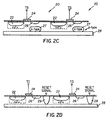
- FIG. 2C shows a row of the pixels as illustrated in FIG. 2A wherein the reset drains 27 are connected together by a patterned buried layer 28.
- FIG. 2P shows a row of pixels as illustrated in FIG. 2B wherein the reset drains 29 are connected together by a patterned buried layer 28.
- the SIG 6, RSG 9 and ROWST 8 have been omitted for simplicity of drawing.
Landscapes
- Solid State Image Pick-Up Elements (AREA)
- Transforming Light Signals Into Electric Signals (AREA)
Applications Claiming Priority (4)
| Application Number | Priority Date | Filing Date | Title |
|---|---|---|---|
| US1812696P | 1996-05-22 | 1996-05-22 | |
| US18126 | 1996-05-22 | ||
| US08/806,370 US5872371A (en) | 1997-02-27 | 1997-02-27 | Active pixel sensor with punch-through reset and cross-talk suppression |
| US806370 | 1997-02-27 |
Publications (3)
| Publication Number | Publication Date |
|---|---|
| EP0809299A2 true EP0809299A2 (de) | 1997-11-26 |
| EP0809299A3 EP0809299A3 (de) | 1998-09-02 |
| EP0809299B1 EP0809299B1 (de) | 2008-04-23 |
Family
ID=26690770
Family Applications (1)
| Application Number | Title | Priority Date | Filing Date |
|---|---|---|---|
| EP97201413A Expired - Lifetime EP0809299B1 (de) | 1996-05-22 | 1997-05-10 | Aktiver Pixelsensor mit Durchbruch-Rücksetzstruktur und Unterdrückung des Übersprechsignales |
Country Status (3)
| Country | Link |
|---|---|
| EP (1) | EP0809299B1 (de) |
| JP (1) | JP3892112B2 (de) |
| DE (1) | DE69738645T2 (de) |
Cited By (14)
| Publication number | Priority date | Publication date | Assignee | Title |
|---|---|---|---|---|
| GB2334817A (en) * | 1998-02-28 | 1999-09-01 | Hyundai Electronics Ind | Photodiodes for image sensors |
| EP0948056A2 (de) | 1998-03-19 | 1999-10-06 | Canon Kabushiki Kaisha | Festkörper-Bildaufnahmevorrichtung und deren Herstellungsverfahren |
| GB2339333A (en) * | 1998-06-29 | 2000-01-19 | Hyundai Electronics Ind | Photodiode having charge transfer function and image sensor using the same. |
| EP0978878A3 (de) * | 1998-07-01 | 2000-05-24 | InnoVision, Inc. | Festkörper-Bildaufnahmevorrichtung und Verfahren zum Erfassen eines optischen Signals mit Hilfe einer solchen Vorrichtung |
| EP1107315A1 (de) * | 1999-12-01 | 2001-06-13 | Innotech Corporation | Festkörper-Bildaufnahmeeinrichtung und Herstellungsverfahren dafür |
| WO2002029896A3 (en) * | 2000-10-05 | 2002-09-12 | Conexant Systems Inc | Cmos imager with discharge path to suppress reset noise |
| KR100377598B1 (ko) * | 2000-01-07 | 2003-03-29 | 이노텍 가부시기가이샤 | 고체 촬상 장치 및 그 구동 방법 |
| WO2007038107A3 (en) * | 2005-09-28 | 2007-10-04 | Eastman Kodak Co | Photodetector and n-layer structure for improved collection |
| WO2008073247A1 (en) * | 2006-12-11 | 2008-06-19 | Eastman Kodak Company | Two epitaxial layers with buried subcollector to reduce crosstalk in an image sensor |
| WO2008133787A1 (en) * | 2007-04-27 | 2008-11-06 | Aptina Imaging Corporation | Image sensor with improved quantum efficiency of red pixels and corresponding fabrication method |
| US7728277B2 (en) | 2005-11-16 | 2010-06-01 | Eastman Kodak Company | PMOS pixel structure with low cross talk for active pixel image sensors |
| US9093573B2 (en) | 2013-09-09 | 2015-07-28 | Semiconductor Components Industries, Llc | Image sensor including temperature sensor and electronic shutter function |
| US9574951B2 (en) | 2013-09-09 | 2017-02-21 | Semiconductor Components Industries, Llc | Image sensor including temperature sensor and electronic shutter function |
| EP3352220A4 (de) * | 2015-09-18 | 2019-08-07 | National University Corporation Shizuoka University | Halbleiterelement und festkörperbildaufnahmevorrichtung |
Families Citing this family (4)
| Publication number | Priority date | Publication date | Assignee | Title |
|---|---|---|---|---|
| US6587146B1 (en) * | 1998-11-20 | 2003-07-01 | Eastman Kodak Company | Three transistor active pixel sensor architecture with correlated double sampling |
| JP2005039219A (ja) * | 2004-06-04 | 2005-02-10 | Canon Inc | 固体撮像装置 |
| WO2016141388A1 (en) * | 2015-03-05 | 2016-09-09 | Dartmouth College | Gateless reset for image sensor pixels |
| JP2018513570A (ja) * | 2015-03-31 | 2018-05-24 | ダートマス カレッジ | Jfetソースフォロアを有するイメージセンサ及びイメージセンサ画素 |
Family Cites Families (12)
| Publication number | Priority date | Publication date | Assignee | Title |
|---|---|---|---|---|
| JPS5373031A (en) * | 1976-12-13 | 1978-06-29 | Hitachi Ltd | Solid pickup device |
| US4580155A (en) * | 1982-12-21 | 1986-04-01 | Northern Telecom Limited | Deep depletion CCD imager |
| JPS60124180A (ja) * | 1983-12-09 | 1985-07-03 | Victor Co Of Japan Ltd | 固体撮像板及び撮像方式 |
| JPH0287573A (ja) * | 1988-09-22 | 1990-03-28 | Nec Corp | 固体撮像装置 |
| CA2056087C (en) * | 1990-11-27 | 1998-01-27 | Masakazu Morishita | Photoelectric converting device and information processing apparatus employing the same |
| JPH04373136A (ja) * | 1991-06-21 | 1992-12-25 | Nec Corp | 電荷結合装置 |
| JP3060649B2 (ja) * | 1991-10-04 | 2000-07-10 | 日本電気株式会社 | 半導体装置及びその駆動方法 |
| JP2950387B2 (ja) * | 1992-03-19 | 1999-09-20 | 日本電気株式会社 | 電荷結合装置 |
| JPH05328225A (ja) * | 1992-05-15 | 1993-12-10 | Sony Corp | 増幅型固体撮像装置 |
| US5338946A (en) * | 1993-01-08 | 1994-08-16 | Eastman Kodak Company | Solid state image sensor with fast reset |
| JP2875132B2 (ja) * | 1993-02-25 | 1999-03-24 | シャープ株式会社 | 電荷転送装置 |
| JPH07106553A (ja) * | 1993-10-06 | 1995-04-21 | Nec Corp | 固体撮像素子 |
-
1997
- 1997-05-10 DE DE69738645T patent/DE69738645T2/de not_active Expired - Lifetime
- 1997-05-10 EP EP97201413A patent/EP0809299B1/de not_active Expired - Lifetime
- 1997-05-21 JP JP13133197A patent/JP3892112B2/ja not_active Expired - Lifetime
Cited By (32)
| Publication number | Priority date | Publication date | Assignee | Title |
|---|---|---|---|---|
| US6512547B1 (en) | 1998-01-07 | 2003-01-28 | Innovision, Inc. | Solid-state imaging device and method of detecting optical signals using the same |
| CN100377362C (zh) * | 1998-02-28 | 2008-03-26 | 美格纳半导体有限会社 | 图像传感器件及制造方法 |
| GB2334817B (en) * | 1998-02-28 | 2003-07-30 | Hyundai Electronics Ind | Photodiode for use in a CMOS image sensor and method for fabricating the same |
| GB2334817A (en) * | 1998-02-28 | 1999-09-01 | Hyundai Electronics Ind | Photodiodes for image sensors |
| US7274394B2 (en) | 1998-03-19 | 2007-09-25 | Canon Kabushiki Kaisha | Solid state image pickup device and manufacturing method therefor |
| US9257479B2 (en) | 1998-03-19 | 2016-02-09 | Canon Kabushiki Kaisha | Solid state image pickup device and manufacturing method therefor |
| EP0948056A3 (de) * | 1998-03-19 | 2000-02-23 | Canon Kabushiki Kaisha | Festkörper-Bildaufnahmevorrichtung und deren Herstellungsverfahren |
| US6661459B1 (en) | 1998-03-19 | 2003-12-09 | Canon Kabushiki Kaisha | Solid state image pickup device with LDD structure and reset transistor |
| US7705373B2 (en) | 1998-03-19 | 2010-04-27 | Canon Kabushiki Kaisha | Solid state image pickup device and manufacturing method therefor |
| US8395193B2 (en) | 1998-03-19 | 2013-03-12 | Canon Kabushiki Kaisha | Solid state image pickup device and manufacturing method therefor |
| EP0948056A2 (de) | 1998-03-19 | 1999-10-06 | Canon Kabushiki Kaisha | Festkörper-Bildaufnahmevorrichtung und deren Herstellungsverfahren |
| US8138528B2 (en) | 1998-03-19 | 2012-03-20 | Canon Kabushiki Kaisha | Solid state image pickup device and manufacturing method therefor |
| GB2339333B (en) * | 1998-06-29 | 2003-07-09 | Hyundai Electronics Ind | Photodiode having charge function and image sensor using the same |
| GB2339333A (en) * | 1998-06-29 | 2000-01-19 | Hyundai Electronics Ind | Photodiode having charge transfer function and image sensor using the same. |
| EP0978878A3 (de) * | 1998-07-01 | 2000-05-24 | InnoVision, Inc. | Festkörper-Bildaufnahmevorrichtung und Verfahren zum Erfassen eines optischen Signals mit Hilfe einer solchen Vorrichtung |
| EP1107315A1 (de) * | 1999-12-01 | 2001-06-13 | Innotech Corporation | Festkörper-Bildaufnahmeeinrichtung und Herstellungsverfahren dafür |
| KR100377598B1 (ko) * | 2000-01-07 | 2003-03-29 | 이노텍 가부시기가이샤 | 고체 촬상 장치 및 그 구동 방법 |
| WO2002029896A3 (en) * | 2000-10-05 | 2002-09-12 | Conexant Systems Inc | Cmos imager with discharge path to suppress reset noise |
| WO2007038107A3 (en) * | 2005-09-28 | 2007-10-04 | Eastman Kodak Co | Photodetector and n-layer structure for improved collection |
| US7875916B2 (en) | 2005-09-28 | 2011-01-25 | Eastman Kodak Company | Photodetector and n-layer structure for improved collection efficiency |
| CN101273457B (zh) * | 2005-09-28 | 2011-11-16 | 全视技术有限公司 | 光电探测器和用来提高收集的n-层结构 |
| US7728277B2 (en) | 2005-11-16 | 2010-06-01 | Eastman Kodak Company | PMOS pixel structure with low cross talk for active pixel image sensors |
| US7776638B2 (en) | 2006-12-11 | 2010-08-17 | Eastman Kodak Company | Two epitaxial layers to reduce crosstalk in an image sensor |
| CN101558496B (zh) * | 2006-12-11 | 2011-09-14 | 全视技术有限公司 | 一种图像传感器及制造该图像传感器的方法 |
| WO2008073247A1 (en) * | 2006-12-11 | 2008-06-19 | Eastman Kodak Company | Two epitaxial layers with buried subcollector to reduce crosstalk in an image sensor |
| US7821046B2 (en) | 2007-04-27 | 2010-10-26 | Aptina Imaging Corporation | Methods, structures and sytems for an image sensor device for improving quantum efficiency of red pixels |
| WO2008133787A1 (en) * | 2007-04-27 | 2008-11-06 | Aptina Imaging Corporation | Image sensor with improved quantum efficiency of red pixels and corresponding fabrication method |
| US9093573B2 (en) | 2013-09-09 | 2015-07-28 | Semiconductor Components Industries, Llc | Image sensor including temperature sensor and electronic shutter function |
| US9574951B2 (en) | 2013-09-09 | 2017-02-21 | Semiconductor Components Industries, Llc | Image sensor including temperature sensor and electronic shutter function |
| US9835504B2 (en) | 2013-09-09 | 2017-12-05 | Semiconductor Components Industries, Llc | Image sensor including temperature sensor and electronic shutter function |
| EP3352220A4 (de) * | 2015-09-18 | 2019-08-07 | National University Corporation Shizuoka University | Halbleiterelement und festkörperbildaufnahmevorrichtung |
| US10453880B2 (en) | 2015-09-18 | 2019-10-22 | National University Corporation Shizuoka University | Semiconductor element and solid-state imaging device |
Also Published As
| Publication number | Publication date |
|---|---|
| EP0809299A3 (de) | 1998-09-02 |
| JP3892112B2 (ja) | 2007-03-14 |
| DE69738645T2 (de) | 2009-06-10 |
| JPH1070262A (ja) | 1998-03-10 |
| DE69738645D1 (de) | 2008-06-05 |
| EP0809299B1 (de) | 2008-04-23 |
Similar Documents
| Publication | Publication Date | Title |
|---|---|---|
| US5872371A (en) | Active pixel sensor with punch-through reset and cross-talk suppression | |
| US6326230B1 (en) | High speed CMOS imager with motion artifact supression and anti-blooming | |
| US9654713B2 (en) | Image sensors, methods, and pixels with tri-level biased transfer gates | |
| EP0854516B1 (de) | Photodiode vom Typ teilweise befestigende Schicht für Festkörperbildaufnahmevorrichtungen | |
| EP0809299B1 (de) | Aktiver Pixelsensor mit Durchbruch-Rücksetzstruktur und Unterdrückung des Übersprechsignales | |
| US6943838B2 (en) | Active pixel sensor pixel having a photodetector whose output is coupled to an output transistor gate | |
| US7105371B2 (en) | Method of acquiring an image from an optical structure having pixels with dedicated readout circuits | |
| JP3874135B2 (ja) | 固体撮像素子 | |
| EP0809300B1 (de) | Bildsensor mit aktiven Bildelementen mit Einzelbildrücksetzung | |
| US7265397B1 (en) | CCD imager constructed with CMOS fabrication techniques and back illuminated imager with improved light capture | |
| US6278142B1 (en) | Semiconductor image intensifier | |
| US7833814B2 (en) | Method of forming pinned photodiode (PPD) pixel with high shutter rejection ratio for snapshot operating CMOS sensor | |
| US7687302B2 (en) | Frame shutter pixel with an isolated storage node | |
| US6876019B2 (en) | Charge transfer apparatus | |
| JP3667220B2 (ja) | 固体撮像装置、撮像システム及び固体撮像装置の駆動方法 | |
| JPH08293591A (ja) | 光電変換素子及び光電変換装置 | |
| JP2003017677A (ja) | 撮像装置 | |
| JP3919243B2 (ja) | 光電変換装置 | |
| KR100801758B1 (ko) | 이미지 센서 및 그 제어 방법 | |
| JP2003169256A (ja) | 固体撮像装置 | |
| JPH0150156B2 (de) | ||
| Fossum et al. | Method of acquiring an image from an optical structure having pixels with dedicated readout circuits | |
| JPH03220770A (ja) | イメージ・センシング装置 | |
| JPH0463591B2 (de) |
Legal Events
| Date | Code | Title | Description |
|---|---|---|---|
| PUAI | Public reference made under article 153(3) epc to a published international application that has entered the european phase |
Free format text: ORIGINAL CODE: 0009012 |
|
| AK | Designated contracting states |
Kind code of ref document: A2 Designated state(s): DE FR GB IT |
|
| PUAL | Search report despatched |
Free format text: ORIGINAL CODE: 0009013 |
|
| AK | Designated contracting states |
Kind code of ref document: A3 Designated state(s): DE FR GB IT |
|
| 17P | Request for examination filed |
Effective date: 19990226 |
|
| 17Q | First examination report despatched |
Effective date: 20051110 |
|
| GRAP | Despatch of communication of intention to grant a patent |
Free format text: ORIGINAL CODE: EPIDOSNIGR1 |
|
| GRAS | Grant fee paid |
Free format text: ORIGINAL CODE: EPIDOSNIGR3 |
|
| GRAA | (expected) grant |
Free format text: ORIGINAL CODE: 0009210 |
|
| AK | Designated contracting states |
Kind code of ref document: B1 Designated state(s): DE FR GB IT |
|
| REG | Reference to a national code |
Ref country code: GB Ref legal event code: FG4D |
|
| REF | Corresponds to: |
Ref document number: 69738645 Country of ref document: DE Date of ref document: 20080605 Kind code of ref document: P |
|
| ET | Fr: translation filed | ||
| PLBE | No opposition filed within time limit |
Free format text: ORIGINAL CODE: 0009261 |
|
| STAA | Information on the status of an ep patent application or granted ep patent |
Free format text: STATUS: NO OPPOSITION FILED WITHIN TIME LIMIT |
|
| 26N | No opposition filed |
Effective date: 20090126 |
|
| PGFP | Annual fee paid to national office [announced via postgrant information from national office to epo] |
Ref country code: GB Payment date: 20090407 Year of fee payment: 13 |
|
| GBPC | Gb: european patent ceased through non-payment of renewal fee |
Effective date: 20100510 |
|
| PG25 | Lapsed in a contracting state [announced via postgrant information from national office to epo] |
Ref country code: GB Free format text: LAPSE BECAUSE OF NON-PAYMENT OF DUE FEES Effective date: 20100510 |
|
| REG | Reference to a national code |
Ref country code: FR Ref legal event code: TP Owner name: OMNI VISION TECHNOLOGIES, INC., US Effective date: 20110829 |
|
| REG | Reference to a national code |
Ref country code: FR Ref legal event code: PLFP Year of fee payment: 20 |
|
| PGFP | Annual fee paid to national office [announced via postgrant information from national office to epo] |
Ref country code: DE Payment date: 20160524 Year of fee payment: 20 |
|
| PGFP | Annual fee paid to national office [announced via postgrant information from national office to epo] |
Ref country code: FR Payment date: 20160428 Year of fee payment: 20 Ref country code: IT Payment date: 20160517 Year of fee payment: 20 |
|
| REG | Reference to a national code |
Ref country code: DE Ref legal event code: R071 Ref document number: 69738645 Country of ref document: DE |