EP0809280A2 - Verfahren zur Herstellung einer Vorrichtung auf der Basis von InP mittels Wachstum von Halbleiter auf einer nicht planen Oberfläche - Google Patents
Verfahren zur Herstellung einer Vorrichtung auf der Basis von InP mittels Wachstum von Halbleiter auf einer nicht planen Oberfläche Download PDFInfo
- Publication number
- EP0809280A2 EP0809280A2 EP97303256A EP97303256A EP0809280A2 EP 0809280 A2 EP0809280 A2 EP 0809280A2 EP 97303256 A EP97303256 A EP 97303256A EP 97303256 A EP97303256 A EP 97303256A EP 0809280 A2 EP0809280 A2 EP 0809280A2
- Authority
- EP
- European Patent Office
- Prior art keywords
- phosphorus
- growth
- inp
- mass
- semiconductor
- Prior art date
- Legal status (The legal status is an assumption and is not a legal conclusion. Google has not performed a legal analysis and makes no representation as to the accuracy of the status listed.)
- Withdrawn
Links
Images


Classifications
-
- H10P14/2909—
-
- H10P14/2925—
-
- H10P14/3218—
-
- H10P14/3221—
-
- H10P14/3251—
-
- H10P14/3418—
-
- H10P14/3421—
Definitions
- This invention pertains to making InP-based distributed feedback (DFB) lasers and other InP-based semiconductor devices.
- DFB distributed feedback
- DFB lasers typically comprise a "grating" that serves to determine and stabilize the laser wavelength.
- the grating exemplarily is formed by a process that involves deposition of a conventional resist layer on the surface of a III/V semiconductor wafer, patterning of the resist layer, and etching of the exposed portions of the semiconductor surface. After removal of the resist, III/V semiconductor material of desired composition and thickness is deposited on the thus created "corrugated" semiconductor surface, and laser manufacture is completed.
- the grating can be disposed below or above the active layer of the laser.
- any significant wafer-to-wafer (or chip-to-chip) variation in the grating profile and/or spacing results in undesirable variations in coupling coefficiency, frequently negatively impacting device yield.
- the growth of semiconductor material on a corrugated semiconductor surface is an example of a wider processing task, namely, the growth of compound semiconductor material on a non-planar semiconductor surface.
- the need for such growth arises, for instance, in the manufacture of some photonic and electronic devices or integrated circuits, e.g., in the manufacture of lasers integrated with modulators.
- the method that is disclosed herein can advantageously be used in the manufacture of a variety of InP-based semiconductor devices involving growth of compound semiconductor material on a non-planar substrate, the method will be described below in terms of a specific and important embodiment, namely, the manufacture of InP-based DFB lasers involving the growth of ternary or quaternary III/V semiconductor material such as GaInAsP on a corrugated InP surface, or the growth of InP on a corrugated ternary or quaternary III/V semiconductor (e.g., GaInAsP) surface.
- ternary or quaternary III/V semiconductor material such as GaInAsP on a corrugated InP surface
- GaInAsP ternary or quaternary III/V semiconductor
- an “InP-based” device we mean a III/V semiconductor device formed by epitaxial growth on an InP substrate, or containing one or more layers of InP.
- the invention is defined by the claims. In a broad aspect it is embodied in a method of making an InP-based semiconductor device that involves heteroepitaxial growth of III/V semiconductor material on a non-planar III/V semiconductor surface.
- the method comprises providing an InP-based semiconductor body having a major surface, patterning the surface such that a surface with non-planar surface features results, and growing a phosphorus (P)-containing semiconductor material (e.g., GaInAsP or InP) on the patterned major surface. Subsequently one or more further steps (e.g., growth of one or more further layers of semiconductor material, metal deposition, heat treatment, cleaving, packaging, etc.) towards completion of the semiconductor device are carried out.
- P phosphorus
- the method comprises heating, in a substantially evacuated (background pressure typically ⁇ 10 -8 Torr) chamber, the semiconductor body with the non-planar surface features to a mass-transport temperature, and exposing, in the substantially evacuated chamber, the patterned major surface to a flux of at least phosphorus from a solid phosphorus flux source for a time effective for providing a shape change of the non-planar surface features by mass-transport; and furthermore comprises carrying out at least an initial portion of the growth step without exposing the semiconductor body to an ambient atmosphere, with the semiconductor body preferably being at a growth temperature that does not exceed said mass-transport temperature at least during said initial portion.
- a substantially evacuated background pressure typically ⁇ 10 -8 Torr
- a significant feature of the method is the use of solid sources of P and, optionally, As, rather than the commonly used H-containing compounds of P and As (e.g., phosphene and arsine). This facilitates use of lower process temperatures, which in turn can result in less dopant diffusion and a more reproducible process, and thus in higher device yield.
- solid sources of P and, optionally, As rather than the commonly used H-containing compounds of P and As (e.g., phosphene and arsine).
- Exposure of the surface to As during the mass transport step generally decreases the rate of mass transport (and thus of shape change), as compared to the rate when the surface is exposed to P only.
- the ratio of As flux to P flux thus will generally be selected to result in a desired rate of mass transport. Since this rate also depends on the temperature of the body, no general rule can be given. However, a minor amount of experimentation will generally suffice to determine a satisfactory ratio at any given temperature.
- Exemplary and technologically important devices that are advantageously made by the inventive method are InP-based 1.3 ⁇ m and 1.55 ⁇ m DFB lasers.
- Such lasers find widespread use in, for instance, optical fiber communication systems.
- Manufacture of such lasers exemplarily requires growth of GaInAsP on a corrugated crystal (exemplarily InP) surface.
- a corrugated crystal exemplarily InP
- GaInAsP we mean Ga 1-x In x As 1-y P y , with both x and y between 0 and 1.
- x and y are selected in known manner such that the GaInAsP is substantially lattice matched to InP, but use of non-lattice-matched GaInAsP is not precluded.
- the lasers can be produced in conventional fashion, except that the inventive method of making the grating and growing semiconductor material thereon is substituted for any of the prior art methods. Since the conventional manufacturing steps are well known to those skilled in the art they do not require detailed recitation.
- the inventive method can be practiced in known equipment, provided that the evacuable growth chamber comprises means for producing a phosphorus (P) flux (and typically also an arsenic (As) flux) from a solid source.
- P phosphorus
- As arsenic
- grating modification and semiconductor growth in a commercially available (Riber 2300) MBE system that comprises a Riber model KPC 40 valved phosphorus cell (having three separately controllable temperature zones) and a third generation EPI model RB500VAs valved arsenic cell (having two temperature zones).
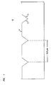
- FIG. 1 substantially reproduces relevant features of a cross-sectional TEM micrograph of an exemplary grating 10 etched into a (100) surface 11 of an InP wafer.
- the grating periodicity was 0.20 ⁇ m, the grooves were oriented parallel to the [011] direction, had (111)A side walls 12 and were about 60nm deep.
- the grating was produced in conventional fashion, using holographic photolithography to pattern a conventional resist layer, followed by conventional wet chemical etching.
- the as-etched grating exhibits steep sidewalls and sharp corners. It is known that such features frequently cause strong localized composition shifts, which, in turn, can introduce large lattice strains.
- the grating profile desirably is smoothed, typically by thermally activated atom migration, prior to the initiation of overgrowth. This smoothing of the sharp grating features is referred to as mass transport, and we will herein use this terminology, regardless of the actual mechanism involved.
- FIG. 2 is a cross-sectional scanning electron micrograph of an InP grating 20 after heating of a grating as shown in Fig. 1 at 480°C for 5 minutes under a phosphorus flux (from a solid source) of 4x10 -6 Torr.
- the rounding of the sharp features is obvious.
- Grating depth was reduced to about 30 nm. Heating for periods longer than 5 minutes did not result in any significant further reduction of grating depth, but heating at 510°C for 20 minutes substantially removed the grating.
- the mass transport rate is also a function of the phosphorus flux, in addition to being a function of temperature. Higher phosphorus flux can reduce the mass transport rate.
- appropriate mass transport temperatures may be somewhat different. Suitable mass transport temperatures are readily determined by minor experimentation.
- mass transport according to the invention typically occurs at substantially lower temperatures than does mass transport in the conventional (MOCVD) method.
- the latter typically occurs at temperatures above about 600°C. This difference of mass transport temperatures has implications for reproducibility and thus manufacturability, with lower temperatures generally providing better reproducibility.
- the mass transport treatment according to the invention results in thermal oxide desorption, and generally in generation of a substantially atomically clean surface.
- This is an important aspect of the inventive method which facilitates deposition of high quality overlayer material, provided the pristine surface condition is maintained up to coverage of the surface with overlayer material. This will be the case if the vacuum is maintained in the growth chamber, and if the time between completion of mass transport and commencement is suitably short, exemplarily less than 10 minutes.
- FIG. 3 is a representation of a cross-sectional TEM micrograph of a InP grating as shown in FIG. 2, with GaInAsP material grown on corrugated surface 31 of InP body 30.
- 0.8 nm InP marker layers (321, 322, 323, 324) were provided between 17 nm GaInAsP layers 331-335. Such markers typically would not be present in DFB lasers or other devices.
- Deposition was commenced immediately (within about one minute) after completion of the mass-transport heat treatment (480°C, P-flux 4 x 10 -6 Torr, 5 minutes). The fluxes were selected to yield quaternary material with emission wavelength in the range 1.17-1.20 ⁇ m.
- Ga and In were provided by elemental sources in known manner. Initial growth was carried out at 480°C, followed by a ramp-up to the final growth temperature of 530°C. The final temperature was reached before deposition of the second marker layer. Growth rates were 1.33 ⁇ m/h for the GaInAsP, and 0.57 ⁇ m/h for InP. Layer 33 is an InP layer provided to facilitate the TEM measurements.
- the second marker layer is extremely smooth and already essentially planar, indicative of the ability of the inventive method to provide high quality planar overgrowth on a non-planar surface.
- a further InP grating with GaInAsP overgrowth was produced as described above, except that the final growth temperature was 500°C.
- the lower growth temperature resulted in overgrowth of somewhat lower quality, with the third marker layer not being completely planar.
- the final growth temperature is in the range 480-600°C, with temperatures above 500°C being preferred.
- Samples grown according to the invention were generally free of growth-related dislocations, with samples grown at 530°C generally exhibiting lower lattice strain than samples grown at 500°C.
- Photoluminescence (PL) measurements of GaInAsP grown on InP gratings and planar InP indicate that the quality of the former is comparable to that of the latter.
Landscapes
- Semiconductor Lasers (AREA)
- Chemical Vapour Deposition (AREA)
- Physical Deposition Of Substances That Are Components Of Semiconductor Devices (AREA)
- Led Devices (AREA)
Applications Claiming Priority (2)
| Application Number | Priority Date | Filing Date | Title |
|---|---|---|---|
| US08/652,285 US5633193A (en) | 1996-05-22 | 1996-05-22 | Method of making an InP-based device comprising semiconductor growth on a non-planar surface |
| US652285 | 1996-05-22 |
Publications (2)
| Publication Number | Publication Date |
|---|---|
| EP0809280A2 true EP0809280A2 (de) | 1997-11-26 |
| EP0809280A3 EP0809280A3 (de) | 2001-08-29 |
Family
ID=24616262
Family Applications (1)
| Application Number | Title | Priority Date | Filing Date |
|---|---|---|---|
| EP97303256A Withdrawn EP0809280A3 (de) | 1996-05-22 | 1997-05-13 | Verfahren zur Herstellung einer Vorrichtung auf der Basis von InP mittels Wachstum von Halbleiter auf einer nicht planen Oberfläche |
Country Status (4)
| Country | Link |
|---|---|
| US (1) | US5633193A (de) |
| EP (1) | EP0809280A3 (de) |
| JP (1) | JPH1065276A (de) |
| CA (1) | CA2200124C (de) |
Families Citing this family (7)
| Publication number | Priority date | Publication date | Assignee | Title |
|---|---|---|---|---|
| FR2765031B1 (fr) * | 1997-06-19 | 1999-09-24 | Alsthom Cge Alcatel | Controle de la profondeur de gravure dans la fabrication de composants semiconducteurs |
| US7058246B2 (en) * | 2001-10-09 | 2006-06-06 | Infinera Corporation | Transmitter photonic integrated circuit (TxPIC) chip with enhanced power and yield without on-chip amplification |
| TWI248691B (en) * | 2005-06-03 | 2006-02-01 | Formosa Epitaxy Inc | Light emitting diode and method of fabricating thereof |
| CN100423303C (zh) * | 2005-06-09 | 2008-10-01 | 璨圆光电股份有限公司 | 发光二极管及其制造方法 |
| JP4951267B2 (ja) * | 2006-04-27 | 2012-06-13 | 日本オプネクスト株式会社 | 半導体レーザ素子の製造方法 |
| US7645624B2 (en) * | 2007-10-31 | 2010-01-12 | Tekcore Co., Ltd. | Method for self bonding epitaxy |
| JP5409170B2 (ja) * | 2009-07-30 | 2014-02-05 | キヤノン株式会社 | 半導体素子の製造方法および半導体素子 |
Family Cites Families (8)
| Publication number | Priority date | Publication date | Assignee | Title |
|---|---|---|---|---|
| JPS6079788A (ja) * | 1983-10-06 | 1985-05-07 | Nec Corp | 光双安定素子 |
| US4885262A (en) * | 1989-03-08 | 1989-12-05 | Intel Corporation | Chemical modification of spin-on glass for improved performance in IC fabrication |
| JPH02264491A (ja) * | 1989-04-04 | 1990-10-29 | Mitsubishi Electric Corp | 分布帰還型半導体レーザの製造方法 |
| US5126281A (en) * | 1990-09-11 | 1992-06-30 | Hewlett-Packard Company | Diffusion using a solid state source |
| US5387546A (en) * | 1992-06-22 | 1995-02-07 | Canon Sales Co., Inc. | Method for manufacturing a semiconductor device |
| EP0582986B1 (de) * | 1992-08-10 | 1999-01-20 | Canon Kabushiki Kaisha | Halbleitervorrichtung und Herstellungsverfahren |
| US5360763A (en) * | 1992-09-07 | 1994-11-01 | Nec Corporation | Method for fabricating an optical semiconductor device |
| US5399521A (en) * | 1993-10-08 | 1995-03-21 | Texas Instruments Incorporated | Method of semiconductor layer growth by MBE |
-
1996
- 1996-05-22 US US08/652,285 patent/US5633193A/en not_active Expired - Lifetime
-
1997
- 1997-03-17 CA CA002200124A patent/CA2200124C/en not_active Expired - Fee Related
- 1997-04-08 JP JP8901497A patent/JPH1065276A/ja active Pending
- 1997-05-13 EP EP97303256A patent/EP0809280A3/de not_active Withdrawn
Also Published As
| Publication number | Publication date |
|---|---|
| EP0809280A3 (de) | 2001-08-29 |
| JPH1065276A (ja) | 1998-03-06 |
| CA2200124C (en) | 2000-04-18 |
| CA2200124A1 (en) | 1997-11-22 |
| US5633193A (en) | 1997-05-27 |
Similar Documents
| Publication | Publication Date | Title |
|---|---|---|
| EP0665578B1 (de) | Halbleiterstruktur und Herstellungsverfahren | |
| US5633193A (en) | Method of making an InP-based device comprising semiconductor growth on a non-planar surface | |
| KR19990042070A (ko) | 고품위 지에이에이에스(GaAs) 양자점의 성장방법 | |
| US7704861B2 (en) | Electron beam microprocessing method | |
| Lee et al. | In 0.5 Ga 0.5 As quantum dot intermixing and evaporation in GaAs capping layer growth | |
| JP4651759B2 (ja) | 量子ドットを備えた素子 | |
| EP0618610A2 (de) | Verfahren zur Herstellung einer Verbundhalbleitervorrichtung | |
| Sakata et al. | Selective MOVPE growth of InGaAsP and InGaAs using TBA and TBP | |
| Heinecke et al. | Selective-area growth of III/V semiconductors in chemical beam epitaxy | |
| JP7287495B2 (ja) | 半導体層の形成方法 | |
| Araki et al. | Fabrication of InGaAs quantum wires and dots by selective molecular beam epitaxial growth on various mesa-patterned (001) InP substrates | |
| KR100359739B1 (ko) | 이종 단결정박막의 접합 및 덧성장방법 | |
| Panepucci et al. | Fabrication of InP/InGaAs quantum wires by free Cl2 | |
| JP2794506B2 (ja) | 化合物半導体ヘテロエピタキシャル成長方法 | |
| EP0590870A2 (de) | Herstellungsverfahren eines vergrabenen Heterostrukturlasers | |
| GB2411520A (en) | Method of forming laser mesa by reactive ion etching followed by in situ etching in regrowth reactor | |
| JP3529475B2 (ja) | 半導体微小ドットの製造方法 | |
| WO2005022640A1 (ja) | 半導体量子ドット素子及びその製造方法 | |
| JP3314794B2 (ja) | 半導体レーザおよびその製造方法 | |
| JP4041887B2 (ja) | アンチモン系量子ドットの形成方法 | |
| Temmyo et al. | Self-organization phenomenon of strained InGaAs on InP (311) substrates grown by metalorganic vapor phase epitaxy | |
| Kim et al. | Realization of Vertically Stacked InGaAs/GaAs Quantum Wires on V‐grooves with (322) Facet Sidewalls by Chemical Beam Epitaxy | |
| JPH10289997A (ja) | 半導体量子構造およびその製造方法 | |
| JPH0444414B2 (de) | ||
| Hwang et al. | The Growth of High Quality GaAs Epilayers on Stripe Patterned InP Substrates With a Transferred GaAs Fused Layer |
Legal Events
| Date | Code | Title | Description |
|---|---|---|---|
| PUAI | Public reference made under article 153(3) epc to a published international application that has entered the european phase |
Free format text: ORIGINAL CODE: 0009012 |
|
| AK | Designated contracting states |
Kind code of ref document: A2 Designated state(s): DE FR GB |
|
| PUAL | Search report despatched |
Free format text: ORIGINAL CODE: 0009013 |
|
| RAP1 | Party data changed (applicant data changed or rights of an application transferred) |
Owner name: AGERE SYSTEMS OPTOELECTRONICS GUARDIAN CORPORATION |
|
| AK | Designated contracting states |
Kind code of ref document: A3 Designated state(s): DE FR GB |
|
| RIC1 | Information provided on ipc code assigned before grant |
Free format text: 7H 01L 21/20 A, 7H 01L 33/00 B, 7H 01S 3/19 B |
|
| STAA | Information on the status of an ep patent application or granted ep patent |
Free format text: STATUS: THE APPLICATION IS DEEMED TO BE WITHDRAWN |
|
| 18D | Application deemed to be withdrawn |
Effective date: 20020301 |