EP0808230B1 - Polissage chimique-mecanique d'articles minces faisant appel a une technique de polissage pulse - Google Patents
Polissage chimique-mecanique d'articles minces faisant appel a une technique de polissage pulse Download PDFInfo
- Publication number
- EP0808230B1 EP0808230B1 EP96902098A EP96902098A EP0808230B1 EP 0808230 B1 EP0808230 B1 EP 0808230B1 EP 96902098 A EP96902098 A EP 96902098A EP 96902098 A EP96902098 A EP 96902098A EP 0808230 B1 EP0808230 B1 EP 0808230B1
- Authority
- EP
- European Patent Office
- Prior art keywords
- pressure
- wafer
- polishing
- chemical
- cmp
- Prior art date
- Legal status (The legal status is an assumption and is not a legal conclusion. Google has not performed a legal analysis and makes no representation as to the accuracy of the status listed.)
- Expired - Lifetime
Links
Images

Classifications
-
- B—PERFORMING OPERATIONS; TRANSPORTING
- B24—GRINDING; POLISHING
- B24B—MACHINES, DEVICES, OR PROCESSES FOR GRINDING OR POLISHING; DRESSING OR CONDITIONING OF ABRADING SURFACES; FEEDING OF GRINDING, POLISHING, OR LAPPING AGENTS
- B24B37/00—Lapping machines or devices; Accessories
- B24B37/04—Lapping machines or devices; Accessories designed for working plane surfaces
- B24B37/042—Lapping machines or devices; Accessories designed for working plane surfaces operating processes therefor
-
- B—PERFORMING OPERATIONS; TRANSPORTING
- B24—GRINDING; POLISHING
- B24B—MACHINES, DEVICES, OR PROCESSES FOR GRINDING OR POLISHING; DRESSING OR CONDITIONING OF ABRADING SURFACES; FEEDING OF GRINDING, POLISHING, OR LAPPING AGENTS
- B24B37/00—Lapping machines or devices; Accessories
- B24B37/04—Lapping machines or devices; Accessories designed for working plane surfaces
- B24B37/07—Lapping machines or devices; Accessories designed for working plane surfaces characterised by the movement of the work or lapping tool
- B24B37/10—Lapping machines or devices; Accessories designed for working plane surfaces characterised by the movement of the work or lapping tool for single side lapping
-
- H10P52/00—
Definitions
- the present invention relates a chemical-mechanical polishing method to effect a high removal rate of material and uniform planarization of a surface on a wafer during the manufacture of a semiconductor device.
- the invention has particularly application in rapidly planarizing thin films of dielectric material.
- Semiconductor integrated circuits are manufactured by forming an array of separate dies on a common semiconductor wafer. During processing, the wafer is treated to form specified regions of insulating, conductive and semiconductor type materials.
- a wiring pattern comprising a dense array of conductive lines is formed by depositing a metal layer and etching to form a conductive pattern.
- a dielectric is then applied to the wiring pattern and planarization is effected as by chemical-mechanical polishing.
- Chemical-mechanical polishing is a conventional technique employed to planarize a patterned insulating layer or a patterned metallic layer.
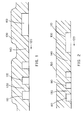
- a pattern 110 is formed on layer 120 of, for example, an insulating material, a conductive material such as a metal, or a semiconductor substrate having an interwiring spacing 130 and trench 140.
- the object is to completely fill the interwiring spacing 130 and trench 140 with a subsequently deposited material 100 as, for example, an insulating material if pattern 110 is a conductive pattern.
- layer 100 After layer 100 is deposited, it must be planarized to obtain a uniformly planarized surface 150 as shown in Fig. 2 wherein line numerals denote like components.
- Planarization is conventionally effected by plasma etching, or by a simplified faster and relatively inexpensive method known as chemicalmechanical planarization or polishing (CMP).
- CMP as defined in the preamble of claim 1 is a conventional technique as disclosed in, see for example, Salugsugan , U.S. Patent No. 5,245,794; Beyer et al. , U.S. Patent No. 4,944,836; Youmans, U.S. Patent No. 3,911,562. See also U.S. Patent No. 4,193,226 and 4,811,522 to Gill, Jr. and U.S. Patent No. 3,841,031 to Walsh which relate to CMP apparatus.
- wafers to be polished are mounted on polishing blocks which are placed on the CMP machine.
- a polishing pad is adapted to engage the wafers carried by the polishing blocks.
- a cleaning agent is dripped onto the pad continuously during the polishing operation while pressure is applied to the wafer.
- a typical CMP apparatus 300 is shown in Fig. 3 and comprises a rotatable polishing platen 302, polishing pad 304 mounted on platen 302, which are driven by microprocessor control motor (not shown) to spin at about 25 to about 50 RPM.
- Wafer 306 is mounted on the bottom of a rotatable polishing head 308 so that a major surface of wafer 306 to be polished is positionable to contact the underlying polish pad 304.
- Wafer 306 and polishing head 308 are attached to a vertical spindle 310 which is rotatably mounted in a lateral robotic arm 312 which rotates the polishing head 308 at about 15 to about 30 RPM in the same direction as platen 302 and radially positions the polishing head.
- Robotic arm 312 also vertically positions polishing head 308 to bring wafer 306 into contact with polishing head 304 and maintain an appropriate polishing contact pressure.
- a tube 314 opposite polishing head 308 above polishing pad 304 dispenses and evenly saturates the pad with an appropriate cleaning agent 316, typically a slurry.
- An object of the present invention is a CMP method for uniformly planarizing a surface on a wafer at a high removal rate of material.
- a method of manufacturing a semiconductor device wherein a surface on a wafer is planarized comprising: placing the wafer to be planarized on a polishing pad; applying a cleaning agent to the polishing pad; chemical-mechanical polishing the surface to effect planarization while applying a first pressure to the wafer; and intermittently reducing the first pressure to a second pressure a plurality of times during the course of chemical-mechanical polishing, whereby the pulsing pressure thereby created prevents starvation areas having insufficient cleaning agent on the wafer.
- Figure 1 illustrate a layer of material deposited on a patterned material.
- Figure 2 illustrates the planarized deposited layer of Figure 1.
- Figure 3 schematically illustrates a typical chemical-mechanical polishing machine.
- the present invention addresses the limitations of conventional CMP technology in achieving uniformly planarized surfaces of materials, particularly dielectric materials, at high removal rates.
- the inability of conventional CMP technology to achieve high polishing rates constitutes a serious economic impediment.
- Time consuming CMP decreases production throughput, consumes man hours and exhausts large amounts of cleaning agent and other consumable materials.
- the lack of a uniformly planarized surface adversely affects the reliability of the resulting semiconductor device, particularly in devices comprising multi-level vias wherein the upper vias would be overetched to insure complete etching at the lower levels.
- the present invention addresses and solves such limitations of conventional CMP technology, i.e., methodology and apparatus, by selecting an appropriate initial pressure applied to wafer undergoing CMP and intermittently reducing the initial pressure to a second pressure a plurality of times during the course of CMP processing. I discovered that during the course of CMP processing, the surface to be polished in contact with the polishing pad becomes depleted in cleaning agent, which adversely affects the polishing rate and uniformity of the CMP operation, since incomplete polishing occurs in depleted areas, as toward the center of the wafer.
- the initial pressure applied to the wafer undergoing CMP is intermittently reduced creating a pulsing pressure, thereby enabling the cleaning agent, which is normally continuously applied to the polishing pad, to continuously reach all portions of the surface of the wafer undergoing polishing throughout the entire CMP operation.
- the periodic reduction of pressure applied to the wafer during CMP processing eliminates the negative impact of starvation areas, i.e., areas which do not have a sufficient amount of cleaning agent.
- the present invention can be practiced employing otherwise conventional CMP technology, i.e., techniques and apparatus.
- CMP apparatus disclosed in the previously mentioned Gill, Jr . or Walsh patents can be employed in the practice of the present invention.
- a commercially available CMP apparatus which can be employed in the present invention is Model 372 Polish and manufactured by Westex Systems, Inc., of Phoenix, Arizona or Strasbaug, San Luis Opisbo, California Model 6DFSP form.
- the polishing pad employed in the claimed invention can be any of those which are conventionally employed in CMP, such as those comprising a cellular polyurethane pad, preferably about 50 mills thick.
- the cleaning agent employed in the claimed invention can be any of those conventionally employed in CMP processing.
- a slurry most preferably a slurry comprising potassium hydroxide and particulate silica, is employed.
- an optimum initial pressure is selected to obtain effective removal of material at an economically desirable high rate of speed, typically between about 6 and about 9 psi.
- the second or reduced pressure is generally less than about 2 psi, preferably less than about 1 psi, preferably about 0 psi.
- the polishing speed or rotations of the polishing pad is generally between about 20 and about 50 RPM.
- the improved CMP technique of the present invention can be employed to planarize various types of surfaces on a wafer, including conductive and insulating materials, such as oxides, tetraethyl orthosilicate, also referred to as tetraethoxysilane (TEOS), nitrides, polysilicon, single crystalline silicon, amorphous silicon, and mixtures thereof.
- conductive and insulating materials such as oxides, tetraethyl orthosilicate, also referred to as tetraethoxysilane (TEOS), nitrides, polysilicon, single crystalline silicon, amorphous silicon, and mixtures thereof.
- a dielectric layer such as TEOS
- the substrate of the wafer containing the conductive or non-conductive material is generally a semiconductor material, such as silicon.
- the first pressure is intermittently reduced to the second pressure during the course of CMP.
- the frequency of reducing the initial pressure depends upon each particular CMP operation, e.g., the particular CMP apparatus, speed of polishing, materials undergoing planarization and cleaning agent.
- the first pressure is reduced to the second pressure about every 1 to 15 seconds, preferably about every 1 to 10 seconds, most preferably about every 1 to 5 seconds.
- the first pressure is intermittently reduced to the second pressure about every 1 to 3 seconds.
- the speed and uniformity of planarization effected by conventional CMP technology is greatly improved by virtue intermittently reducing the pressure applied to the wafer undergoing planarization from an optimum initial pressure, preferably to about 0 psi.
- the inventive pulse CMP technique is applicable to a wide variety of situations which require planarization during the course of manufacturing a semiconductor device.
Landscapes
- Engineering & Computer Science (AREA)
- Mechanical Engineering (AREA)
- Mechanical Treatment Of Semiconductor (AREA)
- Finish Polishing, Edge Sharpening, And Grinding By Specific Grinding Devices (AREA)
Claims (17)
- Procédé de fabrication d'un dispositif à semi-conducteur dans lequel une surface d'une plaquette (306) est aplanie, consistant à :la première pression est réduite par intermittence afin d'exercer plusieurs fois une seconde pression au cours du polissage chimique-mécanique, de sorte que la pression à impulsion générée de ce fait empêche la formation de zones de manque présentant une quantité insuffisante d'agent nettoyant sur la plaquette (306).placer la plaquette (306) à aplanir sur un disque de polissage (304) ;appliquer un agent nettoyant sur le disque de polissage (304) ;effectuer un polissage chimique-mécanique de la surface pour réaliser l'aplanissement tout en appliquant une première pression sur la plaquette (306) ; caractérisé en ce que
- Procédé selon la revendication 1, dans lequel la première pression est de 41 à 62 kPa (6 à 9 psi) et la seconde pression est inférieure à 13,8 kPa (2 psi).
- Procédé selon la revendication 2, dans lequel la seconde pression est inférieure à 6,9 kPa (1 psi).
- Procédé selon la revendication 3, dans lequel la seconde pression est 0 kPa (0 psi).
- Procédé selon l'une quelconque des revendications précédentes, dans lequel la surface de la plaquette (306) comprend un matériau isolant.
- Procédé selon la revendication 5, dans lequel le matériau isolant est sélectionné dans le groupe constitué d'un oxyde, d'un nitrure, et de leurs mélanges.
- Procédé selon la revendication 6, dans lequel le matériau isolant est le TEOS (tétraéthoxysilane).
- Procédé selon la revendication 6, dans lequel le matériau isolant est de l'oxyde de silicium.
- Procédé selon l'une quelconque des revendications précédentes, dans lequel la surface de la plaquette (306) comprend un matériau sélectionné dans le groupe constitué d'un oxyde, d'un nitrure, de polysilicium, de silicium monocristallin, de silicium amorphe et de leurs mélanges.
- Procédé selon l'une quelconque des revendications précédentes dans lequel le substrat comprend du silicium.
- Procédé selon l'une quelconque des revendications précédentes, dans lequel la première pression est réduite par intermittence à la seconde pression toutes les 1 à 15 secondes environ pendant le polissage chimique-mécanique.
- Procédé selon la revendication 11, dans lequel la première pression est réduite par intermittence à la seconde pression toutes les 1 à 10 secondes environ.
- Procédé selon la revendication 12, dans lequel la première pression est réduite par intermittence à la seconde pression toutes les 1 à 5 secondes environ.
- Procédé selon la revendication 13, dans lequel la première pression est réduite par intermittence à la seconde pression toutes les 1 à 3 secondes environ.
- Procédé selon l'une quelconque des revendications précédentes, dans lequel le disque de polissage (304) comporte un polymère à fibres.
- Procédé selon l'une quelconque des revendications précédentes, dans lequel l'agent nettoyant comporte une suspension.
- Procédé selon la revendication 16, dans lequel la suspension comporte de l'hydroxyde de potassium et de la silice spéciale.
Applications Claiming Priority (3)
| Application Number | Priority Date | Filing Date | Title |
|---|---|---|---|
| US08/383,737 US5486265A (en) | 1995-02-06 | 1995-02-06 | Chemical-mechanical polishing of thin materials using a pulse polishing technique |
| US383737 | 1995-02-06 | ||
| PCT/US1996/000151 WO1996024466A1 (fr) | 1995-02-06 | 1996-01-11 | Polissage chimique-mecanique d'articles minces faisant appel a une technique de polissage pulse |
Publications (2)
| Publication Number | Publication Date |
|---|---|
| EP0808230A1 EP0808230A1 (fr) | 1997-11-26 |
| EP0808230B1 true EP0808230B1 (fr) | 2000-04-26 |
Family
ID=23514490
Family Applications (1)
| Application Number | Title | Priority Date | Filing Date |
|---|---|---|---|
| EP96902098A Expired - Lifetime EP0808230B1 (fr) | 1995-02-06 | 1996-01-11 | Polissage chimique-mecanique d'articles minces faisant appel a une technique de polissage pulse |
Country Status (6)
| Country | Link |
|---|---|
| US (1) | US5486265A (fr) |
| EP (1) | EP0808230B1 (fr) |
| JP (1) | JPH10513121A (fr) |
| KR (1) | KR100399877B1 (fr) |
| DE (1) | DE69607940T2 (fr) |
| WO (1) | WO1996024466A1 (fr) |
Families Citing this family (32)
| Publication number | Priority date | Publication date | Assignee | Title |
|---|---|---|---|---|
| US5688364A (en) * | 1994-12-22 | 1997-11-18 | Sony Corporation | Chemical-mechanical polishing method and apparatus using ultrasound applied to the carrier and platen |
| JPH08257902A (ja) * | 1995-03-28 | 1996-10-08 | Ebara Corp | ポリッシング装置 |
| US5665201A (en) * | 1995-06-06 | 1997-09-09 | Advanced Micro Devices, Inc. | High removal rate chemical-mechanical polishing |
| JP2850803B2 (ja) * | 1995-08-01 | 1999-01-27 | 信越半導体株式会社 | ウエーハ研磨方法 |
| JPH0955362A (ja) * | 1995-08-09 | 1997-02-25 | Cypress Semiconductor Corp | スクラッチを減少する集積回路の製造方法 |
| US5665202A (en) * | 1995-11-24 | 1997-09-09 | Motorola, Inc. | Multi-step planarization process using polishing at two different pad pressures |
| EP0779655A3 (fr) * | 1995-12-14 | 1997-07-16 | International Business Machines Corporation | Procédé pour le polissage chimique-mécanique d'un substrat d'un composant électronique |
| KR100241537B1 (ko) * | 1996-06-21 | 2000-02-01 | 김영환 | 반도체 소자의 층간 절연막 평탄화 방법 |
| US5968851A (en) * | 1997-03-19 | 1999-10-19 | Cypress Semiconductor Corp. | Controlled isotropic etch process and method of forming an opening in a dielectric layer |
| US6007411A (en) * | 1997-06-19 | 1999-12-28 | Interantional Business Machines Corporation | Wafer carrier for chemical mechanical polishing |
| US6139406A (en) | 1997-06-24 | 2000-10-31 | Applied Materials, Inc. | Combined slurry dispenser and rinse arm and method of operation |
| US6143663A (en) * | 1998-01-22 | 2000-11-07 | Cypress Semiconductor Corporation | Employing deionized water and an abrasive surface to polish a semiconductor topography |
| US6200896B1 (en) | 1998-01-22 | 2001-03-13 | Cypress Semiconductor Corporation | Employing an acidic liquid and an abrasive surface to polish a semiconductor topography |
| US6171180B1 (en) | 1998-03-31 | 2001-01-09 | Cypress Semiconductor Corporation | Planarizing a trench dielectric having an upper surface within a trench spaced below an adjacent polish stop surface |
| US6113465A (en) * | 1998-06-16 | 2000-09-05 | Speedfam-Ipec Corporation | Method and apparatus for improving die planarity and global uniformity of semiconductor wafers in a chemical mechanical polishing context |
| US6129610A (en) * | 1998-08-14 | 2000-10-10 | International Business Machines Corporation | Polish pressure modulation in CMP to preferentially polish raised features |
| US6534378B1 (en) | 1998-08-31 | 2003-03-18 | Cypress Semiconductor Corp. | Method for forming an integrated circuit device |
| US6232231B1 (en) | 1998-08-31 | 2001-05-15 | Cypress Semiconductor Corporation | Planarized semiconductor interconnect topography and method for polishing a metal layer to form interconnect |
| US5972124A (en) | 1998-08-31 | 1999-10-26 | Advanced Micro Devices, Inc. | Method for cleaning a surface of a dielectric material |
| US6566249B1 (en) | 1998-11-09 | 2003-05-20 | Cypress Semiconductor Corp. | Planarized semiconductor interconnect topography and method for polishing a metal layer to form wide interconnect structures |
| US6319098B1 (en) * | 1998-11-13 | 2001-11-20 | Applied Materials, Inc. | Method of post CMP defect stability improvement |
| US6165052A (en) * | 1998-11-16 | 2000-12-26 | Taiwan Semiconductor Manufacturing Company | Method and apparatus for chemical/mechanical planarization (CMP) of a semiconductor substrate having shallow trench isolation |
| US6287972B1 (en) | 1999-03-04 | 2001-09-11 | Philips Semiconductor, Inc. | System and method for residue entrapment utilizing a polish and sacrificial fill for semiconductor fabrication |
| US6217418B1 (en) | 1999-04-14 | 2001-04-17 | Advanced Micro Devices, Inc. | Polishing pad and method for polishing porous materials |
| US6783643B2 (en) * | 1999-06-22 | 2004-08-31 | President And Fellows Of Harvard College | Control of solid state dimensional features |
| US6669538B2 (en) | 2000-02-24 | 2003-12-30 | Applied Materials Inc | Pad cleaning for a CMP system |
| US6969684B1 (en) | 2001-04-30 | 2005-11-29 | Cypress Semiconductor Corp. | Method of making a planarized semiconductor structure |
| KR20030054673A (ko) * | 2001-12-26 | 2003-07-02 | 주식회사 하이닉스반도체 | 반도체소자의 제조방법 |
| US6828678B1 (en) | 2002-03-29 | 2004-12-07 | Silicon Magnetic Systems | Semiconductor topography with a fill material arranged within a plurality of valleys associated with the surface roughness of the metal layer |
| JP2004207422A (ja) * | 2002-12-25 | 2004-07-22 | Matsushita Electric Ind Co Ltd | 半導体装置の研磨方法、半導体装置の製造方法および研磨装置 |
| US10276537B2 (en) * | 2017-09-25 | 2019-04-30 | Taiwan Semiconductor Manufacturing Co., Ltd. | Integrated fan-out package and manufacturing method thereof |
| US20250041986A1 (en) * | 2021-09-30 | 2025-02-06 | Sanoh Industrial Co., Ltd. | Polishing device, polishing method, and computer-readable storage medium |
Family Cites Families (15)
| Publication number | Priority date | Publication date | Assignee | Title |
|---|---|---|---|---|
| US3841031A (en) * | 1970-10-21 | 1974-10-15 | Monsanto Co | Process for polishing thin elements |
| US3911562A (en) * | 1974-01-14 | 1975-10-14 | Signetics Corp | Method of chemical polishing of planar silicon structures having filled grooves therein |
| US4022625A (en) * | 1974-12-24 | 1977-05-10 | Nl Industries, Inc. | Polishing composition and method of polishing |
| US4193226A (en) * | 1977-09-21 | 1980-03-18 | Kayex Corporation | Polishing apparatus |
| US4511605A (en) * | 1980-09-18 | 1985-04-16 | Norwood Industries, Inc. | Process for producing polishing pads comprising a fully impregnated non-woven batt |
| CA1169022A (fr) * | 1982-04-19 | 1984-06-12 | Kevin Duncan | Methode planar pour circuits integres |
| US4944836A (en) * | 1985-10-28 | 1990-07-31 | International Business Machines Corporation | Chem-mech polishing method for producing coplanar metal/insulator films on a substrate |
| JPS62162464A (ja) * | 1986-01-07 | 1987-07-18 | Hitachi Ltd | ラツピング装置 |
| US4811522A (en) * | 1987-03-23 | 1989-03-14 | Gill Jr Gerald L | Counterbalanced polishing apparatus |
| JPH079896B2 (ja) * | 1988-10-06 | 1995-02-01 | 信越半導体株式会社 | 研磨装置 |
| US5166101A (en) * | 1989-09-28 | 1992-11-24 | Applied Materials, Inc. | Method for forming a boron phosphorus silicate glass composite layer on a semiconductor wafer |
| US5203119A (en) * | 1991-03-22 | 1993-04-20 | Read-Rite Corporation | Automated system for lapping air bearing surface of magnetic heads |
| US5069002A (en) * | 1991-04-17 | 1991-12-03 | Micron Technology, Inc. | Apparatus for endpoint detection during mechanical planarization of semiconductor wafers |
| US5245794A (en) * | 1992-04-09 | 1993-09-21 | Advanced Micro Devices, Inc. | Audio end point detector for chemical-mechanical polishing and method therefor |
| DE69317838T2 (de) * | 1992-09-24 | 1998-11-12 | Ebara Corp | Poliergerät |
-
1995
- 1995-02-06 US US08/383,737 patent/US5486265A/en not_active Expired - Lifetime
-
1996
- 1996-01-11 DE DE69607940T patent/DE69607940T2/de not_active Expired - Lifetime
- 1996-01-11 KR KR1019970704799A patent/KR100399877B1/ko not_active Expired - Fee Related
- 1996-01-11 WO PCT/US1996/000151 patent/WO1996024466A1/fr not_active Ceased
- 1996-01-11 EP EP96902098A patent/EP0808230B1/fr not_active Expired - Lifetime
- 1996-01-11 JP JP8524253A patent/JPH10513121A/ja active Pending
Also Published As
| Publication number | Publication date |
|---|---|
| US5486265A (en) | 1996-01-23 |
| DE69607940T2 (de) | 2000-11-30 |
| EP0808230A1 (fr) | 1997-11-26 |
| DE69607940D1 (de) | 2000-05-31 |
| KR100399877B1 (ko) | 2003-12-31 |
| JPH10513121A (ja) | 1998-12-15 |
| KR19980701410A (ko) | 1998-05-15 |
| WO1996024466A1 (fr) | 1996-08-15 |
Similar Documents
| Publication | Publication Date | Title |
|---|---|---|
| EP0808230B1 (fr) | Polissage chimique-mecanique d'articles minces faisant appel a une technique de polissage pulse | |
| US5913712A (en) | Scratch reduction in semiconductor circuit fabrication using chemical-mechanical polishing | |
| US5702563A (en) | Reduced chemical-mechanical polishing particulate contamination | |
| US4879258A (en) | Integrated circuit planarization by mechanical polishing | |
| US6276997B1 (en) | Use of chemical mechanical polishing and/or poly-vinyl-acetate scrubbing to restore quality of used semiconductor wafers | |
| US5302233A (en) | Method for shaping features of a semiconductor structure using chemical mechanical planarization (CMP) | |
| US6022807A (en) | Method for fabricating an integrated circuit | |
| US6423640B1 (en) | Headless CMP process for oxide planarization | |
| US5514245A (en) | Method for chemical planarization (CMP) of a semiconductor wafer to provide a planar surface free of microscratches | |
| US6290579B1 (en) | Fixed abrasive polishing pad | |
| JP3645528B2 (ja) | 研磨方法及び半導体装置の製造方法 | |
| US5665201A (en) | High removal rate chemical-mechanical polishing | |
| KR100509659B1 (ko) | 반도체장치기판연마공정 | |
| US6435942B1 (en) | Chemical mechanical polishing processes and components | |
| US6426288B1 (en) | Method for removing an upper layer of material from a semiconductor wafer | |
| KR20010052820A (ko) | 실리콘에 대한 화학 기계적 연마 기술 | |
| US6468135B1 (en) | Method and apparatus for multiphase chemical mechanical polishing | |
| US5766058A (en) | Chemical-mechanical polishing using curved carriers | |
| US7201636B2 (en) | Chemical mechanical polishing a substrate having a filler layer and a stop layer | |
| US6012970A (en) | Process for forming a semiconductor device | |
| US5769696A (en) | Chemical-mechanical polishing of thin materials using non-baked carrier film | |
| US6343977B1 (en) | Multi-zone conditioner for chemical mechanical polishing system | |
| US6114247A (en) | Polishing cloth for use in a CMP process and a surface treatment thereof | |
| US20050181708A1 (en) | Removal of embedded particles during chemical mechanical polishing | |
| US20010002335A1 (en) | Chemical mechanical polishing methods using low ph slurrymixtures |
Legal Events
| Date | Code | Title | Description |
|---|---|---|---|
| PUAI | Public reference made under article 153(3) epc to a published international application that has entered the european phase |
Free format text: ORIGINAL CODE: 0009012 |
|
| 17P | Request for examination filed |
Effective date: 19970711 |
|
| AK | Designated contracting states |
Kind code of ref document: A1 Designated state(s): DE FR GB IT |
|
| RIN1 | Information on inventor provided before grant (corrected) |
Inventor name: SALUGSUGAN, ISIDORE |
|
| 17Q | First examination report despatched |
Effective date: 19990128 |
|
| GRAG | Despatch of communication of intention to grant |
Free format text: ORIGINAL CODE: EPIDOS AGRA |
|
| GRAG | Despatch of communication of intention to grant |
Free format text: ORIGINAL CODE: EPIDOS AGRA |
|
| GRAH | Despatch of communication of intention to grant a patent |
Free format text: ORIGINAL CODE: EPIDOS IGRA |
|
| GRAH | Despatch of communication of intention to grant a patent |
Free format text: ORIGINAL CODE: EPIDOS IGRA |
|
| GRAA | (expected) grant |
Free format text: ORIGINAL CODE: 0009210 |
|
| AK | Designated contracting states |
Kind code of ref document: B1 Designated state(s): DE FR GB IT |
|
| PG25 | Lapsed in a contracting state [announced via postgrant information from national office to epo] |
Ref country code: IT Free format text: LAPSE BECAUSE OF FAILURE TO SUBMIT A TRANSLATION OF THE DESCRIPTION OR TO PAY THE FEE WITHIN THE PRE;WARNING: LAPSES OF ITALIAN PATENTS WITH EFFECTIVE DATE BEFORE 2007 MAY HAVE OCCURRED AT ANY TIME BEFORE 2007. THE CORRECT EFFECTIVE DATE MAY BE DIFFERENT FROM THE ONE RECORDED.SCRIBED TIME-LIMIT Effective date: 20000426 |
|
| REF | Corresponds to: |
Ref document number: 69607940 Country of ref document: DE Date of ref document: 20000531 |
|
| ET | Fr: translation filed | ||
| PLBE | No opposition filed within time limit |
Free format text: ORIGINAL CODE: 0009261 |
|
| STAA | Information on the status of an ep patent application or granted ep patent |
Free format text: STATUS: NO OPPOSITION FILED WITHIN TIME LIMIT |
|
| 26N | No opposition filed | ||
| REG | Reference to a national code |
Ref country code: GB Ref legal event code: IF02 |
|
| REG | Reference to a national code |
Ref country code: GB Ref legal event code: 732E Free format text: REGISTERED BETWEEN 20091210 AND 20091216 |
|
| REG | Reference to a national code |
Ref country code: FR Ref legal event code: TP |
|
| PGFP | Annual fee paid to national office [announced via postgrant information from national office to epo] |
Ref country code: FR Payment date: 20101221 Year of fee payment: 16 |
|
| PGFP | Annual fee paid to national office [announced via postgrant information from national office to epo] |
Ref country code: GB Payment date: 20101215 Year of fee payment: 16 |
|
| PGFP | Annual fee paid to national office [announced via postgrant information from national office to epo] |
Ref country code: DE Payment date: 20110131 Year of fee payment: 16 |
|
| GBPC | Gb: european patent ceased through non-payment of renewal fee |
Effective date: 20120111 |
|
| REG | Reference to a national code |
Ref country code: FR Ref legal event code: ST Effective date: 20120928 |
|
| PG25 | Lapsed in a contracting state [announced via postgrant information from national office to epo] |
Ref country code: GB Free format text: LAPSE BECAUSE OF NON-PAYMENT OF DUE FEES Effective date: 20120111 Ref country code: DE Free format text: LAPSE BECAUSE OF NON-PAYMENT OF DUE FEES Effective date: 20120801 |
|
| REG | Reference to a national code |
Ref country code: DE Ref legal event code: R119 Ref document number: 69607940 Country of ref document: DE Effective date: 20120801 |
|
| PG25 | Lapsed in a contracting state [announced via postgrant information from national office to epo] |
Ref country code: FR Free format text: LAPSE BECAUSE OF NON-PAYMENT OF DUE FEES Effective date: 20120131 |