EP0805520B1 - Connecteur de bords d'une carte à circuits imprimés - Google Patents
Connecteur de bords d'une carte à circuits imprimés Download PDFInfo
- Publication number
- EP0805520B1 EP0805520B1 EP97102560A EP97102560A EP0805520B1 EP 0805520 B1 EP0805520 B1 EP 0805520B1 EP 97102560 A EP97102560 A EP 97102560A EP 97102560 A EP97102560 A EP 97102560A EP 0805520 B1 EP0805520 B1 EP 0805520B1
- Authority
- EP
- European Patent Office
- Prior art keywords
- contact
- legs
- insulating body
- contact strip
- strip according
- Prior art date
- Legal status (The legal status is an assumption and is not a legal conclusion. Google has not performed a legal analysis and makes no representation as to the accuracy of the status listed.)
- Expired - Lifetime
Links
- 239000004020 conductor Substances 0.000 claims description 5
- 125000006850 spacer group Chemical group 0.000 claims description 3
- 238000010276 construction Methods 0.000 claims description 2
- 238000002347 injection Methods 0.000 claims description 2
- 239000007924 injection Substances 0.000 claims description 2
- 229910000679 solder Inorganic materials 0.000 claims description 2
- 238000004873 anchoring Methods 0.000 claims 1
- 239000012212 insulator Substances 0.000 description 14
- 210000002105 tongue Anatomy 0.000 description 8
- 239000000463 material Substances 0.000 description 5
- 229910052751 metal Inorganic materials 0.000 description 4
- 239000002184 metal Substances 0.000 description 4
- 238000004519 manufacturing process Methods 0.000 description 3
- 238000005476 soldering Methods 0.000 description 3
- 238000001746 injection moulding Methods 0.000 description 2
- 229910000906 Bronze Inorganic materials 0.000 description 1
- 238000010521 absorption reaction Methods 0.000 description 1
- 238000005452 bending Methods 0.000 description 1
- 229910052790 beryllium Inorganic materials 0.000 description 1
- ATBAMAFKBVZNFJ-UHFFFAOYSA-N beryllium atom Chemical compound [Be] ATBAMAFKBVZNFJ-UHFFFAOYSA-N 0.000 description 1
- 230000015572 biosynthetic process Effects 0.000 description 1
- 239000010974 bronze Substances 0.000 description 1
- KUNSUQLRTQLHQQ-UHFFFAOYSA-N copper tin Chemical compound [Cu].[Sn] KUNSUQLRTQLHQQ-UHFFFAOYSA-N 0.000 description 1
- 238000010586 diagram Methods 0.000 description 1
- 238000005516 engineering process Methods 0.000 description 1
- 238000005755 formation reaction Methods 0.000 description 1
- 238000003780 insertion Methods 0.000 description 1
- 230000037431 insertion Effects 0.000 description 1
- 238000013507 mapping Methods 0.000 description 1
- 238000000034 method Methods 0.000 description 1
- 238000012856 packing Methods 0.000 description 1
- 230000007704 transition Effects 0.000 description 1
Images

Classifications
-
- H—ELECTRICITY
- H01—ELECTRIC ELEMENTS
- H01R—ELECTRICALLY-CONDUCTIVE CONNECTIONS; STRUCTURAL ASSOCIATIONS OF A PLURALITY OF MUTUALLY-INSULATED ELECTRICAL CONNECTING ELEMENTS; COUPLING DEVICES; CURRENT COLLECTORS
- H01R12/00—Structural associations of a plurality of mutually-insulated electrical connecting elements, specially adapted for printed circuits, e.g. printed circuit boards [PCB], flat or ribbon cables, or like generally planar structures, e.g. terminal strips, terminal blocks; Coupling devices specially adapted for printed circuits, flat or ribbon cables, or like generally planar structures; Terminals specially adapted for contact with, or insertion into, printed circuits, flat or ribbon cables, or like generally planar structures
- H01R12/50—Fixed connections
- H01R12/51—Fixed connections for rigid printed circuits or like structures
- H01R12/52—Fixed connections for rigid printed circuits or like structures connecting to other rigid printed circuits or like structures
-
- H—ELECTRICITY
- H01—ELECTRIC ELEMENTS
- H01R—ELECTRICALLY-CONDUCTIVE CONNECTIONS; STRUCTURAL ASSOCIATIONS OF A PLURALITY OF MUTUALLY-INSULATED ELECTRICAL CONNECTING ELEMENTS; COUPLING DEVICES; CURRENT COLLECTORS
- H01R12/00—Structural associations of a plurality of mutually-insulated electrical connecting elements, specially adapted for printed circuits, e.g. printed circuit boards [PCB], flat or ribbon cables, or like generally planar structures, e.g. terminal strips, terminal blocks; Coupling devices specially adapted for printed circuits, flat or ribbon cables, or like generally planar structures; Terminals specially adapted for contact with, or insertion into, printed circuits, flat or ribbon cables, or like generally planar structures
- H01R12/70—Coupling devices
- H01R12/71—Coupling devices for rigid printing circuits or like structures
- H01R12/712—Coupling devices for rigid printing circuits or like structures co-operating with the surface of the printed circuit or with a coupling device exclusively provided on the surface of the printed circuit
- H01R12/714—Coupling devices for rigid printing circuits or like structures co-operating with the surface of the printed circuit or with a coupling device exclusively provided on the surface of the printed circuit with contacts abutting directly the printed circuit; Button contacts therefore provided on the printed circuit
Definitions
- the invention relates to a contact strip for arranged in a sandwich construction circuit boards, with an insulator and a number of spaced x grid contact elements therein, each of which a bearing portion to its fixation in the insulator and two to be contacted with the mutually facing interconnects of the circuit boards Contact leg has, wherein the bearing portion is formed as insertable into an insulator, in the same direction as the contact legs facing and arranged between them tongue, according to the preamble of independent claim 1.
- An unspecified documented contact strip which has an insulating body which is held with plug-in pin in the lower of the two circuit boards is known.
- the contact piece has in the side view in the broadest sense C-like shape.
- the apex of the upper C-buckle lies resiliently under the upper circuit board, while the leg coming out of the housing at the bottom represents a soldering foot for SMT (Surface Mounting Technique).
- SMT Surface Mounting Technique
- each contact element in the side view in essentially has an E-shape, the outer leg of which is formed by the contact legs and the central leg of a insertable into a insulating slit bearing portion.
- the insulator slot is provided only there. This can mittex in the injection molding production of the insulating body for the contact strip.
- a tongue is formed between the contact legs, which is inserted into the Isolier stressesschlitz.
- the contact element which thus has in side view substantially an E-shape, from the side in the longitudinal direction of the forward-facing bearing portion in the corresponding receptacle of the insulating insert. Usually, this will be done by feeding strapped contact elements to the insulator and all poles are at the same time attached at least pre-fixed to the insulator.
- the total three-legged contact element according to US-5,358,411 is punched out of a sheet of sheet metal contact metal and inserted in this flat shape in the insulator. This results in the peculiarity that the bending direction has to take place when contacting the contact legs through the printed circuit boards on the high edge of the material. This means, on the one hand, a high surface pressure of the contacts which contact the strip conductors with their narrow edges. On the other hand, the contact springs are extremely rigid. As a result, when predetermined by miniaturization of the arrangement given small leg lengths and spring travel of the contact legs exert this extraordinarily high contact pressures. In practice, however, in the gold-plated contacts are used for high-quality versions, in contrast, just low contact forces are desired.
- the object of the invention is to provide a contact strip in the preamble of claim 1 further outlined type in which the contact elements can be safely introduced into the insulator in a relatively simple manner and are held therein.
- Another object of the invention is the contact elements of the contact strip in such a way that despite considerable miniaturization of the arrangement, in particular up to grid intervals of only about 0.5 mm, the required Antikfeder enforce the contact legs over long periods of operation.
- the present invention is characterized in that the bearing section is arranged at the grid spacing x laterally next to the plane defined by the contact limbs. This makes it possible to cut the two contact legs and the tongue-like bearing portion of a flat material and to deform into the concrete spatial form inside.
- the contact element in the side view in turn substantially has an E-shape whose outer legs are formed by the contact legs and the central leg of the tongue, go, also tongue shape having, contact leg and the bearing portion of a central Area of the contact body and all extend in the same direction, but the bearing portion is adjacent to that plane which is defined by the in-plane contact legs.
- the inventive feature of the arrangement of the bearing section by a grid spacing x laterally adjacent to the contact legs leads in connection with a further embodiment, which is characterized by pole-to-pole arrangement of the contact elements in the insulating body, to the fact that the bearing portion of a contact element at a point in the insulating body veran can be kert, which is located in the plane of the contact legs of the immediately adjacent contact element. Due to the juxtaposition of bearing portion and contact legs on the same contact element on the one hand and by the pole-to-pole alternately placement of the insulator from opposite lateral directions a very close contact distance or a high number of poles / ongoing connector length is achieved.
- the contact strip may thus further be formed so that at least one of the two contact legs of the contact elements is formed as SMT soldering legs, whereby the entire contact strip would be anchored by soldering the Lötbeinchen on the tracks of a circuit board at this, whereas the second circuit board to the opposite resilient contact legs of the contact elements would be pressed.
- a contact strip can also be used without solder connection of contact legs by simply being placed between two mutually parallel printed circuit boards and held there is substantially pure pressure-locking.
- the alignment means can also serve as spacers for the printed circuit boards by, e.g. in the form of strips or frames, are mounted laterally adjacent to the contact strip or surround it and hold the interconnected by clamping or fastening means circuit boards at an exact distance.
- the contact elements are, as is generally known in the field of connector technology, held with their tonguesssverankernd in the insulator slots, to which these tongues, for example. barb or claw-like Randausklinkonne may have.
- the insulating body is preferably formed as a one-piece injection molded part.
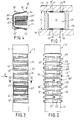
- contact strip Of the total designated 10 contact strip are in Figs. 1 and 5 respectively, only the outline of the insulating body 11 and the mutually opposite sides of the insulating body 11 over the outline protruding contact legs 12, 13 and 12 ', 13' shown. These contact legs are under outwardly directed spring tension, so that they create between two spaced at a distance 14 parallel printed circuit boards 15 and 16 force or pressure-locked to their associated tracks 17 and 18.
- the two printed circuit boards 15 and 16 which in the functional state, for example, have a clearance of only 3 mm or less, are held in parallel in a sandwich by means not shown.
- spacers 19 are schematically shown, the tightly flanking by virtue of their contact strip 10 as support body mapping ensure that the only pressure-locking clamped on their contact elements 12, 13, 12 ', 13' held between the plates held contact strip their intended location to the traces reliably.
- the contact legs denoted by 12 and 13 in FIG. 4 belong to a different contact element than those designated by 12 'and 13'. This is easily understood with reference to the illustration of FIG. 6.
- a contact element 20 has substantially the shape of the letter E.
- the two outer legs of the E are the contact legs 12 and 13. Between these two legs 12 and 13 is located
- This bearing section 21 is punched out of the same flat metal sheet of contact metal, in particular beryllium bronze, and merely bent, as are the contact legs 12 and 13.
- the bearing section 21 is connected to the material strip 23 via a short transition section 22 connected, from which the two legs 12 and 13 are punched out and deformed.
- the bearing portion 21 enters a plane which is laterally adjacent to the plane of the contact legs 12 and 13, by a distance x, which corresponds to the pitch or pole distance of the contact strip.
- the insulating body 11 is an injection molding of a highly dimensionally stable material having virtually no shrinkage.
- the insulating body has a number of thin webs 24, which are materially connected to one another via outline-smaller core portions 25. In the embodiment, two such core portions 25 are close together to form a slot 26.
- This slot 26 is thus an insulator slot into which a contact element 20 is inserted with its bearing portion 21 of one of the two possible sides and then firmly held therein.
- this bearing section 21 is located laterally next to the contact sections 12, 13 of the same contact element 20.
- the contact element with 20 'and its contact limb with 12' and 13 'arranged in the same plane as the bearing section 21 of the contact element 20 is logically distinguished ' designated.
- This contact element 20 ' is inserted with its in Fig. 4 not visible bearing portion from the other side into the adjacent insertion space.
- the contact strip 10 which is shown in Fig. 5, differs from the previously described contact strip 10 substantially only with respect to its in the drawing downwardly exiting contact legs 13 and 13 ', which formed as surface-parallel to the conductor 18 aligned SMT-Lötfishchen are.
- the upper circuit board 15 is still shown at a distance. In the operating state, however, it is the lower circuit board 16 so far approximated that create the contact legs 12 and 12 'of the relevant contact elements 20 and 20' under Eigenfedertik to the conductors 17.
- the tongue-shaped bearing portions 21 are each heldsverankernd in the Isolier Economicsschlitzen 26.
- the tongues 21 have edge edge formations 27 of approximately the type that can be seen in FIG. 6, which can engage in the plastic material of the insulating body 10.
- the contact strip 10 can be made in very small dimensions, for example, with grid spacing x of about 0.5 mm and for a PCB distance 14 of less than 3 mm.
Landscapes
- Coupling Device And Connection With Printed Circuit (AREA)
- Multi-Conductor Connections (AREA)
Claims (9)
- Connecteur de bords pour des cartes à circuits imprimés (15, 16) disposées en mode de construction en sandwich, avec un corps isolant (11) et une pluralité d'éléments de contact (20), disposés dans celui-ci selon un espacement tramé x, éléments de contact dont chacun présente un tronçon formant palier (21) pour sa fixation dans le corps isolant (11), ainsi que deux branches de contact (12, 13) à mettre en contact avec les pistes conductrices (17, 18) tournées l'une vers l'autre des cartes à circuits imprimés (15, 16), sachant que le tronçon de palier (21) est réalisé sous la forme de languette pouvant être introduite dans une fente de corps isolant (26), tournée dans la même direction que les branches de contact (12, 13) et disposée entre elles, caractérisé en ce que le tronçon de palier (21) est disposé latéralement à côté du plan défini par les branches de contact (12, 13), à la valeur de distance de trame x.
- Connecteur de bords selon la revendication 1, caractérisé en ce que l'élément de contact (20), observé en vue de côté, présente une forme sensiblement en E, dont les branches extérieures sont réalisées par les branches de contact (12, 13) et dont la branche centrale est réalisée par la languette (21).
- Connecteur de bords selon la revendication 1 ou 2, caractérisé par un agencement, en sens inverse d'un pôle à l'autre, des éléments de contact (20) dans le corps isolant (11).
- Connecteur de bords selon l'une des revendications 1 à 3, caractérisé en ce qu'au moins l'une des branches de contact (12, 13) des éléments de contact (20) est réalisée sous la forme de petites pattes à braser, en technique SMT (Surface Mounting Technique).
- Connecteur de bords selon l'une des revendications précédentes, caractérisé en ce que le connecteur de bords (10) est maintenu entre les cartes à circuits imprimés (15, 16), pratiquement purement par une liaison par pressage.
- Connecteur de bords selon la revendication 5, caractérisé en ce que le connecteur de bords (10) est orienté à l'aide de moyens d'orientation (13), à effet flanquant par rapport aux pistes conductrices (17, 18) des cartes à circuits imprimés (15, 16).
- Connecteur de bords selon la revendication 6, caractérisé en ce que les moyens d'orientation (13) servent en même temps de supports d'espacement pour les cartes à circuits imprimés (15, 16).
- Connecteur de bords selon la revendication 1 ou l'une des revendications suivantes, caractérisé en ce que le corps isolant (11) est réalisé sous la forme de pièces moulées par injection, monobloc.
- Connecteur de bords selon la revendication 1 ou l'une des revendications suivantes, caractérisé en ce que les éléments de contact (20) sont maintenus, par leurs tronçons de liaison (21), avec un effet d'auto-ancrage, dans les fentes de corps isolant (26).
Applications Claiming Priority (2)
| Application Number | Priority Date | Filing Date | Title |
|---|---|---|---|
| DE19617121A DE19617121C1 (de) | 1996-04-29 | 1996-04-29 | Kontaktleiste für Leiterplatten |
| DE19617121 | 1996-04-29 |
Publications (3)
| Publication Number | Publication Date |
|---|---|
| EP0805520A2 EP0805520A2 (fr) | 1997-11-05 |
| EP0805520A3 EP0805520A3 (fr) | 1999-01-13 |
| EP0805520B1 true EP0805520B1 (fr) | 2006-10-18 |
Family
ID=7792796
Family Applications (1)
| Application Number | Title | Priority Date | Filing Date |
|---|---|---|---|
| EP97102560A Expired - Lifetime EP0805520B1 (fr) | 1996-04-29 | 1997-02-18 | Connecteur de bords d'une carte à circuits imprimés |
Country Status (4)
| Country | Link |
|---|---|
| US (1) | US5951303A (fr) |
| EP (1) | EP0805520B1 (fr) |
| JP (1) | JP3742937B2 (fr) |
| DE (2) | DE19617121C1 (fr) |
Families Citing this family (11)
| Publication number | Priority date | Publication date | Assignee | Title |
|---|---|---|---|---|
| EP0903810A3 (fr) * | 1997-09-18 | 2000-03-29 | The Whitaker Corporation | Connecteur pour substrats adjacents portant un circuit |
| US6758702B2 (en) | 2000-02-24 | 2004-07-06 | Fci Americas Technology, Inc. | Electrical connector with compression contacts |
| US6488513B1 (en) | 2001-12-13 | 2002-12-03 | Intercon Systems, Inc. | Interposer assembly for soldered electrical connections |
| SG104969A1 (en) * | 2002-05-24 | 2004-07-30 | Fci Asia Technology Pte Ltd | An electrical connector |
| JP4427274B2 (ja) * | 2003-05-28 | 2010-03-03 | 佐鳥エス・テック株式会社 | 電動工具用スイッチ |
| US7455556B2 (en) * | 2003-06-11 | 2008-11-25 | Cinch Connectors, Inc. | Electrical contact |
| US6921270B2 (en) | 2003-06-11 | 2005-07-26 | Cinch Connectors, Inc. | Electrical connector |
| US7625216B2 (en) * | 2003-06-11 | 2009-12-01 | Cinch Connectors, Inc. | Electrical connector |
| US7435105B2 (en) * | 2004-03-29 | 2008-10-14 | Finisar Corporation | Electrical connector for use in an optical transceiver module |
| JP6821522B2 (ja) * | 2017-06-27 | 2021-01-27 | モレックス エルエルシー | ソケット |
| CN211605463U (zh) * | 2020-01-07 | 2020-09-29 | 番禺得意精密电子工业有限公司 | 电连接器 |
Family Cites Families (7)
| Publication number | Priority date | Publication date | Assignee | Title |
|---|---|---|---|---|
| US4699593A (en) * | 1986-01-14 | 1987-10-13 | Amp Incorporated | Connector having contact modules for a substrate such as an IC chip carrier |
| JP2535766Y2 (ja) * | 1990-12-17 | 1997-05-14 | 日本エー・エム・ピー株式会社 | 基板間相互接続装置 |
| US5125846A (en) * | 1991-07-25 | 1992-06-30 | Molex Incorporated | Input-output electrical connector |
| US5199884A (en) * | 1991-12-02 | 1993-04-06 | Amp Incorporated | Blind mating miniature connector |
| US5358411A (en) * | 1993-08-09 | 1994-10-25 | The Whitaker Corporation | Duplex plated epsilon compliant beam contact and interposer |
| KR950033507A (ko) * | 1994-02-08 | 1995-12-26 | 오가 노리오 | Ic 측정시험장치 및 이것을 사용한 ic 측정시험방법 |
| US5484295A (en) * | 1994-04-01 | 1996-01-16 | Teledyne Electronic Technologies | Low profile compression electrical connector |
-
1996
- 1996-04-29 DE DE19617121A patent/DE19617121C1/de not_active Expired - Fee Related
-
1997
- 1997-02-18 EP EP97102560A patent/EP0805520B1/fr not_active Expired - Lifetime
- 1997-02-18 DE DE59712749T patent/DE59712749D1/de not_active Expired - Fee Related
- 1997-04-10 JP JP12616297A patent/JP3742937B2/ja not_active Expired - Fee Related
- 1997-04-28 US US08/847,846 patent/US5951303A/en not_active Expired - Fee Related
Also Published As
| Publication number | Publication date |
|---|---|
| EP0805520A2 (fr) | 1997-11-05 |
| DE59712749D1 (de) | 2006-11-30 |
| JPH1050432A (ja) | 1998-02-20 |
| EP0805520A3 (fr) | 1999-01-13 |
| DE19617121C1 (de) | 1997-07-24 |
| JP3742937B2 (ja) | 2006-02-08 |
| US5951303A (en) | 1999-09-14 |
Similar Documents
| Publication | Publication Date | Title |
|---|---|---|
| DE69419406T2 (de) | Elektrischer verbinder zum verbinden von einer elektronischen speicherkarte | |
| DE68917080T2 (de) | Elektrischer Verbinder für elektronische Gedächtniskarten, Verfahren der Verwirklichung eines derartigen Verbinders und Lese-Schreibvorrichtung mit diesem Verbinder. | |
| DE69211742T2 (de) | Leiterplattensteckverbinder | |
| DE19634565C1 (de) | Kontaktträger | |
| DE1790342A1 (de) | Federkontaktteil | |
| DE10006530A1 (de) | Antennenfeder | |
| DE2234961C3 (de) | Verfahren zur Herstellung von Steckern für Schaltplatten | |
| DE2204924A1 (de) | Elektrische Verbinderanordnung | |
| DE2460704A1 (de) | Elektrischer kontakt | |
| DE4243076A1 (de) | Kotaktiereinrichtung für eine Chipkarte | |
| EP0805520B1 (fr) | Connecteur de bords d'une carte à circuits imprimés | |
| DE69609030T2 (de) | Elektrischer verbinder insbesondere für den anschluss einer elektronischen speicherkarte | |
| DE3590369C2 (fr) | ||
| DE1765584B1 (de) | Elektrische klemmanschlussverbindung zwischen einem isolierten draht oder zwei isolierten draehten und einem anschluss element | |
| DE2659645C2 (fr) | ||
| DE1915114A1 (de) | Aus Blech bestehendes elektrisches Kontaktelement | |
| EP0129068A1 (fr) | Relais électromagnétique miniaturisé et méthode de fabrication | |
| DE69119857T2 (de) | Verbindereinrichtung | |
| DE2345583C3 (de) | Steckerleiste | |
| DE69506750T2 (de) | Ebene Schaltungsplatte | |
| DE10061533B4 (de) | Selbsttragende Kontaktfeder, insbesondere für einen Smartcard-Connector | |
| DE3704240A1 (de) | Elektrische anordnung mit einer mehrzahl von gleitelementen | |
| DE2448349C2 (de) | Verbinderanordnung mit einem mit einer gedruckten Schaltungsplatte verbundenen Verbinder | |
| DE3855949T2 (de) | Gehäuse für integrierte Schaltungen | |
| DE29607758U1 (de) | Kontaktleiste für Leiterplatten |
Legal Events
| Date | Code | Title | Description |
|---|---|---|---|
| PUAI | Public reference made under article 153(3) epc to a published international application that has entered the european phase |
Free format text: ORIGINAL CODE: 0009012 |
|
| AK | Designated contracting states |
Kind code of ref document: A2 Designated state(s): DE FI FR GB IT NL SE |
|
| PUAL | Search report despatched |
Free format text: ORIGINAL CODE: 0009013 |
|
| AK | Designated contracting states |
Kind code of ref document: A3 Designated state(s): DE FI FR GB IT NL SE |
|
| 17P | Request for examination filed |
Effective date: 19981222 |
|
| RAP1 | Party data changed (applicant data changed or rights of an application transferred) |
Owner name: LUMBERG CONNECT GMBH & CO. KG |
|
| GRAP | Despatch of communication of intention to grant a patent |
Free format text: ORIGINAL CODE: EPIDOSNIGR1 |
|
| RIC1 | Information provided on ipc code assigned before grant |
Ipc: H01R 12/22 20060101ALI20060531BHEP Ipc: H01R 12/04 20060101AFI20060531BHEP |
|
| GRAS | Grant fee paid |
Free format text: ORIGINAL CODE: EPIDOSNIGR3 |
|
| GRAA | (expected) grant |
Free format text: ORIGINAL CODE: 0009210 |
|
| AK | Designated contracting states |
Kind code of ref document: B1 Designated state(s): DE FI FR GB IT NL SE |
|
| PG25 | Lapsed in a contracting state [announced via postgrant information from national office to epo] |
Ref country code: IT Free format text: LAPSE BECAUSE OF FAILURE TO SUBMIT A TRANSLATION OF THE DESCRIPTION OR TO PAY THE FEE WITHIN THE PRESCRIBED TIME-LIMIT;WARNING: LAPSES OF ITALIAN PATENTS WITH EFFECTIVE DATE BEFORE 2007 MAY HAVE OCCURRED AT ANY TIME BEFORE 2007. THE CORRECT EFFECTIVE DATE MAY BE DIFFERENT FROM THE ONE RECORDED. Effective date: 20061018 |
|
| REG | Reference to a national code |
Ref country code: GB Ref legal event code: FG4D Free format text: NOT ENGLISH |
|
| REF | Corresponds to: |
Ref document number: 59712749 Country of ref document: DE Date of ref document: 20061130 Kind code of ref document: P |
|
| GBT | Gb: translation of ep patent filed (gb section 77(6)(a)/1977) |
Effective date: 20061221 |
|
| REG | Reference to a national code |
Ref country code: SE Ref legal event code: TRGR |
|
| ET | Fr: translation filed | ||
| PLBE | No opposition filed within time limit |
Free format text: ORIGINAL CODE: 0009261 |
|
| STAA | Information on the status of an ep patent application or granted ep patent |
Free format text: STATUS: NO OPPOSITION FILED WITHIN TIME LIMIT |
|
| 26N | No opposition filed |
Effective date: 20070719 |
|
| PGFP | Annual fee paid to national office [announced via postgrant information from national office to epo] |
Ref country code: FI Payment date: 20080213 Year of fee payment: 12 Ref country code: SE Payment date: 20080213 Year of fee payment: 12 Ref country code: NL Payment date: 20080229 Year of fee payment: 12 Ref country code: IT Payment date: 20080228 Year of fee payment: 12 Ref country code: GB Payment date: 20080204 Year of fee payment: 12 |
|
| PGFP | Annual fee paid to national office [announced via postgrant information from national office to epo] |
Ref country code: FR Payment date: 20080226 Year of fee payment: 12 Ref country code: DE Payment date: 20080423 Year of fee payment: 12 |
|
| EUG | Se: european patent has lapsed | ||
| GBPC | Gb: european patent ceased through non-payment of renewal fee |
Effective date: 20090218 |
|
| PG25 | Lapsed in a contracting state [announced via postgrant information from national office to epo] |
Ref country code: FI Free format text: LAPSE BECAUSE OF NON-PAYMENT OF DUE FEES Effective date: 20090218 |
|
| NLV4 | Nl: lapsed or anulled due to non-payment of the annual fee |
Effective date: 20090901 |
|
| REG | Reference to a national code |
Ref country code: FR Ref legal event code: ST Effective date: 20091030 |
|
| PG25 | Lapsed in a contracting state [announced via postgrant information from national office to epo] |
Ref country code: NL Free format text: LAPSE BECAUSE OF NON-PAYMENT OF DUE FEES Effective date: 20090901 |
|
| PG25 | Lapsed in a contracting state [announced via postgrant information from national office to epo] |
Ref country code: DE Free format text: LAPSE BECAUSE OF NON-PAYMENT OF DUE FEES Effective date: 20090901 |
|
| PG25 | Lapsed in a contracting state [announced via postgrant information from national office to epo] |
Ref country code: GB Free format text: LAPSE BECAUSE OF NON-PAYMENT OF DUE FEES Effective date: 20090218 Ref country code: FR Free format text: LAPSE BECAUSE OF NON-PAYMENT OF DUE FEES Effective date: 20090302 |
|
| PG25 | Lapsed in a contracting state [announced via postgrant information from national office to epo] |
Ref country code: IT Free format text: LAPSE BECAUSE OF NON-PAYMENT OF DUE FEES Effective date: 20090218 |
|
| PG25 | Lapsed in a contracting state [announced via postgrant information from national office to epo] |
Ref country code: SE Free format text: LAPSE BECAUSE OF NON-PAYMENT OF DUE FEES Effective date: 20090219 |