EP0803972A1 - Zweiband-Oszillatorschaltung - Google Patents
Zweiband-Oszillatorschaltung Download PDFInfo
- Publication number
- EP0803972A1 EP0803972A1 EP97302805A EP97302805A EP0803972A1 EP 0803972 A1 EP0803972 A1 EP 0803972A1 EP 97302805 A EP97302805 A EP 97302805A EP 97302805 A EP97302805 A EP 97302805A EP 0803972 A1 EP0803972 A1 EP 0803972A1
- Authority
- EP
- European Patent Office
- Prior art keywords
- oscillator circuit
- dual band
- transistor
- frequency
- resonance
- Prior art date
- Legal status (The legal status is an assumption and is not a legal conclusion. Google has not performed a legal analysis and makes no representation as to the accuracy of the status listed.)
- Granted
Links
Images


Classifications
-
- H—ELECTRICITY
- H03—ELECTRONIC CIRCUITRY
- H03B—GENERATION OF OSCILLATIONS, DIRECTLY OR BY FREQUENCY-CHANGING, BY CIRCUITS EMPLOYING ACTIVE ELEMENTS WHICH OPERATE IN A NON-SWITCHING MANNER; GENERATION OF NOISE BY SUCH CIRCUITS
- H03B5/00—Generation of oscillations using amplifier with regenerative feedback from output to input
- H03B5/18—Generation of oscillations using amplifier with regenerative feedback from output to input with frequency-determining element comprising distributed inductance and capacitance
- H03B5/1841—Generation of oscillations using amplifier with regenerative feedback from output to input with frequency-determining element comprising distributed inductance and capacitance the frequency-determining element being a strip line resonator
- H03B5/1847—Generation of oscillations using amplifier with regenerative feedback from output to input with frequency-determining element comprising distributed inductance and capacitance the frequency-determining element being a strip line resonator the active element in the amplifier being a semiconductor device
Definitions
- the present invention relates to a small voltage-controlled oscillator (VCO) used in mobile communication systems such as mobile telephones and portable telephones and in satellite communication equipment.
- VCO voltage-controlled oscillator
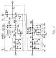
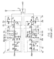
- Fig. 11 shows a prior art dual band oscillator circuit for generating signals of two different frequency bands.
- la denotes a first oscillator circuit portion
- 1b denotes a second oscillator circuit portion
- 2a denotes a first buffer amplifier portion
- 2b denotes a second buffer amplifier portion
- 3 denotes a single-pole double-throw switch
- 16a and 16b denote stage-to-stage coupling capacitors
- 22 denotes a high-frequency output terminal.
- the first oscillator circuit portion la utilizes a first frequency band
- the second oscillator circuit utilizes a second frequency band of the two frequency bands.
- An oscillation signal from the first oscillator circuit portion la is amplified in the first buffer amplifier portion 2a after passing the stage-to-stage coupling capacitor 16a.
- an oscillation signal from the second oscillator circuit portion 1b is amplified in the second buffer amplifier portion 2b after passing the stage-to-stage coupling capacitor 16b.
- the signals amplified in the buffer amplifier portions 2a and 2b are each input to the single-pole double-throw switch 3.
- a resonance circuit portion includes a combination of two inductors and a PIN diode switch.
- inductors operating as resonators are switched for switching resonance frequencies.
- a high-frequency oscillator circuit operating in a broad frequency band is implemented in this document.
- a dual band oscillator circuit comprises a first oscillator circuit for oscillating in a first frequency band, a second oscillator circuit for oscillating in a second frequency band, and a buffer amplifier circuit to which an output of the first oscillator circuit is input through a first stage-to-stage coupling element and an output of the second oscillator circuit is input through a second stage-to-stage coupling element, and input terminals for control voltages for controlling the first and second oscillator circuits to alternatively operate the first or second oscillator circuit.
- a single-pole double-throw switch for switching buffer amplifier outputs as used in a conventional circuit is unnecessary, and only one buffer amplifier circuit is necessary, rather than two.
- base voltages of oscillation transistors constituting the first and second oscillator circuits are respectively controlled by control voltages applied externally to provide switchable control of the oscillation transistor.
- a resonance circuit portion constituting the oscillator circuit such as a resonance circuit portion that changes a resonance frequency according to an externally applied voltage, may be provided in respective first and second oscillator circuits.
- the dual band oscillator circuit may comprise a dual band resonance circuit having both resonance frequencies of the first and second frequency bands, and the dual band resonance circuit is connected to the oscillation transistor of the first oscillator circuit via a first resonator-transistor coupling capacitor and is connected to the oscillation transistor of the second oscillator circuit via a second resonator-transistor coupling capacitor.
- the other end of the first resonator-transistor coupling capacitor connected to the oscillation transistor of the first oscillator circuit is connected to a position between the ground end and the open end of the strip line resonator of the dual band resonance circuit, the position being a node of a voltage standing wave caused by resonance of the second frequency band.
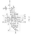
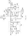
- Fig. 1 la denotes a first oscillator circuit portion, 1b denotes a second oscillator circuit portion, 2c denotes a buffer amplifier portion, 4a denotes a first resonance circuit portion, 4b denotes a second resonance circuit portion, 5a and 5b denote resonators, 6a and 6b denote resonator-varactor diode coupling capacitors, 7a and 7b denote varactor diodes, 8a, 8b, and 8c denote high-frequency chokes, 9a, 9b, and 9c denote high-frequency ground capacitors, 10a and 10b denote oscillation transistors, 11a and 11b denote collector-emitter capacitors, 12a and 12b denote collector-base capacitors, 13a and 13b denote emitter-ground capacitors, 14a and 14b denote base-ground capacitors, 15a and 15b denote resonator-transistor coupling capacitors, 16a and 16b denote stage-to-stage coupling capacitors, 17
- the first oscillator circuit portion la oscillates at a first frequency according to a voltage externally applied to the tuning voltage supply terminal 20a, and its oscillation output is provided to the buffer amplifier portion 2c through the stage-to-stage coupling capacitor 16a.
- the second oscillator circuit portion 1b oscillates at a second frequency according to a voltage externally applied to the tuning voltage supply terminal 20b, and its oscillation output is provided to the buffer amplifier portion 2c through the stage-to-stage coupling capacitor 16b.
- the first base bias control terminal 24a is provided to apply a control voltage externally to the base of the first oscillation transistor 10a through the base bias resistor 30a.
- the second base bias control terminal 24b is provided to apply a control voltage externally to the base of the second oscillation transistor 10b constituting the second oscillator circuit portion 1b through the base bias resistor 30b.
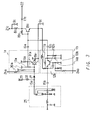
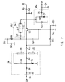
- Fig. 2 25 denotes a dual band resonance circuit portion
- 26 denotes a strip line resonator
- 6a and 6b denote resonator-varactor diode coupling capacitors
- 7c denotes a varactor diode
- 8c denotes a high-frequency choke
- 9c denotes a high-frequency ground capacitor
- 20c denotes a tuning voltage supply terminal
- other circuit elements are identical to those shown in Fig. 1, like elements being given like reference numbers.
- the strip line resonator 26 has one end grounded and the other end connected to the cathode terminal of the varactor diode 7c via the resonator-varactor diode coupling capacitor 6a. Also, the resonator-varactor diode coupling capacitor 6b is connected between a point on the strip line resonator 26b and the cathode terminal of the varactor diode 7c.
- the dual band resonance circuit 25 that resonates at two different frequencies is connected to the first oscillation transistor 10a via the resonator-transistor coupling capacitor 15a, and to the second oscillation transistor 10b via the resonator-transistor coupling capacitor 15b.
- the second oscillation transistor 10b When a predetermined voltage is applied to the second base bias control terminal 24b, and no voltage is applied to the first base bias control terminal 24a, the second oscillation transistor 10b is turned on, and the first oscillation transistor 10a is turned off. Since the capacitance values of each capacitor connected to the second oscillation transistor 10b are selected so that an optimal oscillation state can be obtained at the second frequency, an oscillator circuit is formed which utilizes the inductive reactance of the dual band resonance circuit portion 25 at a frequency band somewhat lower than the resonance frequency of the second frequency.
- the dual band oscillator circuit in this embodiment by using the dual band resonance circuit portion 25 that resonates at two frequencies, two conventional resonance circuit portions can be integrated into one. As a result, the size of the circuit can be reduced, resulting in a reduction in the size of the entire device.
- One end of the resonator-transistor coupling capacitor 15a is connected to the oscillation transistor 10a that oscillates at the first frequency, and the other end is connected to a point that is a node of the voltage standing wave resonating at the second frequency, in the strip line resonator 26.
- the adverse effects of connecting the oscillation transistor 10a via the resonator-transistor coupling capacitor 15a for example, a decrease in tuning voltage sensitivity with respect to the oscillation frequency of the second frequency band, are reduced.
- Table 2 The measured values of changes in oscillation frequency and changes in tuning voltage sensitivity in the second frequency band when changing the connection point of the resonator-transistor coupling capacitor 15a and the strip line resonator 26 are shown in Table 2.
- the emitter-ground capacitor 13a, the base-emitter capacitor 31a, the high-frequency ground capacitor 9a, and the resonator-transistor coupling capacitor 15a have respective capacitance values selected so that optimal oscillation occurs at a first frequency.
- 10b denotes the second oscillation transistor.
- the collector-emitter capacitor llb, the collector-base capacitor 12b, the emitter-ground capacitor 13b, the base-ground capacitor 14b, the resonator-transistor coupling capacitor 15b have respective capacitance values selected so that optimal oscillation occurs at a second frequency.
- the dual band resonance circuit portion 25 that resonates in two different frequencies is connected to the first oscillation transistor 10a that oscillates at the first frequency via the resonator-transistor coupling capacitor 15a and the switching diode 27, and is also connected to the second oscillation transistor 10b that oscillates at the second frequency via the resonator-transistor coupling capacitor 15b.
- the first oscillation transistor 10a and the switching diode 27 are turned on, and the second oscillation transistor 10b is turned off. Since the capacitance of each capacitor connected to the first oscillation transistor 10a is selected for optimal oscillation at the first frequency, an oscillator circuit is formed which utilizes the inductive reactance of the dual band resonance circuit portion 25 at a frequency somewhat lower than the resonance frequency of the first frequency.
- the second oscillation transistor 10b When a predetermined voltage is applied to the second base bias control terminal 24b, and no voltage is applied to the first base bias control terminal 24a, the second oscillation transistor 10b is turned on, and the first oscillation transistor 10a and the switching diode 27 are turned off. Since the capacitance of each capacitor connected to the second oscillation transistor 10b is selected for optimal oscillation at the second frequency, an oscillator circuit is formed which utilizes the inductive reactance of the dual band resonance circuit portion 25 at a frequency somewhat lower than the resonance frequency of the second frequency.
- the impedance of the circuit including the oscillation transistor 10a at the connection point of the resonance circuit portion 25 and the resonator-transistor coupling capacitor 15a can be made very large because the switching diode 27 is off.
- the capacitance value of the resonator-transistor coupling capacitor 15b can be selected so that the impedance is high at the first frequency, and that the impedance is low at the second frequency.
- the impedance of the circuit including the first oscillation transistor 10a at the connection point of the resonance circuit portion 25 and the resonator-transistor coupling capacitor 15a is very large because the switching diode 27 is off. Therefore, the adverse effects of connecting the first oscillation transistor 10a of the oscillator circuit on the non-operation side, for example, a decrease in tuning voltage sensitivity with respect to the oscillation frequency of the second frequency band, is reduced.
- the first oscillation transistor 10a that oscillates at the first frequency and the dual band resonance circuit portion 25 that resonates at two different frequencies are connected via the resonator-transistor coupling capacitor 15a and the switching diode 27.
- the adverse effects of the oscillation transistor 10a side are reduced.
- the resonator-transistor coupling capacitor 15b has a high impedance at the first frequency. Therefore, the adverse effect of the second oscillation transistor 10b on the oscillator circuit is similarly reduced.
- Fig. 4 is an embodiment of the present invention that implements the dual band resonance circuit portion 25 in Fig. 2 in another form.
- one end of a strip line 36b is grounded, and the other end is connected to the cathode terminal of a switching diode 27 as a switch means.
- the anode terminal of the switching diode 27 is connected to one end of a strip line 36a, the other end of which is connected to a first transistor circuit portion lc constituting a first oscillator circuit via a resonator-transistor coupling capacitor 15a.
- a point on the strip line 36b is connected to a second transistor circuit portion 1d constituting a second oscillator circuit via a resonator-transistor coupling capacitor 15b.
- the anode terminal of the switching diode 27 is connected to a band switching terminal 35 via a switching diode bias choke coil 28, and the band switching terminal 35 is grounded by a bypass capacitor 34.
- the sum L1 of the lengths of the strip lines 36a and 36b is set to a 1/4 of the wavelength of a required first resonance frequency.
- the length L2 of the strip line 36b is a 1/4 of the wavelength of a required second resonance frequency.
- the first resonance frequency is lower than the second resonance frequency.
- the resonance frequencies are switched depending on whether a positive voltage is applied to the band switching terminal 35.
- the switching diode 27 When a positive voltage is applied, the switching diode 27 is forward biased to be conductive. Therefore, the strip lines 36a and 36b operate co-operatively as an end grounded resonator. Then, the resonance frequency of the resonance circuit is determined by the sum of the lengths of the two lines.
- the coupling portion between the first transistor circuit portion 1c and the buffer amplifier portion 2c is constituted by a parallel resonance circuit including the stage-to-stage coupling capacitor 16a and the stage-to-stage coil 32. Also, the direct-current blocking capacitor 33 is added for cutting a direct-current bias.
- the capacitance value of the stage-to-stage coupling capacitor 16a and the inductance value of the stage-to-stage coil 32 are set so that the parallel resonance frequency is close to the second oscillation frequency of the second transistor circuit portion 1d constituting the second oscillator circuit.
- the impedance of the first transistor circuit lc at the coupling point of the stage-to-stage coupling capacitors 16a and 16b and the buffer amplifier portion 2c can be made to be very large.
- the capacitance value of the stage-to-stage coupling capacitor 16b may be selected to have a high impedance at the first oscillation frequency produced by the first transistor circuit portion 1c, and a low impedance at the second oscillation frequency produced by the second transistor circuit portion 1d.
- the oscillation signal at the second frequency is amplified in the buffer amplifier portion 2c to be output from the high-frequency output terminal 22, and is minimally affected by the connection of the first transistor circuit portion 1c.
- the coupling portion between the first transistor circuit portion 1c and the buffer amplifier portion 2c is constituted by the parallel resonance circuit of the stage-to-stage coupling capacitor 16a and the stage-to-stage coil 32. Therefore, when oscillating at the second frequency, with the second transistor circuit portion 1d, the effect of the first transistor circuit portion 1c can be eliminated to avoid a decrease in oscillation output.
- stage-to-stage coupling capacitor 16a is removed to set the series resonance frequency by the stage-to-stage coil 32 and the direct-current blocking capacitor 33 to be between the oscillation frequencies of the first oscillator circuit (i.e., the transistor circuit portion 1c) and the second oscillator circuit (i.e., the transistor circuit portion 1d).
- a resonance circuit block 55 functions as an inductive impedance circuit and has a high Q value as a resonance circuit.
- a tuning voltage supply terminal 20c is connected to the cathode side of a varactor diode 7c and to a resonator-varactor coupling capacitor 6c by a high-frequency choke 8c having an appropriate inductance value.
- the anode side of the varactor diode 7c is grounded.
- a strip line resonator 26 connected to the other end of the resonator-varactor coupling capacitor 6c has a required inductance component at a desired frequency band and may be formed on a dielectric substrate.
- a base-ground capacitor 14c is connected between the base of the transistor 10c and the ground to operate the transistor 10c as a grounded base type high-frequency oscillator circuit.
- the output is obtained from an output terminal 22 through a stage-to-stage coupling capacitor 16c connected to the emitter of the transistor 10c.
- Feedback blocks 38b and 38c having a similar circuit configuration are connected between the emitter of the transistor 10c and the ground, and between the collector and base of the transistor 10c, respectively.
- the value of each element constituting the respective feedback blocks is selected in a manner similar to that of 38a.
- the resonance circuit block 55 may resonate at two different frequencies depending on whether a positive voltage is applied to the band switching terminal 35.
- the resonance circuit block 55 has an inductive impedance at the first frequency. Since each of the feedback circuit blocks 38a, 38b and 38c has an impedance adjusted to satisfy the oscillation condition at the first frequency and optimize the C/N ratio, the oscillation condition at the first oscillation frequency is satisfied, and an output at the first oscillation frequency is obtained from the high-frequency output terminal 22.
- the resonance circuit block 55 When producing an oscillation output at the second frequency, no positive voltage is applied to the band switching terminal 35, thus setting the switching diode 27 in an "off" state.
- the resonance circuit block 55 has an inductive impedance in the second frequency band. Since each of the feedback circuit blocks 38a, 38b and 38c has an impedance adjusted to satisfy the oscillation condition at the second frequency band and optimize the C/N ratio, the oscillation condition at the second oscillation frequency is satisfied, and an output at the second oscillation frequency is obtained from the high-frequency output terminal 22.
- oscillation in two different frequency bands can be implemented without any degradation in C/N ratio characteristics.
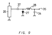
- FIG. 9 Another example of a configuration of a resonator and a semiconductor switch element in resonance circuit block 55 in this embodiment is shown in Fig. 9.
- a strip line resonator 26 is grounded, the anode of a switching diode 27 is connected to one point on the strip line resonator 26 via a capacitor for DC isolation, and the cathode of the diode 27 is grounded.
- the switching diode 27 is turned on/off, depending on whether a positive voltage is applied to a band switching terminal 35 or not, and the line length to the short-circuit end, a tip end, of the strip line resonator 26 is changed.
- the resonance frequency can be changed, and the resonance circuit block 55 can obtain resonance in two different frequency bands.
- a resonator-transistor coupling capacitor 15c is connected between the connection point of strip line the resonators 48 and 49 and the collector of an oscillation transistor 10c.
- a feedback circuit block 38d is connected between the collector and emitter of the oscillation transistor 10c and is constituted by a circuit in which a capacitor 52 is connected in series with the parallel circuit of a capacitor 53 and a strip line 54 formed on a dielectric substrate.
- the characteristics of two capacitors 52 and 53, and the strip line 54 are selected to satisfy the oscillation condition at two desired frequencies and obtain a desired capacitive impedance for high C/N ratio characteristics in the same way as in the feedback circuit block 38a in Fig. 6.
- a feedback circuit block 38e is connected between the emitter of the oscillation transistor 10c and ground, and capacitors 50 and 51 are connected to the emitter of the oscillation transistor 10c.
- the anode of a switching diode 27 is connected to an oscillation frequency band switching terminal 35 via a switching diode bias choke 28, and the cathode of the switching diode 27 is grounded.
- the capacitive impedance between the emitter of the oscillation transistor 10c and the ground is switched by turning the switching diode 27 on and off by a control voltage signal applied to the band switching control terminal 35.
- the capacitances of the capacitors 50, 51 are selected so that the oscillation condition in two desired frequency bands and high C/N ratio characteristics can be satisfied.
- the dual band resonance circuit 25 has no switch such as a semiconductor switch element. However, it has a resonance frequency somewhat higher than the desired two oscillation frequencies and functions as a desired inductive impedance circuit in two frequency bands.
- the feedback circuit block 38d has a desired capacitive impedance in two oscillation frequency bands.
- the feedback circuit block 38e similarly has a desired capacitive impedance in two oscillation frequency bands depending on a control voltage from the band switching terminal 35.
- oscillation in two desired frequency bands can be implemented with a high C/N ratio value.
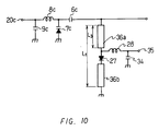
- a similar effect is obtained if the resonator portion of the dual band resonance circuit portion 25 is configured as shown in Fig. 10 in this embodiment.
- one end of a strip line 36b is grounded, and the other end is connected to the cathode of a switching diode 27, the anode of which is connected to one end of a strip line 36a, the other end of which is connected to the cathode of a varactor diode 7c via a resonator-varactor coupling capacitor 6c.
- the anode of the varactor diode 7c is grounded.
- a tuning voltage from a tuning voltage supply terminal 20c is applied to the varactor diode through a high-frequency choke 8c.
- the anode of the switching diode 27 is connected to the band switching terminal 35 via a switching diode bias choke coil 28.
- Adjustment of the oscillation frequency is performed by adjusting the length L3 of the strip line 36a when the switching diode 27 is off, and by adjusting-the sum L1 of the lengths of the strip lines 36a and 36b when the switching diode 27 is on.
- the oscillator circuit can be operated at any two frequencies.
Landscapes
- Inductance-Capacitance Distribution Constants And Capacitance-Resistance Oscillators (AREA)
Applications Claiming Priority (9)
| Application Number | Priority Date | Filing Date | Title |
|---|---|---|---|
| JP105798/96 | 1996-04-25 | ||
| JP10579896 | 1996-04-25 | ||
| JP8105798A JPH09294018A (ja) | 1996-04-25 | 1996-04-25 | 高周波二帯域発振回路 |
| JP119098/96 | 1996-05-14 | ||
| JP11909896 | 1996-05-14 | ||
| JP8119098A JPH09307354A (ja) | 1996-05-14 | 1996-05-14 | 共振器とこれを用いた電圧制御発振器 |
| JP8153565A JPH104315A (ja) | 1996-06-14 | 1996-06-14 | 高周波発振回路 |
| JP15356596 | 1996-06-14 | ||
| JP153565/96 | 1996-06-14 |
Publications (2)
| Publication Number | Publication Date |
|---|---|
| EP0803972A1 true EP0803972A1 (de) | 1997-10-29 |
| EP0803972B1 EP0803972B1 (de) | 2002-09-25 |
Family
ID=27310580
Family Applications (1)
| Application Number | Title | Priority Date | Filing Date |
|---|---|---|---|
| EP97302805A Expired - Lifetime EP0803972B1 (de) | 1996-04-25 | 1997-04-24 | Zweiband-Oszillatorschaltung |
Country Status (4)
| Country | Link |
|---|---|
| US (1) | US5852384A (de) |
| EP (1) | EP0803972B1 (de) |
| CN (1) | CN1083171C (de) |
| DE (1) | DE69715717T2 (de) |
Cited By (5)
| Publication number | Priority date | Publication date | Assignee | Title |
|---|---|---|---|---|
| WO2000019612A1 (en) * | 1998-09-30 | 2000-04-06 | Conexant Systems, Inc. | Dual frequency synthesis system |
| EP1154559A3 (de) * | 2000-03-30 | 2002-06-12 | Alps Electric Co., Ltd. | Oszillator |
| KR100372057B1 (ko) * | 1999-10-14 | 2003-02-11 | 알프스 덴키 가부시키가이샤 | 2밴드 발진기 |
| EP1271788A3 (de) * | 2001-06-29 | 2004-10-20 | Motorola, Inc. | Schaltungen zur Funkkommunikation |
| WO2013083735A3 (en) * | 2011-12-06 | 2013-08-15 | St-Ericsson Sa | Oscillator having dual topology |
Families Citing this family (35)
| Publication number | Priority date | Publication date | Assignee | Title |
|---|---|---|---|---|
| US6072371A (en) * | 1997-06-16 | 2000-06-06 | Trw Inc. | Quenchable VCO for switched band synthesizer applications |
| AU3784499A (en) * | 1998-05-05 | 1999-11-23 | Vari-L Company, Inc. | Passive switched oscillator output circuit |
| US6167245A (en) * | 1998-05-29 | 2000-12-26 | Silicon Laboratories, Inc. | Method and apparatus for operating a PLL with a phase detector/sample hold circuit for synthesizing high-frequency signals for wireless communications |
| US7221921B2 (en) | 1998-05-29 | 2007-05-22 | Silicon Laboratories | Partitioning of radio-frequency apparatus |
| US7035607B2 (en) | 1998-05-29 | 2006-04-25 | Silicon Laboratories Inc. | Systems and methods for providing an adjustable reference signal to RF circuitry |
| US6150891A (en) * | 1998-05-29 | 2000-11-21 | Silicon Laboratories, Inc. | PLL synthesizer having phase shifted control signals |
| US6993314B2 (en) | 1998-05-29 | 2006-01-31 | Silicon Laboratories Inc. | Apparatus for generating multiple radio frequencies in communication circuitry and associated methods |
| US6233441B1 (en) | 1998-05-29 | 2001-05-15 | Silicon Laboratories, Inc. | Method and apparatus for generating a discretely variable capacitance for synthesizing high-frequency signals for wireless communications |
| US6147567A (en) * | 1998-05-29 | 2000-11-14 | Silicon Laboratories Inc. | Method and apparatus for providing analog and digitally controlled capacitances for synthesizing high-frequency signals for wireless communications |
| US6308055B1 (en) | 1998-05-29 | 2001-10-23 | Silicon Laboratories, Inc. | Method and apparatus for operating a PLL for synthesizing high-frequency signals for wireless communications |
| US7242912B2 (en) | 1998-05-29 | 2007-07-10 | Silicon Laboratories Inc. | Partitioning of radio-frequency apparatus |
| US6327463B1 (en) | 1998-05-29 | 2001-12-04 | Silicon Laboratories, Inc. | Method and apparatus for generating a variable capacitance for synthesizing high-frequency signals for wireless communications |
| US6304146B1 (en) | 1998-05-29 | 2001-10-16 | Silicon Laboratories, Inc. | Method and apparatus for synthesizing dual band high-frequency signals for wireless communications |
| US7092675B2 (en) | 1998-05-29 | 2006-08-15 | Silicon Laboratories | Apparatus and methods for generating radio frequencies in communication circuitry using multiple control signals |
| US6311050B1 (en) | 1998-05-29 | 2001-10-30 | Silicon Laboratories, Inc. | Single integrated circuit phase locked loop for synthesizing high-frequency signals for wireless communications and method for operating same |
| US6137372A (en) | 1998-05-29 | 2000-10-24 | Silicon Laboratories Inc. | Method and apparatus for providing coarse and fine tuning control for synthesizing high-frequency signals for wireless communications |
| US6226506B1 (en) | 1998-05-29 | 2001-05-01 | Silicon Laboratories, Inc. | Method and apparatus for eliminating floating voltage nodes within a discreetly variable capacitance used for synthesizing high-frequency signals for wireless communications |
| US6574288B1 (en) | 1998-05-29 | 2003-06-03 | Silicon Laboratories Inc. | Method and apparatus for adjusting a digital control word to tune synthesized high-frequency signals for wireless communications |
| JP2001060826A (ja) * | 1999-08-19 | 2001-03-06 | Alps Electric Co Ltd | 2バンド発振装置 |
| JP2001237640A (ja) * | 2000-02-21 | 2001-08-31 | Murata Mfg Co Ltd | 電圧制御発振器および通信装置 |
| US6504443B1 (en) * | 2000-05-17 | 2003-01-07 | Nec America, Inc., | Common anode varactor tuned LC circuit |
| US6903617B2 (en) | 2000-05-25 | 2005-06-07 | Silicon Laboratories Inc. | Method and apparatus for synthesizing high-frequency signals for wireless communications |
| US6323735B1 (en) | 2000-05-25 | 2001-11-27 | Silicon Laboratories, Inc. | Method and apparatus for synthesizing high-frequency signals utilizing on-package oscillator circuit inductors |
| JP2001345638A (ja) * | 2000-06-01 | 2001-12-14 | Alps Electric Co Ltd | 3バンド切替型発振器 |
| JP2002043843A (ja) * | 2000-07-27 | 2002-02-08 | Murata Mfg Co Ltd | 電圧制御発振器及びそれを用いた通信機 |
| JP2002261543A (ja) | 2001-03-06 | 2002-09-13 | Alps Electric Co Ltd | 2バンド発振器 |
| US6930561B2 (en) * | 2002-09-24 | 2005-08-16 | Honeywell International, Inc. | Multi-band voltage controlled oscillator |
| JP2006238034A (ja) * | 2005-02-24 | 2006-09-07 | Alps Electric Co Ltd | 発振回路 |
| JP5870836B2 (ja) * | 2012-05-08 | 2016-03-01 | ソニー株式会社 | 受信装置および半導体集積回路 |
| CN103633941B (zh) * | 2013-11-27 | 2016-08-17 | 中国科学院微电子研究所 | 一种产生双频信号的毫米波振荡器 |
| US10926007B2 (en) * | 2015-07-13 | 2021-02-23 | Conmed Corporation | Surgical suction device that uses positive pressure gas |
| CN110247171B (zh) * | 2019-07-04 | 2024-05-17 | 深圳迈睿智能科技有限公司 | 天线和其工作电路及制造方法 |
| US11025231B1 (en) | 2020-04-16 | 2021-06-01 | Silicon Laboratories Inc. | Providing a programmable inductor to enable wide tuning range |
| TWI744069B (zh) * | 2020-11-03 | 2021-10-21 | 立積電子股份有限公司 | 射頻放大裝置 |
| US11646705B2 (en) | 2021-06-30 | 2023-05-09 | Silicon Laboratories Inc. | Dual-mode power amplifier for wireless communication |
Citations (5)
| Publication number | Priority date | Publication date | Assignee | Title |
|---|---|---|---|---|
| DE2607530A1 (de) * | 1976-02-25 | 1977-09-01 | Bosch Gmbh Robert | Funksende- und/oder -empfangsgeraet mit einer oszillatoren-einrichtung |
| JPS626504A (ja) * | 1985-07-03 | 1987-01-13 | Hitachi Ltd | 電圧制御発振器 |
| US5263182A (en) * | 1988-05-18 | 1993-11-16 | Samsung Electronics Co., Ltd. | Low-noise block converter for a satellite broadcasting system |
| US5420646A (en) * | 1991-12-30 | 1995-05-30 | Zenith Electronics Corp. | Bandswitched tuning system having a plurality of local oscillators for a digital television receiver |
| EP0696843A1 (de) * | 1994-08-11 | 1996-02-14 | Matsushita Electric Industrial Co., Ltd. | Oszillator sowie den Oszillator verwendende Frequenzsynthesizer und Kommunikationsgeräte |
Family Cites Families (5)
| Publication number | Priority date | Publication date | Assignee | Title |
|---|---|---|---|---|
| JPS4955209A (de) * | 1972-09-29 | 1974-05-29 | ||
| US4353038A (en) * | 1981-03-31 | 1982-10-05 | Motorola, Inc. | Wideband, synthesizer switched element voltage controlled oscillator |
| JPH0349458Y2 (de) * | 1985-03-14 | 1991-10-22 | ||
| US5200713A (en) * | 1990-10-04 | 1993-04-06 | Wiltron Company | Multiple magnetically tuned oscillator |
| JPH05259737A (ja) * | 1992-03-16 | 1993-10-08 | Tokimec Inc | 誘電体発振器 |
-
1997
- 1997-04-18 US US08/844,039 patent/US5852384A/en not_active Expired - Lifetime
- 1997-04-24 DE DE69715717T patent/DE69715717T2/de not_active Expired - Fee Related
- 1997-04-24 EP EP97302805A patent/EP0803972B1/de not_active Expired - Lifetime
- 1997-04-25 CN CN97111280A patent/CN1083171C/zh not_active Expired - Fee Related
Patent Citations (5)
| Publication number | Priority date | Publication date | Assignee | Title |
|---|---|---|---|---|
| DE2607530A1 (de) * | 1976-02-25 | 1977-09-01 | Bosch Gmbh Robert | Funksende- und/oder -empfangsgeraet mit einer oszillatoren-einrichtung |
| JPS626504A (ja) * | 1985-07-03 | 1987-01-13 | Hitachi Ltd | 電圧制御発振器 |
| US5263182A (en) * | 1988-05-18 | 1993-11-16 | Samsung Electronics Co., Ltd. | Low-noise block converter for a satellite broadcasting system |
| US5420646A (en) * | 1991-12-30 | 1995-05-30 | Zenith Electronics Corp. | Bandswitched tuning system having a plurality of local oscillators for a digital television receiver |
| EP0696843A1 (de) * | 1994-08-11 | 1996-02-14 | Matsushita Electric Industrial Co., Ltd. | Oszillator sowie den Oszillator verwendende Frequenzsynthesizer und Kommunikationsgeräte |
Non-Patent Citations (1)
| Title |
|---|
| PATENT ABSTRACTS OF JAPAN vol. 011, no. 171 (E - 512) 2 June 1987 (1987-06-02) * |
Cited By (6)
| Publication number | Priority date | Publication date | Assignee | Title |
|---|---|---|---|---|
| WO2000019612A1 (en) * | 1998-09-30 | 2000-04-06 | Conexant Systems, Inc. | Dual frequency synthesis system |
| KR100372057B1 (ko) * | 1999-10-14 | 2003-02-11 | 알프스 덴키 가부시키가이샤 | 2밴드 발진기 |
| EP1154559A3 (de) * | 2000-03-30 | 2002-06-12 | Alps Electric Co., Ltd. | Oszillator |
| EP1271788A3 (de) * | 2001-06-29 | 2004-10-20 | Motorola, Inc. | Schaltungen zur Funkkommunikation |
| WO2013083735A3 (en) * | 2011-12-06 | 2013-08-15 | St-Ericsson Sa | Oscillator having dual topology |
| US9252705B2 (en) | 2011-12-06 | 2016-02-02 | St-Ericsson Sa | Oscillator having dual topology |
Also Published As
| Publication number | Publication date |
|---|---|
| CN1167363A (zh) | 1997-12-10 |
| DE69715717T2 (de) | 2003-05-22 |
| US5852384A (en) | 1998-12-22 |
| CN1083171C (zh) | 2002-04-17 |
| DE69715717D1 (de) | 2002-10-31 |
| EP0803972B1 (de) | 2002-09-25 |
Similar Documents
| Publication | Publication Date | Title |
|---|---|---|
| US5852384A (en) | Dual band oscillator circuit using strip line resonators | |
| EP1023769B1 (de) | Spannungsgesteuerter doppelbandoszillator | |
| US5856763A (en) | Dual frequency voltage controlled oscillator | |
| US4621241A (en) | Wide range electronic oscillator | |
| KR940005381B1 (ko) | 다대역 튜너용 튜닝 회로 | |
| EP0893878B1 (de) | Hochfrequenz-Oszillatorschaltung | |
| US5748051A (en) | Low phase noise UHF and microwave oscillator | |
| US5982243A (en) | Oscillator selectively operable with a parallel tuned or a series tuned resonant circuit | |
| JPH07107961B2 (ja) | テレビジョン受像機用局部発振器 | |
| US7227421B2 (en) | Crystal oscillator circuit | |
| JP2553949B2 (ja) | 発振器 | |
| JPH09294018A (ja) | 高周波二帯域発振回路 | |
| EP1079512B1 (de) | Zweibandoszillatorgerät | |
| US5621362A (en) | Cascode oscillator having optimum phase noise and bandwidth performance | |
| JPH0746038A (ja) | 電圧制御周波数発振器 | |
| US6456169B2 (en) | Voltage-controlled oscillator and electronic device using same | |
| US20020050866A1 (en) | Voltage controlled oscillator and communication device using the same | |
| KR100447743B1 (ko) | 복수의 공진기를 포함하는 전압제어 발진 장치 | |
| US5512862A (en) | Oscillator with improved sideband noise | |
| KR100354241B1 (ko) | 전압제어발진기 | |
| KR100285307B1 (ko) | 동축공진기를이용한lc발진회로를구비하는전압제어발진기 | |
| US20050110588A1 (en) | Oscillator | |
| EP1081846B1 (de) | Spannungsgesteuerter Oszillator | |
| KR20020083709A (ko) | 다중대역 전압제어 발진기 회로 | |
| CN100511969C (zh) | 双频带电压控制振荡电路 |
Legal Events
| Date | Code | Title | Description |
|---|---|---|---|
| PUAI | Public reference made under article 153(3) epc to a published international application that has entered the european phase |
Free format text: ORIGINAL CODE: 0009012 |
|
| AK | Designated contracting states |
Kind code of ref document: A1 Designated state(s): DE FR GB |
|
| 17P | Request for examination filed |
Effective date: 19980309 |
|
| 17Q | First examination report despatched |
Effective date: 20001107 |
|
| GRAG | Despatch of communication of intention to grant |
Free format text: ORIGINAL CODE: EPIDOS AGRA |
|
| GRAG | Despatch of communication of intention to grant |
Free format text: ORIGINAL CODE: EPIDOS AGRA |
|
| GRAH | Despatch of communication of intention to grant a patent |
Free format text: ORIGINAL CODE: EPIDOS IGRA |
|
| GRAH | Despatch of communication of intention to grant a patent |
Free format text: ORIGINAL CODE: EPIDOS IGRA |
|
| GRAA | (expected) grant |
Free format text: ORIGINAL CODE: 0009210 |
|
| AK | Designated contracting states |
Kind code of ref document: B1 Designated state(s): DE FR GB |
|
| REG | Reference to a national code |
Ref country code: GB Ref legal event code: FG4D |
|
| REF | Corresponds to: |
Ref document number: 69715717 Country of ref document: DE Date of ref document: 20021031 |
|
| ET | Fr: translation filed | ||
| PLBE | No opposition filed within time limit |
Free format text: ORIGINAL CODE: 0009261 |
|
| STAA | Information on the status of an ep patent application or granted ep patent |
Free format text: STATUS: NO OPPOSITION FILED WITHIN TIME LIMIT |
|
| 26N | No opposition filed |
Effective date: 20030626 |
|
| PGFP | Annual fee paid to national office [announced via postgrant information from national office to epo] |
Ref country code: FR Payment date: 20090417 Year of fee payment: 13 Ref country code: DE Payment date: 20090420 Year of fee payment: 13 |
|
| PGFP | Annual fee paid to national office [announced via postgrant information from national office to epo] |
Ref country code: GB Payment date: 20090422 Year of fee payment: 13 |
|
| GBPC | Gb: european patent ceased through non-payment of renewal fee |
Effective date: 20100424 |
|
| REG | Reference to a national code |
Ref country code: FR Ref legal event code: ST Effective date: 20101230 |
|
| PG25 | Lapsed in a contracting state [announced via postgrant information from national office to epo] |
Ref country code: DE Free format text: LAPSE BECAUSE OF NON-PAYMENT OF DUE FEES Effective date: 20101103 |
|
| PG25 | Lapsed in a contracting state [announced via postgrant information from national office to epo] |
Ref country code: GB Free format text: LAPSE BECAUSE OF NON-PAYMENT OF DUE FEES Effective date: 20100424 |
|
| PG25 | Lapsed in a contracting state [announced via postgrant information from national office to epo] |
Ref country code: FR Free format text: LAPSE BECAUSE OF NON-PAYMENT OF DUE FEES Effective date: 20100430 |