EP0803908A2 - Halbleiteranordnung mit einer Schutzvorrichtung - Google Patents
Halbleiteranordnung mit einer Schutzvorrichtung Download PDFInfo
- Publication number
- EP0803908A2 EP0803908A2 EP97106484A EP97106484A EP0803908A2 EP 0803908 A2 EP0803908 A2 EP 0803908A2 EP 97106484 A EP97106484 A EP 97106484A EP 97106484 A EP97106484 A EP 97106484A EP 0803908 A2 EP0803908 A2 EP 0803908A2
- Authority
- EP
- European Patent Office
- Prior art keywords
- type
- transistor
- gate
- protective
- pads
- Prior art date
- Legal status (The legal status is an assumption and is not a legal conclusion. Google has not performed a legal analysis and makes no representation as to the accuracy of the status listed.)
- Withdrawn
Links
Images


Classifications
-
- H—ELECTRICITY
- H10—SEMICONDUCTOR DEVICES; ELECTRIC SOLID-STATE DEVICES NOT OTHERWISE PROVIDED FOR
- H10D—INORGANIC ELECTRIC SEMICONDUCTOR DEVICES
- H10D84/00—Integrated devices formed in or on semiconductor substrates that comprise only semiconducting layers, e.g. on Si wafers or on GaAs-on-Si wafers
- H10D84/80—Integrated devices formed in or on semiconductor substrates that comprise only semiconducting layers, e.g. on Si wafers or on GaAs-on-Si wafers characterised by the integration of at least one component covered by groups H10D12/00 or H10D30/00, e.g. integration of IGFETs
- H10D84/82—Integrated devices formed in or on semiconductor substrates that comprise only semiconducting layers, e.g. on Si wafers or on GaAs-on-Si wafers characterised by the integration of at least one component covered by groups H10D12/00 or H10D30/00, e.g. integration of IGFETs of only field-effect components
-
- H—ELECTRICITY
- H10—SEMICONDUCTOR DEVICES; ELECTRIC SOLID-STATE DEVICES NOT OTHERWISE PROVIDED FOR
- H10D—INORGANIC ELECTRIC SEMICONDUCTOR DEVICES
- H10D89/00—Aspects of integrated devices not covered by groups H10D84/00 - H10D88/00
- H10D89/60—Integrated devices comprising arrangements for electrical or thermal protection, e.g. protection circuits against electrostatic discharge [ESD]
- H10D89/601—Integrated devices comprising arrangements for electrical or thermal protection, e.g. protection circuits against electrostatic discharge [ESD] for devices having insulated gate electrodes, e.g. for IGFETs or IGBTs
- H10D89/811—Integrated devices comprising arrangements for electrical or thermal protection, e.g. protection circuits against electrostatic discharge [ESD] for devices having insulated gate electrodes, e.g. for IGFETs or IGBTs using FETs as protective elements
-
- H—ELECTRICITY
- H02—GENERATION; CONVERSION OR DISTRIBUTION OF ELECTRIC POWER
- H02H—EMERGENCY PROTECTIVE CIRCUIT ARRANGEMENTS
- H02H9/00—Emergency protective circuit arrangements for limiting excess current or voltage without disconnection
- H02H9/04—Emergency protective circuit arrangements for limiting excess current or voltage without disconnection responsive to excess voltage
- H02H9/045—Emergency protective circuit arrangements for limiting excess current or voltage without disconnection responsive to excess voltage adapted to a particular application and not provided for elsewhere
- H02H9/046—Emergency protective circuit arrangements for limiting excess current or voltage without disconnection responsive to excess voltage adapted to a particular application and not provided for elsewhere responsive to excess voltage appearing at terminals of integrated circuits
Definitions
- the present invention relates to a semiconductor integrated circuit, and more particularly to a transfer gate which uses an insulated gate electric field effect transistor (referred to as a MOS transistor, hereinafter).
- MOS transistor insulated gate electric field effect transistor
- Fig. 1 is a circuit diagram showing one constitutional example of a conventional semiconductor device.
- this conventional semiconductor device is composed of an analog switch 130, which is for transmitting an analog signal from an input pad to an output pad, and a protective circuit 20, which is for protecting the analog switch 130.
- a signal input from an analog signal 9 is transmitted through the analog switch 130 and the protective circuit 20 to a bonding pad 1
- a signal input from the bonding pad 1 is transmitted through the protective circuit 20 and the analog switch 130 to the analog signal 9, and so on.
- the analog switch 130 there are provided side by side a P type transfer gate 4 and an N type transfer gate 5, to whose gate terminals reverse phase control signals 10 are input by inverters 6a and 6b respectively.
- a P type protective transistor 2 with its source and gate terminals connected to a power supply potential 7 and its drain terminal connected to the bonding pad 1, and an N type protective transistor 3, with its source and gate terminals connected to a ground potential and its drain terminal connected to the bonding pad 1.
- Fig. 2 is a view showing a layout example of the analog switch 130 shown in Fig. 1.
- Fig. 3(a) is a section view taken along the line C-C' of the analog switch 130 shown in Fig. 2
- Fig. 3(b) is a section view taken along the line D-D' of the analog switch 130 shown in Fig. 2.
- the bonding pad 1 is connected through a second layer metallic wiring 101-1 and first layer metallic wirings 102-1 and 102-4 to the N type diffusion layers 104-1 and 104-3 of the N type transfer gate 4 and to the P type diffusion layers 103-2 and 103-4 of the P type transfer gate 5. Thereby, the bonding pad 1 and the analog switch 130 are interconnected.
- an N type diffusion layer 104-2 in the internal side of the N type transfer gate 5 and a P type diffusion layer 103-3 in the internal side of the P type transfer gate 4 are connected through a first layer metallic wiring 102-7 to an internal circuit.
- the N type transfer gate 5 is surrounded by a P type diffusion layer 103-1, which is connected to a ground potential (Vss) 8. Also, the P type transfer gate 4 is surrounded by an N type diffusion layer 104-4, which is connected to the power supply potential (Vdd) 7.
- the P type transfer gate 4 and the N type transfer gate 5 are both made to be non-conductive, and thus the outside and the inside of the chip are electrically shielded from each other.
- the P type transfer gate 4 and the N type transfer gate 5 are both made to be conductive, and thus a signal having an optional potential between the ground potential 8 and the power supply potential 7 is transmitted from the external bonding pad 1 to the internal analog signal 9, or from the internal analog signal 9 to the external bonding pad 1.
- a breakdown voltage in this case will be referred to as BVDS.
- the N type diffusion layer of the source terminal and a diode is formed by the P type well are forward biased, a parasitic NPN type bipolar transistor is formed by the drain terminal, the P type well and the source terminal is made to be in an operation state (referred to as a snapback operation state, hereinafter), and an excessive current coming from the outside is made to flow to the ground.
- a potential for the drain terminal of the N type protective transistor 3 is fixed at a value lower than that of the breakdown voltage of the N type diffusion layer, which has been connected to the bonding pad 1 of the N type transfer gate 5, and thereby the analog switch 130 is prevented from being broken down.
- the P type diffusion layer of the source terminal and a diode is formed by the N type well are forward biased, a parasitic PNP type bipolar transistor is formed by the drain terminal, the N type well and the source terminal are made to be in a snapback operatation state and thus an excessive current coming from the outside is made to flow to the poser source.
- a potential for the drain terminal of the P type protective transistor is fixed at a value lower than that of the breakdown voltage of the P type diffusion layer, which has been connected to the bonding pad 1 of the P type transfer gate 4, and thereby the analog switch is prevented from being broken down.
- Fig. 4 is a circuit diagram showing another constitutional example of a conventional semiconductor device.
- the conventional semiconductor device of this example is composed of a NOR type output circuit 140, and a protective circuit 20, which is for protecting the NOR type output circuit 140.
- a signal input from a data signal 18 is transmitted through the NOR type output circuit 140 and the protective circuit 20 to a bonding pad 1, a signal input from the bonding pad 1 is transmitted through the protective circuit 20 and the NOR type output circuit 140 to the data signal 18, and so on.
- the NOR type output circuit 140 there are provided a P type transistor 13 and an N type transistor 16, which are connected to a control signal 17, and P type transistor 14 and an N type transistor 15, which are connected to the data signal 18.
- a P type protective transistor 2 with its source and gate terminals connected to a power supply potential 7 and its drain terminal connected to the bonding pad 1
- an N type protective transistor 3 with its source and gate terminals connected to a ground potential and its drain terminal connected to the bonding pad 1.
- Fig. 5 is a view showing the layout example of a NOR type outout circuit shown in Fig. 4.
- a P type diffusion layer 103-4 in the drain part of a vertically placed P type transistor is connected to the pad through a first layer metallic wiring 102-1, a contact C2 between first and second layer metallic wirings and a second layer metallic wiring 101-1.
- the drain terminal of the N type protective transistor 3 and the N type diffusion layer of the N type transfer gate 5 are almost at the same potential, because these are interconnected by a low resistant metallic wiring.
- a breakdown voltage in this case will be referred to as BVJ.
- BVJ depends on the layout of the analog switch.
- Fig. 6 is a view showing a breakdown voltage for the semiconductor device shown in Fig. 2.
- a BVJ 1 is a breakdown voltage when the diffusion layer end of a certain side does not intersect that of another side as in the case of the N type diffusion layer 104-2 shown in Fig. 2.
- a BVJ 2 is a breakdown voltage when the diffusion layer end of a certain side intersects that of another diffusion layer as in the case of the N type diffusion layers 104-1 and 104-3.
- a BVDS is a breakdown voltage for the N type protective transistor 3.
- the BVJ 2 is lower than the BVJ 1, which is a breakdown voltage when there are no corner parts in the diffusion layers.
- the present invention was made in light of the foregoing problem inherent in the prior art, and it is an object of the invention to provide a semiconductor device, which has a high protective capability against an excessive voltage applied from the outside.
- the object of the present invention is achieved by a semiconductor device, which comprises a plurality of pads for performing signal inputting and outputting, an analog switch having P type and N type MOS transistors for transmitting signals among the pads or between the pads and an internal analog circuit and a protective circuit having P type and N type protective MOS transistors for protecting the analog switch, the analog switch being provided in a spot, in which diffusion layer ends divided by the gate of the N type MOS transistor are connected to the pads, an N type dummy transistor formed by using the diffusion layers as drains and connecting a gate and a source to a ground potential.
- the object of the present invention is also achieved by a semiconductor device, which comprises a plurality of pads for performing signal inputting and outputting, an analog switch having P type and N type MOS transistors for transmitting signals among the pads or between the pads and an internal analog circuit and a protective circuit having P type and N type protective MOS transistors for protecting the analog switch, the analog switch being provided in a spot, in which diffusion layer ends divided by the gate of the P type MOS transistor are connected to the pads, a P type dummy transistor is formed by using the diffusion layers as drains and connecting a gate and a source to a power supply potential and the dummy transistor having the same structure as that of the protective MOS transistor.
- the object of the present invention is further achieved by a semiconductor device, which comprises a plurality of pads for performing signal inputting and outputting, an output circuit having two or more P type MOS transistors connected in series between a power supply potential and the pads and a protective circuit having P type and N type protective MOS transistors for protecting the output circuit, the output circuit being provided in a spot, in which diffusion layer ends divided by the gates of the P type MOS transistors are connected to the pads, a P type dummy transistor is formed by using the diffusion layers as drains and connecting a gate and a source to the power supply potential and the output circuit being a NOR type output circuit.
- a semiconductor device which comprises a plurality of pads for performing signal inputting and outputting, an output circuit having two or more N type MOS transistors connected in series between a ground potential and the pads and a protective circuit having P type and N type protective MOS transistors for protecting the output circuit, the output circuit being provided with in a spot, in which diffusion layer ends divided by the gates of the N type MOS transistors are connected to the pads, an N type dummy transistor is formed by using the diffusion layers as drains and connecting a gate and a source to the ground potential, the output circuit being a NAND type output circuit and the dummy transistor having the same structure as that of the protective MOS transistor.
- the present invention which provides a semiconductor device thus constructed, when an excessive voltage of static electricity or the like, is applied through the pads to the semiconductor device, an excessive current is made to flow to the ground by the dummy transistor, and thereby the occurrence of a breakdown at a voltage lower than the breakdown voltage of the protective transistor can be prevented and the breakdown of the MOS transistor can be prevented.
- Fig. 1 is a circuit diagram showing one constitutional example of a conventional semiconductor device.
- Fig. 2 is a view showing a layout example of an analog switch shown in Fig. 1.
- Fig. 3(a) is a section view taken along a line C-C' of the analog switch shown in Fig. 2.
- Fig. 3(b) is a section view taken along a line D-D' of the analog switch shown in Fig. 2.
- Fig. 4 is a circuit diagram showing another constitutional example of a conventional semiconductor device.
- Fig. 5 is a view showing a layout example of an analog switch shown in Fig. 4.
- Fig. 6 is a view showing a breakdown voltage of the semiconductor device shown in Fig. 2.
- Fig. 7 is a circuit diagram showing a first embodiment of a semiconductor device of the present invention.
- Fig. 8 is a view showing a layout example of an analog switch shown in Fig. 7.
- Fig. 9(a) is a section view taken along a line A-A' of the analog switch shown in Fig. 8.
- Fig. 9(b) is a section view taken along a line B-B' of the analog switch shown in Fig. 8.
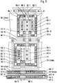
- Fig. 10 is a view showing a layout example of a protective circuit shown in Fig. 7.
- Fig. 11 is a view showing an arrangement of the analog switch shown in Fig. 7 in a chip.
- Fig. 12 is a circuit diagram showing a second embodiment of a semiconductor device of the present invention.
- Fig. 13 is a view showing a layout example of a NOR type output circuit shown in Fig. 12.
- Fig. 7 is a circuit diagram showing the first embodiment of the semiconductor device of the present invention.
- the semiconductor device is composed of a bonding pad 1, which is for performing signal inputting and outputting, an analog switch 30, which is for transmitting analog signals between the bonding pad 1 and the other pads (not shown) or between the bonding pad 1 and an internal analog circuit (not shown), and a protective circuit 20, which is for protecting the analog switch 30.
- a signal input from an analog signal 9 is transmitted through the analog switch 30 and the protective circuit 20 to the bonding pad 1, a signal input from the bonding pad 1 is transmitted through the protective circuit 20 and the analog switch 30 to the analog signal 9, and so on.
- the analog switch 30 is provided with a P type transfer gate 4 as a P type MOS transistor and an N type transfer gate 5 as an N type MOS transistor, to whose gate terminals reverse phase control signals 10 are respectively input by inverters 6a and 6b, a P type dummy transistor 11 with its drain terminal connected to a P type diffusion layer in the external side of the P type transfer gate 4 and its gate and source terminals connected to a power supply potential, and an N type dummy transistor 12 with its drain terminal connected to an N type diffusion layer in the external side of the N type transfer gate 5 and its gate and source terminals connected to a ground potential.
- the protective circuit 20 is provided with a P type protective transistor 2 as a P type protective transistor with its source and gate terminals connected to a power supply potential 7 and its drain terminal connected to the bonding pad 1, and an N type protective transistor 3 as an N type protective transistor with its source and gate terminals connected to the ground potential and its drain terminal connected to the bonding pad 1.
- Fig. 8 is a view showing a layout example of the analog switch 30 shown in Fig. 7.
- Fig. 9(a) is a section view taken along the line A-A' of the analog switch 30 shown in Fig. 8
- Fig. 9(b) is a section view taken along the line B-B' of the analog switch 30 shown in Fig. 8.
- Fig. 10 is a view showing a layout example of the protective circuit 20 shown in Fig. 7.
- the bonding pad 1 is connected through a second layer metallic wiring 101-1 and first layer metallic wirings 102-1 and 102-4 to the N type diffusion layers 104-1 and 104-3 of the N type transfer gate 4 and the P type diffusion layers 103-2 and 103-4 of the P type transfer gate 5. In this manner, the bonding pad 1 and the analog switch 130 are connected to each other.
- the N type diffusion layer 104-2 in the inner side of the N type transfer gate 4 and the P type diffusion layer 103-3 in the inner side of the P type transfer gate 5 are connected through a first layer metallic wiring 102-7 to an internal circuit.
- N type diffusion layer 104-1 of the N type transfer gate 5 in a side opposite an N type diffusion layer 104-2, which is connected to the inside of the N type diffusion layer 104-1, there is laid out an N type dummy transistor, which shares the N type diffusion layer 104-1 as a drain and uses a gate electrode 105-3 and an N type diffusion layer 104-6 connected through a first layer metallic wiring 102-3 to a ground potential as a gate and a source respectively.
- N type diffusion layer 104-3 of the N type transfer gate 5 in a side opposite the N type diffusion layer 104-2, which is connected to the inside of the N type diffusion layer 104-3, there is laid out an N type dummy transistor, which shares the N type diffusion layer 104-3 as a drain and uses a gate electrode 105-4 and an N type diffusion layer 104-7 connected through a first layer metallic wiring 102-2 to the ground potential as a gate and a source respectively.
- the N type diffusion layers 104-1 and 104-3 as the drains of the N type dummy transistors have the same structures as those of the N type diffusion layers 104-1 and 104-3 as the drains of the N type protective transistors shown in Fig. 10.
- P type diffusion layer 103-2 of the P type transfer gate 4 in a side opposite a P type diffusion layer 103-3 connected to the inside of the P type diffusion layer 103-2, there is laid out a P type dummy transistor, which shares the P type diffusion layer 103-2 as a drain and uses a gate electrode 106-3 and a P type diffusion layer 103-6 connected through a first layer metallic wiring 102-5 to a power supply potential as a gate and source respectively .
- a P type diffusion layer 103-4 of the P type transfer gate 4 in a side opposite the P type diffusion layer 103-3 connected to the inside of the P type diffusion layer 103-4, there is laid out a P type dummy transistor, which shares the P type diffusion layer 103-4 as a drain and uses a gate electrode 106-4 and a P type diffusion layer 103-7 connected through a first metallic wiring 102-6 to the power supply potential as a gate and a source respectively.
- the P type diffusion layers 103-2 and 103-4 as the drains of the P type dummy transistors have the same structures as those of the P type diffusion layers 103-2 and 103-4 as the drains of the P type protective transistors shown in Fig. 10.
- the N type transfer gate 5 is surrounded by a P type diffusion layer 103-1, which is connected to a ground potential (Vss) 8. Also, the P type transfer gate 4 is surrounded by an N type diffusion layer 104-4, which is connected to a power supply potential (Vdd) 7.
- Fig. 11 is a view showing the arrangement of the analog switch shown in Fig. 7 in a chip.
- the analog switch 30 is, as in the case of the protective circuit 20, arranged in a buffer region 200 divided from an internal region 220 by a guard ring 210.
- the diffusion layers are not destroyed by the concentration of current, and thus a high protective capability against excessive voltage from the outside is provided.
- the P type and N type dummy transistors 11 and 12 function, when an excessive voltage is applied from the outside, so as to turn away the excessive voltage to the power source and the ground as in the case of the P type and N type protective transistors 2 and 3.
- Fig. 12 is a circuit diagram showing a second embodiment of a semiconductor device of the present invention.
- the semiconductor device is composed of a NOR type output circuit 40 and a protective circuit 20, which is for protecting the NOR type output circuit 40.
- a signal input from a data signal 18 is transmitted through the NOR type output circuit 40 and the protective circuit 20 to the bonding pad 1, a signal input from the bonding pad 1 is transmitted through the protective circuit 20 and the NOR type output circuit 40 to the data signal 18, and so on.
- the NOR type output circuit 40 is provided with P type and N type transistors 13 and 16, which are connected to a control signal 17, P type and N type transistors 14 and 15, which are connected to the data signal 18, and a P type dummy transistor 19 with its gate and source terminals connected to a power supply potential 7 and its drain terminal connected to the protective circuit 20.
- the protective circuit 20 is provided with a P type protective transistor 2 with its source and gate terminals connected to the power supply potential 7 and its drain terminal connected to the bonding pad 1, and an N type protective transistor 3 with its source and gate terminals connected to a ground potential and its drain terminal connected to the bonding pad 1.
- Fig. 13 is a view showing a layout example of the NOR type output circuit 40 shown in Fig. 12.
- an excessive voltage from the outside is made to flow through the P type dummy transistor 19 to a power source and an ESD protective capability can be increased without breaking down the P type transistor.
- NOR type output circuit which was is formed by connecting the two P type transistors 13 and 14 to each other in series between the power supply potential and the pad.
- the present invention is not limited to the NOR type output circuit.
- the same effect can be obtained by a circuit which has two or more P type transistors connected in series between the power supply potential and the pad, or a circuit which has two or more N type transistors connected in series between the pad and the ground potential, for instance a NAND type output circuit with two N type transistors connected in series between the pad and the ground potential.
- the present invention since in a spot, in which the diffusion layer ends divided by the gate of the MOS transistor are connected to the pad, there is provided a dummy transistor with the diffusion layer used as a drain and with its gate and source connected to the ground potential or the power supply potential, if an excessive voltage of static electricity or the like, is applied through the pad to the semiconductor device, an excessive current is made to flow to the power source or the ground by the dummy transistor, and thereby the occurrence of a breakdown at a voltage lower than the breakdown voltage of the protective transistor can be prevented. As a result, it is possible to prevent the breakdown of the MOS transistor.
Landscapes
- Semiconductor Integrated Circuits (AREA)
- Metal-Oxide And Bipolar Metal-Oxide Semiconductor Integrated Circuits (AREA)
- Insulated Gate Type Field-Effect Transistor (AREA)
Applications Claiming Priority (3)
| Application Number | Priority Date | Filing Date | Title |
|---|---|---|---|
| JP103037/96 | 1996-04-25 | ||
| JP10303796 | 1996-04-25 | ||
| JP8103037A JP2914292B2 (ja) | 1996-04-25 | 1996-04-25 | 半導体装置 |
Publications (2)
| Publication Number | Publication Date |
|---|---|
| EP0803908A2 true EP0803908A2 (de) | 1997-10-29 |
| EP0803908A3 EP0803908A3 (de) | 2000-02-16 |
Family
ID=14343473
Family Applications (1)
| Application Number | Title | Priority Date | Filing Date |
|---|---|---|---|
| EP97106484A Withdrawn EP0803908A3 (de) | 1996-04-25 | 1997-04-18 | Halbleiteranordnung mit einer Schutzvorrichtung |
Country Status (5)
| Country | Link |
|---|---|
| US (1) | US5905287A (de) |
| EP (1) | EP0803908A3 (de) |
| JP (1) | JP2914292B2 (de) |
| KR (1) | KR100249716B1 (de) |
| CN (1) | CN1087103C (de) |
Cited By (1)
| Publication number | Priority date | Publication date | Assignee | Title |
|---|---|---|---|---|
| CN101236965B (zh) * | 2007-02-01 | 2011-05-11 | 瑞萨电子株式会社 | 半导体集成电路装置 |
Families Citing this family (29)
| Publication number | Priority date | Publication date | Assignee | Title |
|---|---|---|---|---|
| US6097066A (en) * | 1997-10-06 | 2000-08-01 | Taiwan Semiconductor Manufacturing Co., Ltd. | Electro-static discharge protection structure for semiconductor devices |
| JP3430080B2 (ja) * | 1999-10-08 | 2003-07-28 | Necエレクトロニクス株式会社 | 半導体装置及びその製造方法 |
| JP3495031B2 (ja) * | 2002-05-28 | 2004-02-09 | 沖電気工業株式会社 | 半導体装置の静電破壊防止保護回路 |
| US7179691B1 (en) | 2002-07-29 | 2007-02-20 | Taiwan Semiconductor Manufacturing Co., Ltd. | Method for four direction low capacitance ESD protection |
| US6798022B1 (en) * | 2003-03-11 | 2004-09-28 | Oki Electric Industry Co., Ltd. | Semiconductor device with improved protection from electrostatic discharge |
| US7908578B2 (en) * | 2007-08-02 | 2011-03-15 | Tela Innovations, Inc. | Methods for designing semiconductor device with dynamic array section |
| US8653857B2 (en) | 2006-03-09 | 2014-02-18 | Tela Innovations, Inc. | Circuitry and layouts for XOR and XNOR logic |
| US8658542B2 (en) | 2006-03-09 | 2014-02-25 | Tela Innovations, Inc. | Coarse grid design methods and structures |
| US7446352B2 (en) | 2006-03-09 | 2008-11-04 | Tela Innovations, Inc. | Dynamic array architecture |
| US8448102B2 (en) | 2006-03-09 | 2013-05-21 | Tela Innovations, Inc. | Optimizing layout of irregular structures in regular layout context |
| US7956421B2 (en) | 2008-03-13 | 2011-06-07 | Tela Innovations, Inc. | Cross-coupled transistor layouts in restricted gate level layout architecture |
| US8839175B2 (en) | 2006-03-09 | 2014-09-16 | Tela Innovations, Inc. | Scalable meta-data objects |
| US9563733B2 (en) | 2009-05-06 | 2017-02-07 | Tela Innovations, Inc. | Cell circuit and layout with linear finfet structures |
| US8541879B2 (en) | 2007-12-13 | 2013-09-24 | Tela Innovations, Inc. | Super-self-aligned contacts and method for making the same |
| US7763534B2 (en) | 2007-10-26 | 2010-07-27 | Tela Innovations, Inc. | Methods, structures and designs for self-aligning local interconnects used in integrated circuits |
| US9230910B2 (en) | 2006-03-09 | 2016-01-05 | Tela Innovations, Inc. | Oversized contacts and vias in layout defined by linearly constrained topology |
| TWI296150B (en) * | 2006-04-25 | 2008-04-21 | Siliconmotion Inc | An analog input/output circuit with esd protection |
| US8667443B2 (en) | 2007-03-05 | 2014-03-04 | Tela Innovations, Inc. | Integrated circuit cell library for multiple patterning |
| US8453094B2 (en) | 2008-01-31 | 2013-05-28 | Tela Innovations, Inc. | Enforcement of semiconductor structure regularity for localized transistors and interconnect |
| US7939443B2 (en) | 2008-03-27 | 2011-05-10 | Tela Innovations, Inc. | Methods for multi-wire routing and apparatus implementing same |
| KR101761530B1 (ko) | 2008-07-16 | 2017-07-25 | 텔라 이노베이션스, 인코포레이티드 | 동적 어레이 아키텍쳐에서의 셀 페이징과 배치를 위한 방법 및 그 구현 |
| US8661392B2 (en) | 2009-10-13 | 2014-02-25 | Tela Innovations, Inc. | Methods for cell boundary encroachment and layouts implementing the Same |
| US9159627B2 (en) | 2010-11-12 | 2015-10-13 | Tela Innovations, Inc. | Methods for linewidth modification and apparatus implementing the same |
| CN102569400B (zh) * | 2011-12-13 | 2014-11-05 | 钜泉光电科技(上海)股份有限公司 | 金属氧化物半导体器件 |
| US9613952B2 (en) * | 2014-07-25 | 2017-04-04 | Macronix International Co., Ltd. | Semiconductor ESD protection device |
| CN105846804A (zh) * | 2016-03-24 | 2016-08-10 | 天津理工大学 | 基于多路选通的高压测量开关电路 |
| CN106961215B (zh) * | 2017-05-12 | 2019-01-22 | 金戈 | 一种具有瞬时纠正功能的高效率非反Buck-boost变压芯片 |
| US10692808B2 (en) | 2017-09-18 | 2020-06-23 | Qualcomm Incorporated | High performance cell design in a technology with high density metal routing |
| TWI894425B (zh) * | 2022-01-18 | 2025-08-21 | 聯華電子股份有限公司 | 具有背部穿矽孔的半導體結構及其得出晶粒識別碼的方法 |
Citations (1)
| Publication number | Priority date | Publication date | Assignee | Title |
|---|---|---|---|---|
| JPH0823269A (ja) * | 1994-07-06 | 1996-01-23 | Toshiba Corp | アナログスイッチ回路 |
Family Cites Families (15)
| Publication number | Priority date | Publication date | Assignee | Title |
|---|---|---|---|---|
| US4609931A (en) * | 1981-07-17 | 1986-09-02 | Tokyo Shibaura Denki Kabushiki Kaisha | Input protection MOS semiconductor device with zener breakdown mechanism |
| JP2573574B2 (ja) * | 1986-06-03 | 1997-01-22 | ソニー株式会社 | 出力バッファ回路 |
| JP2598446B2 (ja) * | 1988-01-21 | 1997-04-09 | パイオニア株式会社 | Mis−fet |
| JPH01236731A (ja) * | 1988-03-16 | 1989-09-21 | Nec Corp | 相補型アナログスイッチ |
| JPH024011A (ja) * | 1988-06-21 | 1990-01-09 | Nec Corp | アナログスイッチ回路 |
| JPH0282570A (ja) * | 1988-09-19 | 1990-03-23 | Nec Corp | 半導体装置 |
| JP2633746B2 (ja) * | 1991-05-27 | 1997-07-23 | 株式会社東芝 | 半導体装置 |
| JPH05326865A (ja) * | 1992-05-14 | 1993-12-10 | Nec Corp | 半導体集積回路装置 |
| JPH0661439A (ja) * | 1992-05-18 | 1994-03-04 | Nec Corp | 半導体集積回路装置 |
| JPH07122650A (ja) * | 1993-10-22 | 1995-05-12 | Yamaha Corp | 半導体装置 |
| JPH07161926A (ja) * | 1993-12-02 | 1995-06-23 | Mitsubishi Electric Corp | アナログ信号切替え回路 |
| JP3447372B2 (ja) * | 1994-06-13 | 2003-09-16 | 富士通株式会社 | 半導体装置 |
| JPH0837284A (ja) * | 1994-07-21 | 1996-02-06 | Nippondenso Co Ltd | 半導体集積回路装置 |
| JPH0837238A (ja) * | 1994-07-21 | 1996-02-06 | Hitachi Ltd | 半導体集積回路装置 |
| US5714784A (en) * | 1995-10-19 | 1998-02-03 | Winbond Electronics Corporation | Electrostatic discharge protection device |
-
1996
- 1996-04-25 JP JP8103037A patent/JP2914292B2/ja not_active Expired - Fee Related
-
1997
- 1997-04-17 US US08/837,344 patent/US5905287A/en not_active Expired - Fee Related
- 1997-04-18 EP EP97106484A patent/EP0803908A3/de not_active Withdrawn
- 1997-04-24 CN CN97111732A patent/CN1087103C/zh not_active Expired - Fee Related
- 1997-04-25 KR KR1019970015689A patent/KR100249716B1/ko not_active Expired - Fee Related
Patent Citations (1)
| Publication number | Priority date | Publication date | Assignee | Title |
|---|---|---|---|---|
| JPH0823269A (ja) * | 1994-07-06 | 1996-01-23 | Toshiba Corp | アナログスイッチ回路 |
Cited By (1)
| Publication number | Priority date | Publication date | Assignee | Title |
|---|---|---|---|---|
| CN101236965B (zh) * | 2007-02-01 | 2011-05-11 | 瑞萨电子株式会社 | 半导体集成电路装置 |
Also Published As
| Publication number | Publication date |
|---|---|
| CN1087103C (zh) | 2002-07-03 |
| KR100249716B1 (ko) | 2000-03-15 |
| JP2914292B2 (ja) | 1999-06-28 |
| KR970072397A (ko) | 1997-11-07 |
| US5905287A (en) | 1999-05-18 |
| EP0803908A3 (de) | 2000-02-16 |
| JPH09293832A (ja) | 1997-11-11 |
| CN1175091A (zh) | 1998-03-04 |
Similar Documents
| Publication | Publication Date | Title |
|---|---|---|
| US5905287A (en) | Semiconductor device with high voltage protection | |
| US4876584A (en) | Electrostatic discharge protection circuit | |
| EP0412561B1 (de) | Integrierte Halbleiterschaltungsanordnung | |
| US7049663B2 (en) | ESD protection device with high voltage and negative voltage tolerance | |
| US4543593A (en) | Semiconductor protective device | |
| JPH088391A (ja) | 半導体回路 | |
| US5036215A (en) | Pass gate multiplexer receiver circuit | |
| US6266222B1 (en) | ESD protection network for circuit structures formed in a semiconductor | |
| KR100387189B1 (ko) | 절연체상반도체장치및그보호회로 | |
| KR100301538B1 (ko) | 반도체장치 | |
| JP3559075B2 (ja) | Cmos技術の集積電子回路用の極性反転保護装置 | |
| KR970004452B1 (ko) | 정전보호회로 | |
| US6680512B2 (en) | Semiconductor device having an integral protection circuit | |
| US6833590B2 (en) | Semiconductor device | |
| US6583475B2 (en) | Semiconductor device | |
| US5276371A (en) | Output buffer having high resistance against electrostatic breakdown | |
| CA1289267C (en) | Latchup and electrostatic discharge protection structure | |
| KR100270949B1 (ko) | 극성에 상관없이 내부 회로를 보호하기 위하여 전원 공급 단자들 사이에 적용한 정전기 방지 회로 | |
| US6538291B1 (en) | Input protection circuit | |
| KR19990063375A (ko) | 번인 동작 동안 백 게이트 전압을 사용하는 집적 회로 및 그 제조 방법 | |
| US7723794B2 (en) | Load driving device | |
| JP3288545B2 (ja) | 半導体装置 | |
| KR0169359B1 (ko) | 반도체 장치의 보호 소자 | |
| JP3442331B2 (ja) | 半導体装置 | |
| EP0620598B1 (de) | Eingangs-/ausgangsschutzschaltung |
Legal Events
| Date | Code | Title | Description |
|---|---|---|---|
| PUAI | Public reference made under article 153(3) epc to a published international application that has entered the european phase |
Free format text: ORIGINAL CODE: 0009012 |
|
| AK | Designated contracting states |
Kind code of ref document: A2 Designated state(s): DE FR GB |
|
| PUAL | Search report despatched |
Free format text: ORIGINAL CODE: 0009013 |
|
| AK | Designated contracting states |
Kind code of ref document: A3 Designated state(s): DE FR GB |
|
| 17P | Request for examination filed |
Effective date: 20000122 |
|
| RAP1 | Party data changed (applicant data changed or rights of an application transferred) |
Owner name: NEC ELECTRONICS CORPORATION |
|
| 17Q | First examination report despatched |
Effective date: 20040616 |
|
| GRAP | Despatch of communication of intention to grant a patent |
Free format text: ORIGINAL CODE: EPIDOSNIGR1 |
|
| STAA | Information on the status of an ep patent application or granted ep patent |
Free format text: STATUS: THE APPLICATION IS DEEMED TO BE WITHDRAWN |
|
| 18D | Application deemed to be withdrawn |
Effective date: 20051119 |