EP0803908A2 - Semiconductor device including protection means - Google Patents
Semiconductor device including protection means Download PDFInfo
- Publication number
- EP0803908A2 EP0803908A2 EP97106484A EP97106484A EP0803908A2 EP 0803908 A2 EP0803908 A2 EP 0803908A2 EP 97106484 A EP97106484 A EP 97106484A EP 97106484 A EP97106484 A EP 97106484A EP 0803908 A2 EP0803908 A2 EP 0803908A2
- Authority
- EP
- European Patent Office
- Prior art keywords
- type
- transistor
- gate
- protective
- pads
- Prior art date
- Legal status (The legal status is an assumption and is not a legal conclusion. Google has not performed a legal analysis and makes no representation as to the accuracy of the status listed.)
- Withdrawn
Links
Images


Classifications
-
- H—ELECTRICITY
- H10—SEMICONDUCTOR DEVICES; ELECTRIC SOLID-STATE DEVICES NOT OTHERWISE PROVIDED FOR
- H10D—INORGANIC ELECTRIC SEMICONDUCTOR DEVICES
- H10D84/00—Integrated devices formed in or on semiconductor substrates that comprise only semiconducting layers, e.g. on Si wafers or on GaAs-on-Si wafers
- H10D84/80—Integrated devices formed in or on semiconductor substrates that comprise only semiconducting layers, e.g. on Si wafers or on GaAs-on-Si wafers characterised by the integration of at least one component covered by groups H10D12/00 or H10D30/00, e.g. integration of IGFETs
- H10D84/82—Integrated devices formed in or on semiconductor substrates that comprise only semiconducting layers, e.g. on Si wafers or on GaAs-on-Si wafers characterised by the integration of at least one component covered by groups H10D12/00 or H10D30/00, e.g. integration of IGFETs of only field-effect components
-
- H—ELECTRICITY
- H10—SEMICONDUCTOR DEVICES; ELECTRIC SOLID-STATE DEVICES NOT OTHERWISE PROVIDED FOR
- H10D—INORGANIC ELECTRIC SEMICONDUCTOR DEVICES
- H10D89/00—Aspects of integrated devices not covered by groups H10D84/00 - H10D88/00
- H10D89/60—Integrated devices comprising arrangements for electrical or thermal protection, e.g. protection circuits against electrostatic discharge [ESD]
- H10D89/601—Integrated devices comprising arrangements for electrical or thermal protection, e.g. protection circuits against electrostatic discharge [ESD] for devices having insulated gate electrodes, e.g. for IGFETs or IGBTs
- H10D89/811—Integrated devices comprising arrangements for electrical or thermal protection, e.g. protection circuits against electrostatic discharge [ESD] for devices having insulated gate electrodes, e.g. for IGFETs or IGBTs using FETs as protective elements
-
- H—ELECTRICITY
- H02—GENERATION; CONVERSION OR DISTRIBUTION OF ELECTRIC POWER
- H02H—EMERGENCY PROTECTIVE CIRCUIT ARRANGEMENTS
- H02H9/00—Emergency protective circuit arrangements for limiting excess current or voltage without disconnection
- H02H9/04—Emergency protective circuit arrangements for limiting excess current or voltage without disconnection responsive to excess voltage
- H02H9/045—Emergency protective circuit arrangements for limiting excess current or voltage without disconnection responsive to excess voltage adapted to a particular application and not provided for elsewhere
- H02H9/046—Emergency protective circuit arrangements for limiting excess current or voltage without disconnection responsive to excess voltage adapted to a particular application and not provided for elsewhere responsive to excess voltage appearing at terminals of integrated circuits
Definitions
- the present invention relates to a semiconductor integrated circuit, and more particularly to a transfer gate which uses an insulated gate electric field effect transistor (referred to as a MOS transistor, hereinafter).
- MOS transistor insulated gate electric field effect transistor
- Fig. 1 is a circuit diagram showing one constitutional example of a conventional semiconductor device.
- this conventional semiconductor device is composed of an analog switch 130, which is for transmitting an analog signal from an input pad to an output pad, and a protective circuit 20, which is for protecting the analog switch 130.
- a signal input from an analog signal 9 is transmitted through the analog switch 130 and the protective circuit 20 to a bonding pad 1
- a signal input from the bonding pad 1 is transmitted through the protective circuit 20 and the analog switch 130 to the analog signal 9, and so on.
- the analog switch 130 there are provided side by side a P type transfer gate 4 and an N type transfer gate 5, to whose gate terminals reverse phase control signals 10 are input by inverters 6a and 6b respectively.
- a P type protective transistor 2 with its source and gate terminals connected to a power supply potential 7 and its drain terminal connected to the bonding pad 1, and an N type protective transistor 3, with its source and gate terminals connected to a ground potential and its drain terminal connected to the bonding pad 1.
- Fig. 2 is a view showing a layout example of the analog switch 130 shown in Fig. 1.
- Fig. 3(a) is a section view taken along the line C-C' of the analog switch 130 shown in Fig. 2
- Fig. 3(b) is a section view taken along the line D-D' of the analog switch 130 shown in Fig. 2.
- the bonding pad 1 is connected through a second layer metallic wiring 101-1 and first layer metallic wirings 102-1 and 102-4 to the N type diffusion layers 104-1 and 104-3 of the N type transfer gate 4 and to the P type diffusion layers 103-2 and 103-4 of the P type transfer gate 5. Thereby, the bonding pad 1 and the analog switch 130 are interconnected.
- an N type diffusion layer 104-2 in the internal side of the N type transfer gate 5 and a P type diffusion layer 103-3 in the internal side of the P type transfer gate 4 are connected through a first layer metallic wiring 102-7 to an internal circuit.
- the N type transfer gate 5 is surrounded by a P type diffusion layer 103-1, which is connected to a ground potential (Vss) 8. Also, the P type transfer gate 4 is surrounded by an N type diffusion layer 104-4, which is connected to the power supply potential (Vdd) 7.
- the P type transfer gate 4 and the N type transfer gate 5 are both made to be non-conductive, and thus the outside and the inside of the chip are electrically shielded from each other.
- the P type transfer gate 4 and the N type transfer gate 5 are both made to be conductive, and thus a signal having an optional potential between the ground potential 8 and the power supply potential 7 is transmitted from the external bonding pad 1 to the internal analog signal 9, or from the internal analog signal 9 to the external bonding pad 1.
- a breakdown voltage in this case will be referred to as BVDS.
- the N type diffusion layer of the source terminal and a diode is formed by the P type well are forward biased, a parasitic NPN type bipolar transistor is formed by the drain terminal, the P type well and the source terminal is made to be in an operation state (referred to as a snapback operation state, hereinafter), and an excessive current coming from the outside is made to flow to the ground.
- a potential for the drain terminal of the N type protective transistor 3 is fixed at a value lower than that of the breakdown voltage of the N type diffusion layer, which has been connected to the bonding pad 1 of the N type transfer gate 5, and thereby the analog switch 130 is prevented from being broken down.
- the P type diffusion layer of the source terminal and a diode is formed by the N type well are forward biased, a parasitic PNP type bipolar transistor is formed by the drain terminal, the N type well and the source terminal are made to be in a snapback operatation state and thus an excessive current coming from the outside is made to flow to the poser source.
- a potential for the drain terminal of the P type protective transistor is fixed at a value lower than that of the breakdown voltage of the P type diffusion layer, which has been connected to the bonding pad 1 of the P type transfer gate 4, and thereby the analog switch is prevented from being broken down.
- Fig. 4 is a circuit diagram showing another constitutional example of a conventional semiconductor device.
- the conventional semiconductor device of this example is composed of a NOR type output circuit 140, and a protective circuit 20, which is for protecting the NOR type output circuit 140.
- a signal input from a data signal 18 is transmitted through the NOR type output circuit 140 and the protective circuit 20 to a bonding pad 1, a signal input from the bonding pad 1 is transmitted through the protective circuit 20 and the NOR type output circuit 140 to the data signal 18, and so on.
- the NOR type output circuit 140 there are provided a P type transistor 13 and an N type transistor 16, which are connected to a control signal 17, and P type transistor 14 and an N type transistor 15, which are connected to the data signal 18.
- a P type protective transistor 2 with its source and gate terminals connected to a power supply potential 7 and its drain terminal connected to the bonding pad 1
- an N type protective transistor 3 with its source and gate terminals connected to a ground potential and its drain terminal connected to the bonding pad 1.
- Fig. 5 is a view showing the layout example of a NOR type outout circuit shown in Fig. 4.
- a P type diffusion layer 103-4 in the drain part of a vertically placed P type transistor is connected to the pad through a first layer metallic wiring 102-1, a contact C2 between first and second layer metallic wirings and a second layer metallic wiring 101-1.
- the drain terminal of the N type protective transistor 3 and the N type diffusion layer of the N type transfer gate 5 are almost at the same potential, because these are interconnected by a low resistant metallic wiring.
- a breakdown voltage in this case will be referred to as BVJ.
- BVJ depends on the layout of the analog switch.
- Fig. 6 is a view showing a breakdown voltage for the semiconductor device shown in Fig. 2.
- a BVJ 1 is a breakdown voltage when the diffusion layer end of a certain side does not intersect that of another side as in the case of the N type diffusion layer 104-2 shown in Fig. 2.
- a BVJ 2 is a breakdown voltage when the diffusion layer end of a certain side intersects that of another diffusion layer as in the case of the N type diffusion layers 104-1 and 104-3.
- a BVDS is a breakdown voltage for the N type protective transistor 3.
- the BVJ 2 is lower than the BVJ 1, which is a breakdown voltage when there are no corner parts in the diffusion layers.
- the present invention was made in light of the foregoing problem inherent in the prior art, and it is an object of the invention to provide a semiconductor device, which has a high protective capability against an excessive voltage applied from the outside.
- the object of the present invention is achieved by a semiconductor device, which comprises a plurality of pads for performing signal inputting and outputting, an analog switch having P type and N type MOS transistors for transmitting signals among the pads or between the pads and an internal analog circuit and a protective circuit having P type and N type protective MOS transistors for protecting the analog switch, the analog switch being provided in a spot, in which diffusion layer ends divided by the gate of the N type MOS transistor are connected to the pads, an N type dummy transistor formed by using the diffusion layers as drains and connecting a gate and a source to a ground potential.
- the object of the present invention is also achieved by a semiconductor device, which comprises a plurality of pads for performing signal inputting and outputting, an analog switch having P type and N type MOS transistors for transmitting signals among the pads or between the pads and an internal analog circuit and a protective circuit having P type and N type protective MOS transistors for protecting the analog switch, the analog switch being provided in a spot, in which diffusion layer ends divided by the gate of the P type MOS transistor are connected to the pads, a P type dummy transistor is formed by using the diffusion layers as drains and connecting a gate and a source to a power supply potential and the dummy transistor having the same structure as that of the protective MOS transistor.
- the object of the present invention is further achieved by a semiconductor device, which comprises a plurality of pads for performing signal inputting and outputting, an output circuit having two or more P type MOS transistors connected in series between a power supply potential and the pads and a protective circuit having P type and N type protective MOS transistors for protecting the output circuit, the output circuit being provided in a spot, in which diffusion layer ends divided by the gates of the P type MOS transistors are connected to the pads, a P type dummy transistor is formed by using the diffusion layers as drains and connecting a gate and a source to the power supply potential and the output circuit being a NOR type output circuit.
- a semiconductor device which comprises a plurality of pads for performing signal inputting and outputting, an output circuit having two or more N type MOS transistors connected in series between a ground potential and the pads and a protective circuit having P type and N type protective MOS transistors for protecting the output circuit, the output circuit being provided with in a spot, in which diffusion layer ends divided by the gates of the N type MOS transistors are connected to the pads, an N type dummy transistor is formed by using the diffusion layers as drains and connecting a gate and a source to the ground potential, the output circuit being a NAND type output circuit and the dummy transistor having the same structure as that of the protective MOS transistor.
- the present invention which provides a semiconductor device thus constructed, when an excessive voltage of static electricity or the like, is applied through the pads to the semiconductor device, an excessive current is made to flow to the ground by the dummy transistor, and thereby the occurrence of a breakdown at a voltage lower than the breakdown voltage of the protective transistor can be prevented and the breakdown of the MOS transistor can be prevented.
- Fig. 1 is a circuit diagram showing one constitutional example of a conventional semiconductor device.
- Fig. 2 is a view showing a layout example of an analog switch shown in Fig. 1.
- Fig. 3(a) is a section view taken along a line C-C' of the analog switch shown in Fig. 2.
- Fig. 3(b) is a section view taken along a line D-D' of the analog switch shown in Fig. 2.
- Fig. 4 is a circuit diagram showing another constitutional example of a conventional semiconductor device.
- Fig. 5 is a view showing a layout example of an analog switch shown in Fig. 4.
- Fig. 6 is a view showing a breakdown voltage of the semiconductor device shown in Fig. 2.
- Fig. 7 is a circuit diagram showing a first embodiment of a semiconductor device of the present invention.
- Fig. 8 is a view showing a layout example of an analog switch shown in Fig. 7.
- Fig. 9(a) is a section view taken along a line A-A' of the analog switch shown in Fig. 8.
- Fig. 9(b) is a section view taken along a line B-B' of the analog switch shown in Fig. 8.
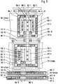
- Fig. 10 is a view showing a layout example of a protective circuit shown in Fig. 7.
- Fig. 11 is a view showing an arrangement of the analog switch shown in Fig. 7 in a chip.
- Fig. 12 is a circuit diagram showing a second embodiment of a semiconductor device of the present invention.
- Fig. 13 is a view showing a layout example of a NOR type output circuit shown in Fig. 12.
- Fig. 7 is a circuit diagram showing the first embodiment of the semiconductor device of the present invention.
- the semiconductor device is composed of a bonding pad 1, which is for performing signal inputting and outputting, an analog switch 30, which is for transmitting analog signals between the bonding pad 1 and the other pads (not shown) or between the bonding pad 1 and an internal analog circuit (not shown), and a protective circuit 20, which is for protecting the analog switch 30.
- a signal input from an analog signal 9 is transmitted through the analog switch 30 and the protective circuit 20 to the bonding pad 1, a signal input from the bonding pad 1 is transmitted through the protective circuit 20 and the analog switch 30 to the analog signal 9, and so on.
- the analog switch 30 is provided with a P type transfer gate 4 as a P type MOS transistor and an N type transfer gate 5 as an N type MOS transistor, to whose gate terminals reverse phase control signals 10 are respectively input by inverters 6a and 6b, a P type dummy transistor 11 with its drain terminal connected to a P type diffusion layer in the external side of the P type transfer gate 4 and its gate and source terminals connected to a power supply potential, and an N type dummy transistor 12 with its drain terminal connected to an N type diffusion layer in the external side of the N type transfer gate 5 and its gate and source terminals connected to a ground potential.
- the protective circuit 20 is provided with a P type protective transistor 2 as a P type protective transistor with its source and gate terminals connected to a power supply potential 7 and its drain terminal connected to the bonding pad 1, and an N type protective transistor 3 as an N type protective transistor with its source and gate terminals connected to the ground potential and its drain terminal connected to the bonding pad 1.
- Fig. 8 is a view showing a layout example of the analog switch 30 shown in Fig. 7.
- Fig. 9(a) is a section view taken along the line A-A' of the analog switch 30 shown in Fig. 8
- Fig. 9(b) is a section view taken along the line B-B' of the analog switch 30 shown in Fig. 8.
- Fig. 10 is a view showing a layout example of the protective circuit 20 shown in Fig. 7.
- the bonding pad 1 is connected through a second layer metallic wiring 101-1 and first layer metallic wirings 102-1 and 102-4 to the N type diffusion layers 104-1 and 104-3 of the N type transfer gate 4 and the P type diffusion layers 103-2 and 103-4 of the P type transfer gate 5. In this manner, the bonding pad 1 and the analog switch 130 are connected to each other.
- the N type diffusion layer 104-2 in the inner side of the N type transfer gate 4 and the P type diffusion layer 103-3 in the inner side of the P type transfer gate 5 are connected through a first layer metallic wiring 102-7 to an internal circuit.
- N type diffusion layer 104-1 of the N type transfer gate 5 in a side opposite an N type diffusion layer 104-2, which is connected to the inside of the N type diffusion layer 104-1, there is laid out an N type dummy transistor, which shares the N type diffusion layer 104-1 as a drain and uses a gate electrode 105-3 and an N type diffusion layer 104-6 connected through a first layer metallic wiring 102-3 to a ground potential as a gate and a source respectively.
- N type diffusion layer 104-3 of the N type transfer gate 5 in a side opposite the N type diffusion layer 104-2, which is connected to the inside of the N type diffusion layer 104-3, there is laid out an N type dummy transistor, which shares the N type diffusion layer 104-3 as a drain and uses a gate electrode 105-4 and an N type diffusion layer 104-7 connected through a first layer metallic wiring 102-2 to the ground potential as a gate and a source respectively.
- the N type diffusion layers 104-1 and 104-3 as the drains of the N type dummy transistors have the same structures as those of the N type diffusion layers 104-1 and 104-3 as the drains of the N type protective transistors shown in Fig. 10.
- P type diffusion layer 103-2 of the P type transfer gate 4 in a side opposite a P type diffusion layer 103-3 connected to the inside of the P type diffusion layer 103-2, there is laid out a P type dummy transistor, which shares the P type diffusion layer 103-2 as a drain and uses a gate electrode 106-3 and a P type diffusion layer 103-6 connected through a first layer metallic wiring 102-5 to a power supply potential as a gate and source respectively .
- a P type diffusion layer 103-4 of the P type transfer gate 4 in a side opposite the P type diffusion layer 103-3 connected to the inside of the P type diffusion layer 103-4, there is laid out a P type dummy transistor, which shares the P type diffusion layer 103-4 as a drain and uses a gate electrode 106-4 and a P type diffusion layer 103-7 connected through a first metallic wiring 102-6 to the power supply potential as a gate and a source respectively.
- the P type diffusion layers 103-2 and 103-4 as the drains of the P type dummy transistors have the same structures as those of the P type diffusion layers 103-2 and 103-4 as the drains of the P type protective transistors shown in Fig. 10.
- the N type transfer gate 5 is surrounded by a P type diffusion layer 103-1, which is connected to a ground potential (Vss) 8. Also, the P type transfer gate 4 is surrounded by an N type diffusion layer 104-4, which is connected to a power supply potential (Vdd) 7.
- Fig. 11 is a view showing the arrangement of the analog switch shown in Fig. 7 in a chip.
- the analog switch 30 is, as in the case of the protective circuit 20, arranged in a buffer region 200 divided from an internal region 220 by a guard ring 210.
- the diffusion layers are not destroyed by the concentration of current, and thus a high protective capability against excessive voltage from the outside is provided.
- the P type and N type dummy transistors 11 and 12 function, when an excessive voltage is applied from the outside, so as to turn away the excessive voltage to the power source and the ground as in the case of the P type and N type protective transistors 2 and 3.
- Fig. 12 is a circuit diagram showing a second embodiment of a semiconductor device of the present invention.
- the semiconductor device is composed of a NOR type output circuit 40 and a protective circuit 20, which is for protecting the NOR type output circuit 40.
- a signal input from a data signal 18 is transmitted through the NOR type output circuit 40 and the protective circuit 20 to the bonding pad 1, a signal input from the bonding pad 1 is transmitted through the protective circuit 20 and the NOR type output circuit 40 to the data signal 18, and so on.
- the NOR type output circuit 40 is provided with P type and N type transistors 13 and 16, which are connected to a control signal 17, P type and N type transistors 14 and 15, which are connected to the data signal 18, and a P type dummy transistor 19 with its gate and source terminals connected to a power supply potential 7 and its drain terminal connected to the protective circuit 20.
- the protective circuit 20 is provided with a P type protective transistor 2 with its source and gate terminals connected to the power supply potential 7 and its drain terminal connected to the bonding pad 1, and an N type protective transistor 3 with its source and gate terminals connected to a ground potential and its drain terminal connected to the bonding pad 1.
- Fig. 13 is a view showing a layout example of the NOR type output circuit 40 shown in Fig. 12.
- an excessive voltage from the outside is made to flow through the P type dummy transistor 19 to a power source and an ESD protective capability can be increased without breaking down the P type transistor.
- NOR type output circuit which was is formed by connecting the two P type transistors 13 and 14 to each other in series between the power supply potential and the pad.
- the present invention is not limited to the NOR type output circuit.
- the same effect can be obtained by a circuit which has two or more P type transistors connected in series between the power supply potential and the pad, or a circuit which has two or more N type transistors connected in series between the pad and the ground potential, for instance a NAND type output circuit with two N type transistors connected in series between the pad and the ground potential.
- the present invention since in a spot, in which the diffusion layer ends divided by the gate of the MOS transistor are connected to the pad, there is provided a dummy transistor with the diffusion layer used as a drain and with its gate and source connected to the ground potential or the power supply potential, if an excessive voltage of static electricity or the like, is applied through the pad to the semiconductor device, an excessive current is made to flow to the power source or the ground by the dummy transistor, and thereby the occurrence of a breakdown at a voltage lower than the breakdown voltage of the protective transistor can be prevented. As a result, it is possible to prevent the breakdown of the MOS transistor.
Landscapes
- Semiconductor Integrated Circuits (AREA)
- Metal-Oxide And Bipolar Metal-Oxide Semiconductor Integrated Circuits (AREA)
- Insulated Gate Type Field-Effect Transistor (AREA)
Abstract
Description
- The present invention relates to a semiconductor integrated circuit, and more particularly to a transfer gate which uses an insulated gate electric field effect transistor (referred to as a MOS transistor, hereinafter).
- Fig. 1 is a circuit diagram showing one constitutional example of a conventional semiconductor device.
- Referring to Fig. 1, this conventional semiconductor device is composed of an
analog switch 130, which is for transmitting an analog signal from an input pad to an output pad, and aprotective circuit 20, which is for protecting theanalog switch 130. A signal input from an analog signal 9 is transmitted through theanalog switch 130 and theprotective circuit 20 to abonding pad 1, a signal input from thebonding pad 1 is transmitted through theprotective circuit 20 and theanalog switch 130 to the analog signal 9, and so on. In theanalog switch 130, there are provided side by side a P type transfer gate 4 and an Ntype transfer gate 5, to whose gate terminals reversephase control signals 10 are input byinverters protective circuit 20, there are provided a P typeprotective transistor 2, with its source and gate terminals connected to apower supply potential 7 and its drain terminal connected to thebonding pad 1, and an N typeprotective transistor 3, with its source and gate terminals connected to a ground potential and its drain terminal connected to thebonding pad 1. - Fig. 2 is a view showing a layout example of the
analog switch 130 shown in Fig. 1. - Fig. 3(a) is a section view taken along the line C-C' of the
analog switch 130 shown in Fig. 2, and Fig. 3(b) is a section view taken along the line D-D' of theanalog switch 130 shown in Fig. 2. - Referring to Fig. 2, the
bonding pad 1 is connected through a second layer metallic wiring 101-1 and first layer metallic wirings 102-1 and 102-4 to the N type diffusion layers 104-1 and 104-3 of the N type transfer gate 4 and to the P type diffusion layers 103-2 and 103-4 of the Ptype transfer gate 5. Thereby, thebonding pad 1 and theanalog switch 130 are interconnected. - Herein, an N type diffusion layer 104-2 in the internal side of the N
type transfer gate 5 and a P type diffusion layer 103-3 in the internal side of the P type transfer gate 4 are connected through a first layer metallic wiring 102-7 to an internal circuit. - Furthermore, in order to prevent latching up, the N
type transfer gate 5 is surrounded by a P type diffusion layer 103-1, which is connected to a ground potential (Vss) 8. Also, the P type transfer gate 4 is surrounded by an N type diffusion layer 104-4, which is connected to the power supply potential (Vdd) 7. - The operation of the analog switch thus constructed will be described below.
- When a
control signal 10 is at a low level, the P type transfer gate 4 and the Ntype transfer gate 5 are both made to be non-conductive, and thus the outside and the inside of the chip are electrically shielded from each other. - When a
control signal 10 is at a high level, the P type transfer gate 4 and the Ntype transfer gate 5 are both made to be conductive, and thus a signal having an optional potential between theground potential 8 and thepower supply potential 7 is transmitted from theexternal bonding pad 1 to the internal analog signal 9, or from the internal analog signal 9 to theexternal bonding pad 1. - Next, the operation of the
protective circuit 20 for preventing the breakdown of the transistor, which constitutes theanalog switch 130, will be described. This breakdown occurs when an excessive voltage of static electricity and so on is applied from the outside. - When a positive excessive voltage is applied to the ground from the outside, first a breakdown occurs in the N type diffusion layer in the gate terminal side of the drain terminal of the N type
protective transistor 3 and thus a current is made to flow to a P type well. A breakdown voltage in this case will be referred to as BVDS. - Then, by lowering of the voltage caused by the current which has flown into the P type well, the N type diffusion layer of the source terminal and a diode is formed by the P type well are forward biased, a parasitic NPN type bipolar transistor is formed by the drain terminal, the P type well and the source terminal is made to be in an operation state (referred to as a snapback operation state, hereinafter), and an excessive current coming from the outside is made to flow to the ground.
- After the snapback operation state has been realized, a potential for the drain terminal of the N type
protective transistor 3 is fixed at a value lower than that of the breakdown voltage of the N type diffusion layer, which has been connected to thebonding pad 1 of the Ntype transfer gate 5, and thereby theanalog switch 130 is prevented from being broken down. - When a negative excessive voltage is applied to the ground from the outside, the drain diffusion layers of the N type
protective transistor 3 are forward biased, a current is made to flow to the ground through the P type well, and thereby theanalog switch 130 is prevented from being broken down. - When a positive excessive voltage is applied to the power source from the outside, the drain diffusion layers of the P type
protective transistor 2 are forward biased, a current is made to flow to the power source through an N type well, and thereby theanalog switch 130 is prevented from being broken down. - Also, when a negative excessive voltage is applied to the power source from the outside, first a breakdown occurs in the P type diffusion layer in the gate terminal side of the drain terminal of the P type
protective transistor 2, and thus a current is made to flow to the N type well. - Then, by lowering of the voltage caused by the current which has flown into the N type well, the P type diffusion layer of the source terminal and a diode is formed by the N type well are forward biased, a parasitic PNP type bipolar transistor is formed by the drain terminal, the N type well and the source terminal are made to be in a snapback operatation state and thus an excessive current coming from the outside is made to flow to the poser source.
- After the snapback operation state has been realized, a potential for the drain terminal of the P type protective transistor is fixed at a value lower than that of the breakdown voltage of the P type diffusion layer, which has been connected to the
bonding pad 1 of the P type transfer gate 4, and thereby the analog switch is prevented from being broken down. - Fig. 4 is a circuit diagram showing another constitutional example of a conventional semiconductor device.
- Referring to Fig. 4, the conventional semiconductor device of this example is composed of a NOR
type output circuit 140, and aprotective circuit 20, which is for protecting the NORtype output circuit 140. A signal input from adata signal 18 is transmitted through the NORtype output circuit 140 and theprotective circuit 20 to abonding pad 1, a signal input from thebonding pad 1 is transmitted through theprotective circuit 20 and the NORtype output circuit 140 to thedata signal 18, and so on. In the NORtype output circuit 140, there are provided aP type transistor 13 and anN type transistor 16, which are connected to acontrol signal 17, andP type transistor 14 and anN type transistor 15, which are connected to thedata signal 18. In theprotective circuit 20, there are provided a P typeprotective transistor 2 with its source and gate terminals connected to apower supply potential 7 and its drain terminal connected to thebonding pad 1, and an N typeprotective transistor 3 with its source and gate terminals connected to a ground potential and its drain terminal connected to thebonding pad 1. - Fig. 5 is a view showing the layout example of a NOR type outout circuit shown in Fig. 4.
- Referring to Fig. 5, a P type diffusion layer 103-4 in the drain part of a vertically placed P type transistor is connected to the pad through a first layer metallic wiring 102-1, a contact C2 between first and second layer metallic wirings and a second layer metallic wiring 101-1.
- As in the case of the semiconductor device shown in Fig. 2, because of corner parts formed in the diffusion layers, an excessive current flows to the corner parts in a concentrated manner when an excessive voltage is applied from the outside, and consequently the diffusion layers are destroyed.
- The application of a positive excessive voltage to the ground, including the N
type transfer gate 5, will be described in detail below. - The drain terminal of the N type
protective transistor 3 and the N type diffusion layer of the Ntype transfer gate 5 are almost at the same potential, because these are interconnected by a low resistant metallic wiring. - For the N type diffusion layer of the N
type transfer gate 5, a breakdown occurs in its field oxidized film end. A breakdown voltage in this case will be referred to as BVJ. - Herein, BVJ depends on the layout of the analog switch.
- Fig. 6 is a view showing a breakdown voltage for the semiconductor device shown in Fig. 2.
- Referring to Fig. 6, a
BVJ 1 is a breakdown voltage when the diffusion layer end of a certain side does not intersect that of another side as in the case of the N type diffusion layer 104-2 shown in Fig. 2. ABVJ 2 is a breakdown voltage when the diffusion layer end of a certain side intersects that of another diffusion layer as in the case of the N type diffusion layers 104-1 and 104-3. A BVDS is a breakdown voltage for the N typeprotective transistor 3. - In the N type diffusion layers 104-1 and 104-3, a breakdown occurs in the corner parts of the diffusion layers before the diffusion layer edges, because electric fields concentrate therein. Consequently, the
BVJ 2 is lower than theBVJ 1, which is a breakdown voltage when there are no corner parts in the diffusion layers. - As shown in Fig. 6, when the
BVJ 2 for the N type diffusion layer of the N type transfer gate is lower than the BVDS for the N type protective transistor, if an excessive voltage is applied from the outside, a breakdown occurs in the corner part of the N type diffusion layer of the N type transfer gate before the N type protective transistor functions as a protective transistor, and since currents concentrate in the narrow corner part of the diffusion layer, the diffusion layer is destroyed. - The foregoing description was for the case when a positive excessive voltage was applied to the ground. It should be understood, however, that when a negative excessive voltage is applied to the power source, by replacing the N type diffusion layer of the N
type transfer gate 5 and the N typeprotective transistor 3, described above, respectively with the P type diffusion layer of the P type transfer gate 4 and the P typeprotective transistor 2, the P type diffusion layer of the P type is destroyed by the excessive voltage. - As apparent from the foregoing, there was a problem inherent in the conventional semiconductor device. Specifically, when an excessive voltage was applied from the outside, there was a possibility of a breakdown in the device, caused by a voltage lower than a breakdown voltage in the protective transistor.
- The present invention was made in light of the foregoing problem inherent in the prior art, and it is an object of the invention to provide a semiconductor device, which has a high protective capability against an excessive voltage applied from the outside.
- The object of the present invention is achieved by a semiconductor device, which comprises a plurality of pads for performing signal inputting and outputting, an analog switch having P type and N type MOS transistors for transmitting signals among the pads or between the pads and an internal analog circuit and a protective circuit having P type and N type protective MOS transistors for protecting the analog switch, the analog switch being provided in a spot, in which diffusion layer ends divided by the gate of the N type MOS transistor are connected to the pads, an N type dummy transistor formed by using the diffusion layers as drains and connecting a gate and a source to a ground potential.
- The object of the present invention is also achieved by a semiconductor device, which comprises a plurality of pads for performing signal inputting and outputting, an analog switch having P type and N type MOS transistors for transmitting signals among the pads or between the pads and an internal analog circuit and a protective circuit having P type and N type protective MOS transistors for protecting the analog switch, the analog switch being provided in a spot, in which diffusion layer ends divided by the gate of the P type MOS transistor are connected to the pads, a P type dummy transistor is formed by using the diffusion layers as drains and connecting a gate and a source to a power supply potential and the dummy transistor having the same structure as that of the protective MOS transistor.
- The object of the present invention is further achieved by a semiconductor device, which comprises a plurality of pads for performing signal inputting and outputting, an output circuit having two or more P type MOS transistors connected in series between a power supply potential and the pads and a protective circuit having P type and N type protective MOS transistors for protecting the output circuit, the output circuit being provided in a spot, in which diffusion layer ends divided by the gates of the P type MOS transistors are connected to the pads, a P type dummy transistor is formed by using the diffusion layers as drains and connecting a gate and a source to the power supply potential and the output circuit being a NOR type output circuit.
- The object of the present invention is yet further achieved by a semiconductor device, which comprises a plurality of pads for performing signal inputting and outputting, an output circuit having two or more N type MOS transistors connected in series between a ground potential and the pads and a protective circuit having P type and N type protective MOS transistors for protecting the output circuit, the output circuit being provided with in a spot, in which diffusion layer ends divided by the gates of the N type MOS transistors are connected to the pads, an N type dummy transistor is formed by using the diffusion layers as drains and connecting a gate and a source to the ground potential, the output circuit being a NAND type output circuit and the dummy transistor having the same structure as that of the protective MOS transistor.
- According to the present invention which provides a semiconductor device thus constructed, when an excessive voltage of static electricity or the like, is applied through the pads to the semiconductor device, an excessive current is made to flow to the ground by the dummy transistor, and thereby the occurrence of a breakdown at a voltage lower than the breakdown voltage of the protective transistor can be prevented and the breakdown of the MOS transistor can be prevented.
- For a more complete understanding of the present invention and the advantages thereof, reference is now made to the following description taken in conjunction with the accompanying drawings.
- Fig. 1 is a circuit diagram showing one constitutional example of a conventional semiconductor device.
- Fig. 2 is a view showing a layout example of an analog switch shown in Fig. 1.
- Fig. 3(a) is a section view taken along a line C-C' of the analog switch shown in Fig. 2.
- Fig. 3(b) is a section view taken along a line D-D' of the analog switch shown in Fig. 2.
- Fig. 4 is a circuit diagram showing another constitutional example of a conventional semiconductor device.
- Fig. 5 is a view showing a layout example of an analog switch shown in Fig. 4.
- Fig. 6 is a view showing a breakdown voltage of the semiconductor device shown in Fig. 2.
- Fig. 7 is a circuit diagram showing a first embodiment of a semiconductor device of the present invention.
- Fig. 8 is a view showing a layout example of an analog switch shown in Fig. 7.
- Fig. 9(a) is a section view taken along a line A-A' of the analog switch shown in Fig. 8.
- Fig. 9(b) is a section view taken along a line B-B' of the analog switch shown in Fig. 8.
- Fig. 10 is a view showing a layout example of a protective circuit shown in Fig. 7.
- Fig. 11 is a view showing an arrangement of the analog switch shown in Fig. 7 in a chip.
- Fig. 12 is a circuit diagram showing a second embodiment of a semiconductor device of the present invention.
- Fig. 13 is a view showing a layout example of a NOR type output circuit shown in Fig. 12.
- The preferred embodiments of the semiconductor device of the present invention will be described below with reference to the accompanying drawings.
- Fig. 7 is a circuit diagram showing the first embodiment of the semiconductor device of the present invention.
- Referring to Fig. 7, in the first embodiment, the semiconductor device is composed of a
bonding pad 1, which is for performing signal inputting and outputting, ananalog switch 30, which is for transmitting analog signals between thebonding pad 1 and the other pads (not shown) or between thebonding pad 1 and an internal analog circuit (not shown), and aprotective circuit 20, which is for protecting theanalog switch 30. A signal input from an analog signal 9 is transmitted through theanalog switch 30 and theprotective circuit 20 to thebonding pad 1, a signal input from thebonding pad 1 is transmitted through theprotective circuit 20 and theanalog switch 30 to the analog signal 9, and so on. Theanalog switch 30 is provided with a P type transfer gate 4 as a P type MOS transistor and an Ntype transfer gate 5 as an N type MOS transistor, to whose gate terminals reverse phase control signals 10 are respectively input byinverters type dummy transistor 11 with its drain terminal connected to a P type diffusion layer in the external side of the P type transfer gate 4 and its gate and source terminals connected to a power supply potential, and an Ntype dummy transistor 12 with its drain terminal connected to an N type diffusion layer in the external side of the Ntype transfer gate 5 and its gate and source terminals connected to a ground potential. Theprotective circuit 20 is provided with a P type
protective transistor 2 as a P type protective transistor with its source and gate terminals connected to apower supply potential 7 and its drain terminal connected to thebonding pad 1, and an N typeprotective transistor 3 as an N type protective transistor with its source and gate terminals connected to the ground potential and its drain terminal connected to thebonding pad 1. - Fig. 8 is a view showing a layout example of the
analog switch 30 shown in Fig. 7. - Fig. 9(a) is a section view taken along the line A-A' of the
analog switch 30 shown in Fig. 8, and Fig. 9(b) is a section view taken along the line B-B' of theanalog switch 30 shown in Fig. 8. - Fig. 10 is a view showing a layout example of the
protective circuit 20 shown in Fig. 7. - Referring to Fig. 8, the
bonding pad 1 is connected through a second layer metallic wiring 101-1 and first layer metallic wirings 102-1 and 102-4 to the N type diffusion layers 104-1 and 104-3 of the N type transfer gate 4 and the P type diffusion layers 103-2 and 103-4 of the Ptype transfer gate 5. In this manner, thebonding pad 1 and theanalog switch 130 are connected to each other. - Herein, the N type diffusion layer 104-2 in the inner side of the N type transfer gate 4 and the P type diffusion layer 103-3 in the inner side of the P
type transfer gate 5 are connected through a first layer metallic wiring 102-7 to an internal circuit. - For the N type diffusion layer 104-1 of the N
type transfer gate 5, in a side opposite an N type diffusion layer 104-2, which is connected to the inside of the N type diffusion layer 104-1, there is laid out an N type dummy transistor, which shares the N type diffusion layer 104-1 as a drain and uses a gate electrode 105-3 and an N type diffusion layer 104-6 connected through a first layer metallic wiring 102-3 to a ground potential as a gate and a source respectively. - Similarly, for the N type diffusion layer 104-3 of the N
type transfer gate 5, in a side opposite the N type diffusion layer 104-2, which is connected to the inside of the N type diffusion layer 104-3, there is laid out an N type dummy transistor, which shares the N type diffusion layer 104-3 as a drain and uses a gate electrode 105-4 and an N type diffusion layer 104-7 connected through a first layer metallic wiring 102-2 to the ground potential as a gate and a source respectively. - Herein, the N type diffusion layers 104-1 and 104-3 as the drains of the N type dummy transistors have the same structures as those of the N type diffusion layers 104-1 and 104-3 as the drains of the N type protective transistors shown in Fig. 10.
- For the P type diffusion layer 103-2 of the P type transfer gate 4, in a side opposite a P type diffusion layer 103-3 connected to the inside of the P type diffusion layer 103-2, there is laid out a P type dummy transistor, which shares the P type diffusion layer 103-2 as a drain and uses a gate electrode 106-3 and a P type diffusion layer 103-6 connected through a first layer metallic wiring 102-5 to a power supply potential as a gate and source respectively .
- Similarly, for the P type diffusion layer 103-4 of the P type transfer gate 4, in a side opposite the P type diffusion layer 103-3 connected to the inside of the P type diffusion layer 103-4, there is laid out a P type dummy transistor, which shares the P type diffusion layer 103-4 as a drain and uses a gate electrode 106-4 and a P type diffusion layer 103-7 connected through a first metallic wiring 102-6 to the power supply potential as a gate and a source respectively.
- Herein, the P type diffusion layers 103-2 and 103-4 as the drains of the P type dummy transistors have the same structures as those of the P type diffusion layers 103-2 and 103-4 as the drains of the P type protective transistors shown in Fig. 10.
- Furthermore, in order to prevent latching up, the N
type transfer gate 5 is surrounded by a P type diffusion layer 103-1, which is connected to a ground potential (Vss) 8. Also, the P type transfer gate 4 is surrounded by an N type diffusion layer 104-4, which is connected to a power supply potential (Vdd) 7. - Fig. 11 is a view showing the arrangement of the analog switch shown in Fig. 7 in a chip.
- Referring to Fig. 11, the
analog switch 30 is, as in the case of theprotective circuit 20, arranged in abuffer region 200 divided from aninternal region 220 by aguard ring 210. - The operation of the semiconductor device constructed in the foregoing manner when an excessive voltage is applied to the analog switch from the outside will be described below.
- When a positive excessive voltage is applied to the ground, a breakdown occurs at the same voltage as the drain BVDS of the N type
protective transistor 3 in the N type diffusion layers 104-1 and 104-3 connected to the outside of the Ntype transfer gate 5, because these have the same structures as the drain of the N typeprotective transistor 3, and in due time a snapback operation state is realized. After the snapback operation state has been realized, an excessive current is made to flow to the ground through the source of the Ntype dummy transistor 12 as in the case of the N typeprotective transistor 3. - When a negative excessive voltage is applied to a power source, a breakdown occurs at the same voltage as the drain BVDS of the P type
protective transistor 2 in the P type diffusion layers 103-2 and 103-4 connected to the outside of the P type transfer gate 4, because these have the same structures as the drain of the P typeprotective transistor 2, and in due time a snapback operation state is realized. After the snapback operation state has been realized, an excessive current is made to flow to the power source through the source of the Ptype dummy transistor 11 as in the case of the P typeprotective transistor 2. - As described above, in the analog switch of the embodiment, different from the conventional analog switch, the diffusion layers are not destroyed by the concentration of current, and thus a high protective capability against excessive voltage from the outside is provided.
- In addition, the P type and N
type dummy transistors protective transistors - As a result, even when the channel widths of the P type and N type
protective transistors type dummy transistors protective transistors - Fig. 12 is a circuit diagram showing a second embodiment of a semiconductor device of the present invention.
- Referring to Fig. 12, the semiconductor device is composed of a NOR
type output circuit 40 and aprotective circuit 20, which is for protecting the NORtype output circuit 40. A signal input from adata signal 18 is transmitted through the NORtype output circuit 40 and theprotective circuit 20 to thebonding pad 1, a signal input from thebonding pad 1 is transmitted through theprotective circuit 20 and the NORtype output circuit 40 to the data signal 18, and so on. The NORtype output circuit 40 is provided with P type andN type transistors control signal 17, P type andN type transistors type dummy transistor 19 with its gate and source terminals connected to apower supply potential 7 and its drain terminal connected to theprotective circuit 20. Theprotective circuit 20 is provided with a P typeprotective transistor 2 with its source and gate terminals connected to thepower supply potential 7 and its drain terminal connected to thebonding pad 1, and an N typeprotective transistor 3 with its source and gate terminals connected to a ground potential and its drain terminal connected to thebonding pad 1. - Fig. 13 is a view showing a layout example of the NOR
type output circuit 40 shown in Fig. 12. - Referring to Fig. 13, in the side of a P type diffusion layer 103-4 in the drain part of a vertically placed P type transistor, there is laid out a P
type dummy transistor 19, which shares the P type diffusion layer 103-4 as a drain. - Therefore, as in the case of the first embodiment, an excessive voltage from the outside is made to flow through the P
type dummy transistor 19 to a power source and an ESD protective capability can be increased without breaking down the P type transistor. - By referring to Figs. 12 and 13, explanation was made of the NOR type output circuit, which was is formed by connecting the two
P type transistors - As apparent from the foregoing, according to the present invention, since in a spot, in which the diffusion layer ends divided by the gate of the MOS transistor are connected to the pad, there is provided a dummy transistor with the diffusion layer used as a drain and with its gate and source connected to the ground potential or the power supply potential, if an excessive voltage of static electricity or the like, is applied through the pad to the semiconductor device, an excessive current is made to flow to the power source or the ground by the dummy transistor, and thereby the occurrence of a breakdown at a voltage lower than the breakdown voltage of the protective transistor can be prevented. As a result, it is possible to prevent the breakdown of the MOS transistor.
- Although the preferred embodiment of the present invention has been described in detail, it should be understood that various changes, substitutions and alternations can be made therein without departing from spirit and scope of the inventions as defined by the appended claims.
Claims (9)
- A semiconductor device comprising:a plurality of pads for performing signal inputting and outputting;an analog switch, which is provided with P type and N type MOS transistors for transmitting signals among said pads and alternatively between said pads and internal analog circuit;
anda protective circuit, which is provided with P type and N type protective MOS transistors for protecting said analog switch,
wherein said analog switch is further provided with an N type dummy transistor in a spot, in which diffusion layer ends divided by a gate of said N type MOS transistor are connected to said pads, said N type dummy transistor being formed by using said diffusion layers as drains and connecting a gate and a source to a ground potential. - A semiconductor device comprising:a plurality of pads for performing signal inputting and outputting;an analog switch, which is provided with P type and N type MOS transistors for transmitting signals among said pads and alternatively between said pads and an internal analog circuit; anda protective circuit, which is provided with P type and N type protective MOS transistors for protecting said analog switch,
wherein said analog switch is further provided with a P type dummy transistor in a spot, in which diffusion layer ends divided by a gate of said P type MOS transistor are connected to said pads, said P type dummy transistor being formed by using said diffusion layers as drains and connecting a gate and a source to a power supply potential. - The semiconductor device according to claim 1, wherein said analog switch is further provided with a P type dummy transistor in a spot, in which diffusion layer ends divided by a gate of said P type MOS transistor are connected to said pads, said P type dummy transistor being formed by using said diffusion layers as drains and connecting a gate and a source to a power supply potential.
- The semiconductor device according of any one of claims 1 and 2, wherein said dummy transistor has a structure similar to a structure of said protective MOS transistor.
- A semiconductor device comprising:a plurality of pads for performing signal inputting and outputting;an output circuit, which is provided with two and alternatively more P type MOS transistors connected to each other in series between a power supply potential and said pads; anda protective circuit, which is provided with P type and N type protective MOS transistors for protecting said output circuit,
wherein said output circuit is further provided with a P type dummy transistor in a spot, in which diffusion layer ends divided by a gate of said P type MOS transistor are connected to said pads, said P type dummy transistor being formed by using said diffusion layers as drains and connecting a gate and a source to said power supply potential. - The semiconductor device according to claim 5, wherein said output circuit is a NOR type output circuit.
- A semiconductor device comprising:a plurality of pads for performing signal inputting and outputting;an output circuit, which is provided with two and alternatively more N type MOS transistors connected to each other in series between a ground potential and said pads; anda protective circuit, which is provided with P type and N type protective MOS transistors for protecting said output circuit,
wherein said output circuit is further provided with an N type dummy transistor in a spot, in which diffusion layer ends divided by a gate of said N type MOS transistor are connected to said pads, said N type dummy transistor being formed by using said diffusion layers as drains and connecting a gate and a source to said ground potential. - The semiconductor device according to claim 7, wherein said output circuit is a NAND type output circuit.
- The semiconductor device according to any one of claims 5 to 8, wherein said dummy transistor has a structure similar to a structure of said protective MOS transistor.
Applications Claiming Priority (3)
| Application Number | Priority Date | Filing Date | Title |
|---|---|---|---|
| JP103037/96 | 1996-04-25 | ||
| JP10303796 | 1996-04-25 | ||
| JP8103037A JP2914292B2 (en) | 1996-04-25 | 1996-04-25 | Semiconductor device |
Publications (2)
| Publication Number | Publication Date |
|---|---|
| EP0803908A2 true EP0803908A2 (en) | 1997-10-29 |
| EP0803908A3 EP0803908A3 (en) | 2000-02-16 |
Family
ID=14343473
Family Applications (1)
| Application Number | Title | Priority Date | Filing Date |
|---|---|---|---|
| EP97106484A Withdrawn EP0803908A3 (en) | 1996-04-25 | 1997-04-18 | Semiconductor device including protection means |
Country Status (5)
| Country | Link |
|---|---|
| US (1) | US5905287A (en) |
| EP (1) | EP0803908A3 (en) |
| JP (1) | JP2914292B2 (en) |
| KR (1) | KR100249716B1 (en) |
| CN (1) | CN1087103C (en) |
Cited By (1)
| Publication number | Priority date | Publication date | Assignee | Title |
|---|---|---|---|---|
| CN101236965B (en) * | 2007-02-01 | 2011-05-11 | 瑞萨电子株式会社 | Semiconductor integrated circuit device |
Families Citing this family (29)
| Publication number | Priority date | Publication date | Assignee | Title |
|---|---|---|---|---|
| US6097066A (en) * | 1997-10-06 | 2000-08-01 | Taiwan Semiconductor Manufacturing Co., Ltd. | Electro-static discharge protection structure for semiconductor devices |
| JP3430080B2 (en) * | 1999-10-08 | 2003-07-28 | Necエレクトロニクス株式会社 | Semiconductor device and manufacturing method thereof |
| JP3495031B2 (en) * | 2002-05-28 | 2004-02-09 | 沖電気工業株式会社 | ESD protection circuit for semiconductor devices |
| US7179691B1 (en) | 2002-07-29 | 2007-02-20 | Taiwan Semiconductor Manufacturing Co., Ltd. | Method for four direction low capacitance ESD protection |
| US6798022B1 (en) * | 2003-03-11 | 2004-09-28 | Oki Electric Industry Co., Ltd. | Semiconductor device with improved protection from electrostatic discharge |
| US7956421B2 (en) | 2008-03-13 | 2011-06-07 | Tela Innovations, Inc. | Cross-coupled transistor layouts in restricted gate level layout architecture |
| US8658542B2 (en) | 2006-03-09 | 2014-02-25 | Tela Innovations, Inc. | Coarse grid design methods and structures |
| US8541879B2 (en) | 2007-12-13 | 2013-09-24 | Tela Innovations, Inc. | Super-self-aligned contacts and method for making the same |
| US8653857B2 (en) | 2006-03-09 | 2014-02-18 | Tela Innovations, Inc. | Circuitry and layouts for XOR and XNOR logic |
| US7763534B2 (en) | 2007-10-26 | 2010-07-27 | Tela Innovations, Inc. | Methods, structures and designs for self-aligning local interconnects used in integrated circuits |
| US8448102B2 (en) | 2006-03-09 | 2013-05-21 | Tela Innovations, Inc. | Optimizing layout of irregular structures in regular layout context |
| US9230910B2 (en) | 2006-03-09 | 2016-01-05 | Tela Innovations, Inc. | Oversized contacts and vias in layout defined by linearly constrained topology |
| US7446352B2 (en) | 2006-03-09 | 2008-11-04 | Tela Innovations, Inc. | Dynamic array architecture |
| US8839175B2 (en) | 2006-03-09 | 2014-09-16 | Tela Innovations, Inc. | Scalable meta-data objects |
| US9563733B2 (en) | 2009-05-06 | 2017-02-07 | Tela Innovations, Inc. | Cell circuit and layout with linear finfet structures |
| TWI296150B (en) * | 2006-04-25 | 2008-04-21 | Siliconmotion Inc | An analog input/output circuit with esd protection |
| US7888705B2 (en) * | 2007-08-02 | 2011-02-15 | Tela Innovations, Inc. | Methods for defining dynamic array section with manufacturing assurance halo and apparatus implementing the same |
| US8667443B2 (en) | 2007-03-05 | 2014-03-04 | Tela Innovations, Inc. | Integrated circuit cell library for multiple patterning |
| US8453094B2 (en) | 2008-01-31 | 2013-05-28 | Tela Innovations, Inc. | Enforcement of semiconductor structure regularity for localized transistors and interconnect |
| US7939443B2 (en) | 2008-03-27 | 2011-05-10 | Tela Innovations, Inc. | Methods for multi-wire routing and apparatus implementing same |
| KR101903975B1 (en) | 2008-07-16 | 2018-10-04 | 텔라 이노베이션스, 인코포레이티드 | Methods for cell phasing and placement in dynamic array architecture and implementation of the same |
| US8661392B2 (en) | 2009-10-13 | 2014-02-25 | Tela Innovations, Inc. | Methods for cell boundary encroachment and layouts implementing the Same |
| US9159627B2 (en) | 2010-11-12 | 2015-10-13 | Tela Innovations, Inc. | Methods for linewidth modification and apparatus implementing the same |
| CN102569400B (en) * | 2011-12-13 | 2014-11-05 | 钜泉光电科技(上海)股份有限公司 | Metal-oxide-semiconductor device |
| US9613952B2 (en) * | 2014-07-25 | 2017-04-04 | Macronix International Co., Ltd. | Semiconductor ESD protection device |
| CN105846804A (en) * | 2016-03-24 | 2016-08-10 | 天津理工大学 | High-voltage measurement switching circuit based on multipath gating |
| CN106961215B (en) * | 2017-05-12 | 2019-01-22 | 金戈 | A kind of non-anti-Buck-boost transformation chip of high efficiency with instantaneous correction function |
| US10692808B2 (en) | 2017-09-18 | 2020-06-23 | Qualcomm Incorporated | High performance cell design in a technology with high density metal routing |
| TWI894425B (en) * | 2022-01-18 | 2025-08-21 | 聯華電子股份有限公司 | Semiconductor structure with backside through silicon vias and method of obtaining die ids thereof |
Citations (1)
| Publication number | Priority date | Publication date | Assignee | Title |
|---|---|---|---|---|
| JPH0823269A (en) * | 1994-07-06 | 1996-01-23 | Toshiba Corp | Analog switch circuit |
Family Cites Families (15)
| Publication number | Priority date | Publication date | Assignee | Title |
|---|---|---|---|---|
| US4609931A (en) * | 1981-07-17 | 1986-09-02 | Tokyo Shibaura Denki Kabushiki Kaisha | Input protection MOS semiconductor device with zener breakdown mechanism |
| JP2573574B2 (en) * | 1986-06-03 | 1997-01-22 | ソニー株式会社 | Output buffer circuit |
| JP2598446B2 (en) * | 1988-01-21 | 1997-04-09 | パイオニア株式会社 | MIS-FET |
| JPH01236731A (en) * | 1988-03-16 | 1989-09-21 | Nec Corp | Complementary analog switch |
| JPH024011A (en) * | 1988-06-21 | 1990-01-09 | Nec Corp | Analog switch circuit |
| JPH0282570A (en) * | 1988-09-19 | 1990-03-23 | Nec Corp | semiconductor equipment |
| JP2633746B2 (en) * | 1991-05-27 | 1997-07-23 | 株式会社東芝 | Semiconductor device |
| JPH05326865A (en) * | 1992-05-14 | 1993-12-10 | Nec Corp | Semiconductor integrated circuit |
| JPH0661439A (en) * | 1992-05-18 | 1994-03-04 | Nec Corp | Semiconductor integrated circuit device |
| JPH07122650A (en) * | 1993-10-22 | 1995-05-12 | Yamaha Corp | Semiconductor device |
| JPH07161926A (en) * | 1993-12-02 | 1995-06-23 | Mitsubishi Electric Corp | Analog signal switching circuit |
| JP3447372B2 (en) * | 1994-06-13 | 2003-09-16 | 富士通株式会社 | Semiconductor device |
| JPH0837238A (en) * | 1994-07-21 | 1996-02-06 | Hitachi Ltd | Semiconductor integrated circuit device |
| JPH0837284A (en) * | 1994-07-21 | 1996-02-06 | Nippondenso Co Ltd | Semiconductor integrated circuit device |
| US5714784A (en) * | 1995-10-19 | 1998-02-03 | Winbond Electronics Corporation | Electrostatic discharge protection device |
-
1996
- 1996-04-25 JP JP8103037A patent/JP2914292B2/en not_active Expired - Fee Related
-
1997
- 1997-04-17 US US08/837,344 patent/US5905287A/en not_active Expired - Fee Related
- 1997-04-18 EP EP97106484A patent/EP0803908A3/en not_active Withdrawn
- 1997-04-24 CN CN97111732A patent/CN1087103C/en not_active Expired - Fee Related
- 1997-04-25 KR KR1019970015689A patent/KR100249716B1/en not_active Expired - Fee Related
Patent Citations (1)
| Publication number | Priority date | Publication date | Assignee | Title |
|---|---|---|---|---|
| JPH0823269A (en) * | 1994-07-06 | 1996-01-23 | Toshiba Corp | Analog switch circuit |
Cited By (1)
| Publication number | Priority date | Publication date | Assignee | Title |
|---|---|---|---|---|
| CN101236965B (en) * | 2007-02-01 | 2011-05-11 | 瑞萨电子株式会社 | Semiconductor integrated circuit device |
Also Published As
| Publication number | Publication date |
|---|---|
| KR970072397A (en) | 1997-11-07 |
| KR100249716B1 (en) | 2000-03-15 |
| CN1087103C (en) | 2002-07-03 |
| JPH09293832A (en) | 1997-11-11 |
| EP0803908A3 (en) | 2000-02-16 |
| CN1175091A (en) | 1998-03-04 |
| JP2914292B2 (en) | 1999-06-28 |
| US5905287A (en) | 1999-05-18 |
Similar Documents
| Publication | Publication Date | Title |
|---|---|---|
| US5905287A (en) | Semiconductor device with high voltage protection | |
| US4876584A (en) | Electrostatic discharge protection circuit | |
| EP0412561B1 (en) | Semiconductor integrated circuit device | |
| US7049663B2 (en) | ESD protection device with high voltage and negative voltage tolerance | |
| US4543593A (en) | Semiconductor protective device | |
| JPH088391A (en) | Semiconductor circuit | |
| US5036215A (en) | Pass gate multiplexer receiver circuit | |
| US6266222B1 (en) | ESD protection network for circuit structures formed in a semiconductor | |
| KR100301538B1 (en) | Semiconductor device | |
| US20030043517A1 (en) | Electro-static discharge protecting circuit | |
| JP3559075B2 (en) | Polarity reversal protection device for integrated electronic circuits in CMOS technology | |
| KR970004452B1 (en) | Power failure protection circuit | |
| US6680512B2 (en) | Semiconductor device having an integral protection circuit | |
| US6833590B2 (en) | Semiconductor device | |
| US6583475B2 (en) | Semiconductor device | |
| US5276371A (en) | Output buffer having high resistance against electrostatic breakdown | |
| CA1289267C (en) | Latchup and electrostatic discharge protection structure | |
| KR100270949B1 (en) | Esd protection circuit for protecting inner circuit | |
| US6538291B1 (en) | Input protection circuit | |
| US7723794B2 (en) | Load driving device | |
| JP3288545B2 (en) | Semiconductor device | |
| KR0169359B1 (en) | Protective element of semiconductor device | |
| JP3442331B2 (en) | Semiconductor device | |
| EP0620598B1 (en) | Input/output protective circuit | |
| JPH08321587A (en) | Input / output protection circuit and protection element |
Legal Events
| Date | Code | Title | Description |
|---|---|---|---|
| PUAI | Public reference made under article 153(3) epc to a published international application that has entered the european phase |
Free format text: ORIGINAL CODE: 0009012 |
|
| AK | Designated contracting states |
Kind code of ref document: A2 Designated state(s): DE FR GB |
|
| PUAL | Search report despatched |
Free format text: ORIGINAL CODE: 0009013 |
|
| AK | Designated contracting states |
Kind code of ref document: A3 Designated state(s): DE FR GB |
|
| 17P | Request for examination filed |
Effective date: 20000122 |
|
| RAP1 | Party data changed (applicant data changed or rights of an application transferred) |
Owner name: NEC ELECTRONICS CORPORATION |
|
| 17Q | First examination report despatched |
Effective date: 20040616 |
|
| GRAP | Despatch of communication of intention to grant a patent |
Free format text: ORIGINAL CODE: EPIDOSNIGR1 |
|
| STAA | Information on the status of an ep patent application or granted ep patent |
Free format text: STATUS: THE APPLICATION IS DEEMED TO BE WITHDRAWN |
|
| 18D | Application deemed to be withdrawn |
Effective date: 20051119 |