EP0798554A2 - Sensor und Verfahren zu dessen Herstellung - Google Patents
Sensor und Verfahren zu dessen Herstellung Download PDFInfo
- Publication number
- EP0798554A2 EP0798554A2 EP97104659A EP97104659A EP0798554A2 EP 0798554 A2 EP0798554 A2 EP 0798554A2 EP 97104659 A EP97104659 A EP 97104659A EP 97104659 A EP97104659 A EP 97104659A EP 0798554 A2 EP0798554 A2 EP 0798554A2
- Authority
- EP
- European Patent Office
- Prior art keywords
- filter
- sensor
- substrate
- sensing element
- cavity
- Prior art date
- Legal status (The legal status is an assumption and is not a legal conclusion. Google has not performed a legal analysis and makes no representation as to the accuracy of the status listed.)
- Granted
Links
Images
Classifications
-
- G—PHYSICS
- G01—MEASURING; TESTING
- G01N—INVESTIGATING OR ANALYSING MATERIALS BY DETERMINING THEIR CHEMICAL OR PHYSICAL PROPERTIES
- G01N27/00—Investigating or analysing materials by the use of electric, electrochemical, or magnetic means
- G01N27/02—Investigating or analysing materials by the use of electric, electrochemical, or magnetic means by investigating impedance
- G01N27/04—Investigating or analysing materials by the use of electric, electrochemical, or magnetic means by investigating impedance by investigating resistance
- G01N27/12—Investigating or analysing materials by the use of electric, electrochemical, or magnetic means by investigating impedance by investigating resistance of a solid body in dependence upon absorption of a fluid; of a solid body in dependence upon reaction with a fluid, for detecting components in the fluid
-
- G—PHYSICS
- G01—MEASURING; TESTING
- G01N—INVESTIGATING OR ANALYSING MATERIALS BY DETERMINING THEIR CHEMICAL OR PHYSICAL PROPERTIES
- G01N33/00—Investigating or analysing materials by specific methods not covered by groups G01N1/00 - G01N31/00
- G01N33/0004—Gaseous mixtures, e.g. polluted air
- G01N33/0009—General constructional details of gas analysers, e.g. portable test equipment
- G01N33/0011—Sample conditioning
- G01N33/0014—Sample conditioning by eliminating a gas
Definitions
- This invention relates, in general, to semiconductor devices, and more particularly, to sensors.
- the packaging process for sensors is labor intensive, time consuming, and expensive.
- the packaging process includes sawing a semiconductor substrate into individual chemical sensor chips. Then, the individual chemical sensor chips are separately bonded to and assembled in a bulky metal package known in the art as a T39 package or a T05 package.
- a T05 package is described in U.S. Patent Number 4,768,070, issued to Takizawa et al. on August 30, 1988. This piece-part packaging process is slow and tedious and requires careful handling of the individual chemical sensor chips, which may become contaminated and physically damaged during the packaging process.
- the wafer-level batch packaging technique should produce a packaged sensor that is compact in size and should also protect each sensor chip from contamination and physical damage during subsequent handling.
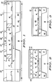
- FIG. 1 illustrates a cross-sectional view of an embodiment of a sensor 10.
- Sensor 10 is a semiconductor component that includes a substrate 11.
- Substrate 11 has a surface 19 opposite a surface 20 and is typically comprised of a semiconductor material such as, for example, silicon, a III-V compound semiconductor, or a II-VI compound semiconductor.
- FIG. 1 depicts portions of sensors 34 and 35 on substrate 11 and adjacent to sensor 10.
- FIG. 1 also portrays lines 36 and 37, which serve as scribe lines for singulating sensor 10 apart from sensors 34 and 35, respectively.
- Electrically insulating layer 32 is provided over surface 19 of substrate 11. Electrically insulating layer 32 is preferably a dielectric material such as, for example, silicon oxide or silicon nitride and can be deposited overlying substrate 11 using techniques known in the art.
- Substrate 11 has an optional recess 12 formed in a portion of surface 20 to facilitate heat dissipation in sensor 10 as described hereinafter.
- Recess 12 extends from surface 20 toward surface 19 and can expose a portion of electrically insulating layer 32.
- recess 12 is preferably etched into surface 20 using an anisotropic etchant that etches along specific crystal planes of substrate 11. The anisotropic etchant should not significantly etch electrically insulating layer 32 compared to substrate 11.
- anisotropic etchants that are suitable for use with single crystal silicon substrates include, but are not limited to, potassium hydroxide, ammonium hydroxide, cesium hydroxide, hydrazine, ethylenediamine/pyrocatechol, and tetramethylammonium hydroxide.
- Sensor 10 also includes a sensing element 14, which is supported by electrically insulating layer 32 and substrate 11 and which overlies recess 12.
- sensing element 14 is typically a resistor whose resistance changes upon exposure to a specific liquid or gas (not shown). At elevated operating temperatures, the resistivity of sensing element 14 is typically about 1 kiloohm - 50 megaohms.
- a control circuit (not shown) can detect a change in the resistivity of sensing element 14 by measuring a change in a current or voltage drop across sensing element 14.
- the control circuitry can be located on a different substrate or can be fabricated in substrate 11 to create an integrated chemical sensor system.
- Sensing element 14 is provided or formed over electrically insulating layer 32 and surface 19 of substrate 11 using techniques known in the art.
- sensing element 14 is comprised of an electrically conductive and chemically sensitive film including, but not limited to, metal oxides, transition metals, or noble metals.
- sensing element 14 can be comprised of tin oxide, zinc oxide, titanium oxide, or an alloy of platinum and gold. Different compositions of sensing element 14 permit the sensing or monitoring of different liquids or gases. It is understood that the material used for sensing element 14 can be doped to further improve the chemical sensitivity and selectivity of sensing element 14 and sensor 10.
- Sensing element 14 can be heated by an optional heating element 13 to help catalyze a chemical reaction between sensing element 14 and the desired liquid or gas.
- Heating element 13 is formed using techniques known to those skilled in the art.
- heating element 13 can be comprised of polysilicon or a metal such as platinum, gold, or the like.
- heating element 13 is located within electrically insulating layer 32, overlies recess 12, and underlies sensing element 14. It is understood that heating element 13 can be located on a different substrate than substrate 11. However, it is desirable for both heating element 13 and sensing element 14 to be located on substrate 11 for efficient heating and space conservation. Recess 12 in substrate 11 assists the heat dissipation or cooling of heating element 13 and sensor 10.
- Coupling lines 15 and 16 electrically couple features 17 and 18, respectively, to sensing element 14.
- Coupling lines 15 and 16 are comprised of an electrically conductive material such as, for example, a silicide or a metal.
- Coupling lines 15 and 16 are formed overlying electrically insulating layer 32 and surface 19 of substrate 11 using techniques known in the art.
- Features 17 and 18 provide electrical contacts for sensing element 14. For instance, assembly wire-bond wires can be coupled to features 17 and 18, which can serve as bonding pads.
- Features 17 and 18 are typically comprised of a metal including, but not limited to, gold or copper and are deposited overlying electrically insulating layer 32 and surface 19 of substrate 11 using sputtering, electroplating, chemical vapor deposition, or evaporation techniques.
- Adhesive 21 overlies coupling lines 15 and 16, overlies electrically insulating layer 32, overlies surface 19 of substrate 11, and is preferably spatially separated from sensing element 14 to avoid contaminating sensing element 14.
- Adhesive 21 can be any appropriate organic or inorganic bonding material such as, for example, a solder preform, a silk-screened epoxy, or fritted glass. If an electrically conductive adhesive is used for adhesive 21, an insulating layer (not shown) should electrically isolate coupling lines 15 and 16 from adhesive 21.
- Adhesive 21 couples or adheres electrically insulating layer 32 and a mesh, screen, or filter 22 in order to cap or package sensor 10.
- adhesive 21, electrically insulating layer 32, substrate 11, and filter 22 form a cavity 31.
- the volume of cavity 31 can be controlled by the thickness or height of adhesive 21.
- sensing element 14 is located inside cavity 31, and features 17 and 18 are located outside cavity 31.
- Filter 22 is provided over electrically insulating layer 32 and cavity 31 to filter, screen out, or prevent undesirable particles or chemicals from entering cavity 31.
- Filter 22 has a surface 23, an opposite surface 24, contact openings 25 and 30, and filtering holes 26, 27, 28, and 29 that serve as a filtering mechanism for filter 22 as discussed in more detail hereinafter.
- Filter 22 is preferably spatially separated from sensing element 14 to avoid contaminating or damaging sensing element 14.
- Filter 22 should have an appropriate thickness such that filter 22 is substantially rigid in order to prevent an elastic deformation of filter 22, in which filter 22 can contact and damage sensing element 14.
- filter 22 A wide variety of materials can be used for filter 22 as discussed hereinafter. However, many of the materials used for filter 22 may outgas a chemical at the elevated operating temperatures of sensor 10. Preferably, filter 22 is devoid of outgassing a chemical at the elevated operating temperatures to ensure an accurate chemical response of sensor 10 to the ambient. However, if filter 22 does outgas a chemical, filter 22 should not outgas a chemical that is capable of being detected by sensing element 14 in order to ensure accurate environmental monitoring for sensor 10. Similarly, adhesive 21, electrically insulating layer 32, substrate 11, coupling lines 15 and 16, and features 17 and 18 should also not outgas a chemical that can be sensed by sensing element 14 at the operating temperatures of sensor 10.
- Filter 22 can be comprised of a non-porous material or a porous or gas permeable material.
- non-porous materials include, but are not limited to, conventional single crystal silicon substrates, III-V compound semiconductor substrates, and II-VI compound semiconductor substrates.
- porous or gas permeable materials include, but are not limited to, porous silicon substrates, polymer membranes, porous ceramic, glass, charcoal filters, thermosets, alumina, polyimides, silica, and quartz.
- filter 22 When filter 22 is comprised of a porous or gas permeable material, filter 22 has an additional filtering mechanism that filter 22 does not have when comprised of a non-porous material. Certain liquids or gases can penetrate through certain porous or gas permeable materials and can enter cavity 31 without passing through filtering holes 26, 27, 28, or 29 of filter 22. Thus, a porous or gas permeable material can extend or enhance the filtering capabilities of filter 22 over that of a non-porous material in order to improve the chemical sensitivity and selectivity of sensor 10.
- Each porous or gas permeable material can have a different pore size that can be used to filter out different sizes of particles, chemicals, or molecules.
- the porous or gas permeable materials can be chemically active.
- a layer of a metallophthalocyanine polymer can be used for filter 22 in order to prevent nitrous oxide from passing into cavity 31.
- a compressed charcoal filter can be used for filter 22 to filter out and prevent hydrocarbons from entering cavity 31.
- a polyimide layer can be used for filter 22 to filter out and prevent moisture or water vapor from entering cavity 31.
- contact openings 25 and 30 are located over and permit access to features 17 and 18, respectively.
- contact openings 25 and 30 each have a dimension of approximately 50 - 1,000 microns to enable assembly wire-bond wires to extend through contact openings 25 and 30 to contact features 17 and 18, respectively.
- Contact openings 25 and 30 can also expose die singulation areas, identified as lines 36 and 37 in FIG. 1.
- Filtering holes 26, 27, 28, and 29 of filter 22 are located over cavity 31 and serve as a filtering mechanism for filter 22. While filter 22 can have a single hole overlying cavity 31, filter 22 preferably has a plurality of holes to permit adequate gas or liquid flow into and out of cavity 31 while maintaining adequate filtering functionality as described hereinafter. Filtering holes 26, 27, 28, and 29 each preferably have a diameter smaller than that of contact openings 25 and 30 to prevent unwanted particles from entering cavity 31. Thus, filter 22 protects sensing element 14 from physical damage and contamination during substrate dicing, other assembly processes, and operation of sensor 10.
- filtering holes 26, 27, 28, and 29 can each have a diameter on the order of angstroms to microns in order to prevent larger sized molecules or chemicals from entering cavity 31 and chemically reacting with sensing element 14.
- filter 22 is also used as a chemical filter - to improve the chemical selectivity and sensitivity of sensor 10.
- sensor 10 should only monitor small hydrocarbon molecules but that sensing element 14 chemically reacts with small hydrocarbon molecules, larger protein molecules, and even larger deoxyribonucleic acid molecules (DNA).
- filtering holes 26, 27, 28, and 29 each had a diameter on the order of a few angstroms, small hydrocarbon molecules can pass through filtering holes 26, 27, 28, and 29 to react with sensing element 14 while the larger protein molecules and the DNA molecules cannot pass through filtering holes 26, 27, 28, and 29 and cannot react with sensing element 14.
- the chemical selectivity of sensor 10 is improved.
- Filtering holes 26, 27, 28, and 29 and contact openings 25 and 30 are micromachined into filter 22 prior to coupling together filter 22 and substrate 11.
- Filtering holes 26, 27, 28, and 29 and contact openings 25 and 30 can be formed using a variety of different chemical and physical methods. For example, a reactive ion etch or a mechanical drilling technique can be used to form filtering holes 26, 27, 28, and 29 and contact openings 25 and 30 in filter 22.
- a reactive ion etch or a mechanical drilling technique can be used to form filtering holes 26, 27, 28, and 29 and contact openings 25 and 30 in filter 22.
- an anisotropic etchant similar to that used for recess 12 in substrate 11 can also be used to etch filtering holes 26, 27, 28, and 29 and contact openings 25 and 30.
- Filtering holes 26, 27, 28, and 29 and contact openings 25 and 30 can be etched from surface 23, from surface 24, or from both surfaces 23 and 24. As illustrated in FIG. 1, contact openings 25 and 30 and filtering hole 26 are etched from surface 23; hole 27 is etched from surface 24; and holes 28 and 29 are etched from surfaces 23 and 24. When holes are etched from both surfaces 23 and 24, a greater number or a higher density of holes can be provided in filter 22 compared to when the holes are only etched from a single surface of filter 22.
- FIG. 2 a partial cross-sectional view of an alternative embodiment of sensor 10 in FIG. 1 is portrayed as a sensor 40.
- Sensor 40 of FIG. 2 is similar to sensor 10 of FIG. 1, wherein the same reference numerals are used in FIGs. 1 and 2 to denote the same elements.
- a cavity 44 is formed by using adhesive 21 to couple together electrically insulating layer 32 and a filter 45. Cavity 44 and filter 45 are similar in purpose to cavity 31 and filter 22, respectively, of FIG. 1.
- Filter 45 is comprised of a layer 43 overlying a support layer 41.
- Support layer 41 is similar in composition to filter 22 of FIG. 1.
- Support layer 41 has a plurality of holes 42, which are covered by layer 43 and which are similar in purpose to filtering holes 26, 27, 28, and 29 of filter 22 in FIG. 1.
- Layer 43 is comprised of a porous or gas permeable material that serves as a selective filter to permit certain chemicals to pass through and to restrict the passage of other chemicals. Examples of porous materials and gas permeable materials suitable for layer 43 have previously been described herein.
- Layer 43 can be sputtered, sprayed, laminated, dispensed, or painted to a thickness of approximately 0.1 - 30 microns over support layer 41 after coupling support layer 41 to electrically insulating layer 32.
- layer 43 can be provided over support layer 41 before filter 45 is attached to electrically insulating layer 32.
- filter 45 can be coupled to electrically insulating layer 32 such that electrically insulating layer 32 and substrate 11 are located closer to layer 43 than support layer 41, which is a configuration that is not shown in FIG. 2.
- filter 45 is preferably coupled to electrically insulating layer 32 such that electrically insulating layer 32 and substrate 11 are located closer to support layer 41 than layer 43, as portrayed in FIG. 2, so that plurality of holes 42 will not become clogged during the operation of sensor 40.
- FIG. 3 a partial cross-sectional- view of another alternative embodiment of sensor 10 in FIG. 1 is depicted as a sensor 60.
- Sensor 60 of FIG. 3 is also similar to sensor 10 of FIG. 1, wherein the same reference numerals are used in FIGs. 1 and 3 to denote the same elements.
- adhesive 21 couples together electrically insulating layer 32 and a filter 61 to form a cavity 62 therebetween. Cavity 62 and filter 61 are similar in purpose to cavity 31 and filter 22, respectively, in FIG. 1.
- Filter 61 is comprised of a porous or gas permeable material that has an appropriate thickness to provide substantial rigidity in order to prevent damaging sensing element 14 as previously discussed herein. Unlike filter 22 of FIG. 1, filter 61 of FIG. 3 does not have any filtering holes. Filter 61 can be similar in composition to layer 43 of FIG. 2 and can have a thickness of approximately 50 - 500 microns.
- Sensors 10, 40, and 60 in FIGs. 1, 2, and 3, respectively, have several advantages over prior art sensors that are packaged in conventional metal T05 or T39 packages.
- cavities 31, 44, and 62 of FIGs. 1, 2, and 3, respectively, have smaller cavity volumes compared to the cavities or enclosed regions of the conventional metal T05 or T39 packages.
- sensors 10, 40, and 60 are smaller in size and more compact than the conventional metal T05 or T39 packages, which conserves space in any application.
- Sensors 10, 40, and 60 are at least approximately one hundred times smaller than the conventional metal T05 or T39 packages.
- cavities 31, 44 and 62 can be filled more quickly with a critical concentration of a chemical to be sensed by sensing element 14.
- a smaller cavity volume also permits faster purging of a critical chemical concentration.
- the response and refresh times for sensors 10, 40, and 60 are improved over the prior art.
- the cavity volumes of cavities 31, 44, and 62 can be controlled by the thickness or height of adhesive 21. The minimum cavity volume required for cavities 31, 44, and 62 is dependent upon the composition and operating temperatures of sensing element 14, the particular chemical being sensed, and the diffusion rate of an ambient gas or liquid into and out of cavities 31, 44, and 62.
- the manufacturing process for sensors 10, 40, and 60 is less time consuming, less expensive, and less labor intensive compared to the prior art.
- the fabrication of sensor 10 can be accomplished by using automated semiconductor wafer handling equipment, which reduces human intervention and improves manufacturing yields. In this manner, the fabrication of sensor 10 is compatible with high volume, production environments.
- sensors 10, 40, and 60 can be packaged or assembled using a wafer-level batch process, wherein hundreds or thousands of sensors are simultaneously packaged on a single semiconductor substrate before the individual sensors are singulated.
- This wafer-level batch packaging process improves throughput and is more cost effective than the manual and tedious prior art process of separately packaging one sensor at a time.
- the wafer-level packaging protects sensing element 14 from being damaged during die singulation because sensing element 14 is enclosed within cavity 31, 44, or 62 prior to the singulation process. Additionally, adhesive 21 and filters 22, 45, and 61 stiffen and strengthen sensors 10, 40, and 60, respectively, which lowers the potential for breakage. Accordingly, the manufacturing yields for sensors 10, 40, and 60 are further improved over the prior art.
Landscapes
- Chemical & Material Sciences (AREA)
- Chemical Kinetics & Catalysis (AREA)
- Electrochemistry (AREA)
- Physics & Mathematics (AREA)
- Health & Medical Sciences (AREA)
- Life Sciences & Earth Sciences (AREA)
- Analytical Chemistry (AREA)
- Biochemistry (AREA)
- General Health & Medical Sciences (AREA)
- General Physics & Mathematics (AREA)
- Immunology (AREA)
- Pathology (AREA)
- Investigating Or Analyzing Materials By The Use Of Fluid Adsorption Or Reactions (AREA)
Applications Claiming Priority (2)
| Application Number | Priority Date | Filing Date | Title |
|---|---|---|---|
| US08/620,729 US5798556A (en) | 1996-03-25 | 1996-03-25 | Sensor and method of fabrication |
| US620729 | 1996-03-25 |
Publications (3)
| Publication Number | Publication Date |
|---|---|
| EP0798554A2 true EP0798554A2 (de) | 1997-10-01 |
| EP0798554A3 EP0798554A3 (de) | 1997-10-15 |
| EP0798554B1 EP0798554B1 (de) | 2004-01-02 |
Family
ID=24487150
Family Applications (1)
| Application Number | Title | Priority Date | Filing Date |
|---|---|---|---|
| EP97104659A Expired - Lifetime EP0798554B1 (de) | 1996-03-25 | 1997-03-19 | Verfahren zur Herstellung eines Sensors |
Country Status (3)
| Country | Link |
|---|---|
| US (2) | US5798556A (de) |
| EP (1) | EP0798554B1 (de) |
| DE (1) | DE69727001T2 (de) |
Cited By (9)
| Publication number | Priority date | Publication date | Assignee | Title |
|---|---|---|---|---|
| WO1999057548A1 (de) * | 1998-04-30 | 1999-11-11 | Siemens Aktiengesellschaft | Wasserstoffsensor |
| WO2000062046A1 (de) * | 1999-04-14 | 2000-10-19 | Daimlerchrysler Ag | Dünnschicht-halbleiter-gassensor und verfahren zum nachweis von gasen |
| WO2001084132A3 (de) * | 2000-04-28 | 2002-08-01 | Vladimir Mirsky | Chemischer sensor und verfahren zur kalibrierung chemischer sensoren |
| WO2002048702A3 (de) * | 2000-12-15 | 2002-10-17 | Sensirion Ag | Stoffsensor mit schutzschicht |
| DE10245947A1 (de) * | 2002-09-30 | 2004-04-08 | Eads Deutschland Gmbh | Mikrogasanalysesystem mit beheizbarem Filter und Verfahren zur Gasanalyse |
| EP1936364A1 (de) * | 2006-12-20 | 2008-06-25 | AppliedSensor GmbH | Sensor und Herstellungsverfahren eines Sensors |
| CN104977326A (zh) * | 2014-04-07 | 2015-10-14 | 英诺晶片科技股份有限公司 | 传感器 |
| EP4105650A1 (de) * | 2021-06-15 | 2022-12-21 | MEAS France | Sensorvorrichtung mit deckschicht |
| SE2151590A1 (en) * | 2021-12-22 | 2023-06-23 | Senseair Ab | Capped semiconductor based sensor and method for its fabrication |
Families Citing this family (43)
| Publication number | Priority date | Publication date | Assignee | Title |
|---|---|---|---|---|
| JP4183789B2 (ja) * | 1998-01-14 | 2008-11-19 | 株式会社堀場製作所 | 物理現象および/または化学現象の検出装置 |
| US20040265838A1 (en) * | 1998-02-06 | 2004-12-30 | Affymetrix, Inc. | Method of manufacturing |
| JP2002502588A (ja) | 1998-02-06 | 2002-01-29 | アフィメトリックス インコーポレイテッド | 製造プロセスにおける品質管理の方法 |
| WO2000002014A1 (en) * | 1998-07-07 | 2000-01-13 | The Goodyear Tire And Rubber Company | Dual output capacitance interface circuit |
| TW396408B (en) * | 1998-11-20 | 2000-07-01 | Nat Science Council | Method of manufacturing ion sensor device and the device thereof |
| DE50011713D1 (de) * | 1999-12-08 | 2005-12-29 | Sensirion Ag Zuerich | Kapazitiver sensor |
| US6480370B1 (en) * | 1999-12-28 | 2002-11-12 | Intel Corporation | Polymeric dielectric material for high-energy density capacitors |
| DE10204458A1 (de) * | 2002-02-05 | 2003-08-14 | Stefan Raible | Gassensor |
| US7289230B2 (en) * | 2002-02-06 | 2007-10-30 | Cyberoptics Semiconductors, Inc. | Wireless substrate-like sensor |
| US20050224902A1 (en) * | 2002-02-06 | 2005-10-13 | Ramsey Craig C | Wireless substrate-like sensor |
| US6900508B2 (en) | 2002-04-16 | 2005-05-31 | Stmicroelectronics, Inc. | Embedded flat film molding |
| US9126165B1 (en) | 2002-04-24 | 2015-09-08 | The University Of North Carolina At Greensboro | Nucleic acid arrays to monitor water and other ecosystems |
| US8383342B2 (en) | 2002-04-24 | 2013-02-26 | The University Of North Carolina At Greensboro | Compositions, products, methods and systems to monitor water and other ecosystems |
| US8048623B1 (en) | 2002-04-24 | 2011-11-01 | The University Of North Carolina At Greensboro | Compositions, products, methods and systems to monitor water and other ecosystems |
| WO2005012716A1 (en) * | 2003-07-25 | 2005-02-10 | Siemens Vdo Automotive Inc. | Integrated vapor control valve and sensor |
| KR100529233B1 (ko) * | 2003-09-06 | 2006-02-24 | 한국전자통신연구원 | 센서 및 그 제조 방법 |
| US20050147489A1 (en) * | 2003-12-24 | 2005-07-07 | Tian-An Chen | Wafer supporting system for semiconductor wafers |
| DE112005000251B4 (de) * | 2004-01-27 | 2016-03-10 | H2Scan Corp. | Isolierte Gassensoranordnung |
| KR20070009600A (ko) * | 2004-03-09 | 2007-01-18 | 싸이버옵틱스 쎄미콘덕터 인코퍼레이티드 | 개선된 무선 기판형 센서 |
| US7424885B2 (en) * | 2005-02-24 | 2008-09-16 | Continental Automotive Canada, Inc. | Integrated vapor control valve with full range hydrocarbon sensor |
| DE102005016751B3 (de) * | 2005-04-11 | 2006-12-14 | Schott Ag | Verfahren zur Herstellung gehäuster elektronischer Bauelemente |
| US7893697B2 (en) | 2006-02-21 | 2011-02-22 | Cyberoptics Semiconductor, Inc. | Capacitive distance sensing in semiconductor processing tools |
| CN101410690B (zh) | 2006-02-21 | 2011-11-23 | 赛博光学半导体公司 | 半导体加工工具中的电容性距离感测 |
| KR100787228B1 (ko) * | 2006-06-12 | 2007-12-21 | 삼성전자주식회사 | 2축 지자기 센서 및 그 제작방법 |
| CN101517701B (zh) | 2006-09-29 | 2011-08-10 | 赛博光学半导体公司 | 衬底形的粒子传感器 |
| JP4739166B2 (ja) * | 2006-10-24 | 2011-08-03 | 本田技研工業株式会社 | ガスセンサ |
| EP2128573A1 (de) * | 2007-02-28 | 2009-12-02 | Yamatake Corporation | Sensor, sensortemperaturregelverfahren und abnormitätsbehebungsverfahren |
| CN101641576B (zh) * | 2007-02-28 | 2011-11-09 | 株式会社山武 | 流量传感器 |
| US7778793B2 (en) | 2007-03-12 | 2010-08-17 | Cyberoptics Semiconductor, Inc. | Wireless sensor for semiconductor processing systems |
| WO2009034843A1 (ja) * | 2007-09-11 | 2009-03-19 | The Ritsumeikan Trust | 半導体式ガスセンサ及びその製造方法 |
| KR100942439B1 (ko) * | 2007-12-28 | 2010-02-17 | 전자부품연구원 | 마이크로 가스센서 및 제조방법 |
| DE102010041763A1 (de) * | 2010-09-30 | 2012-04-05 | Siemens Aktiengesellschaft | Mikromechanisches Substrat |
| EP2565635B1 (de) | 2011-09-02 | 2017-11-15 | Sensirion AG | Sensorchip und Verfahren zur Herstellung eines Sensorchips |
| CN102730621B (zh) * | 2012-06-15 | 2015-05-27 | 西安交通大学 | 一种加热丝嵌入式硅基微热板及加工方法 |
| WO2013187910A1 (en) * | 2012-06-15 | 2013-12-19 | Empire Technology Development Llc | Self-cleaning lens |
| DE102013212735B4 (de) * | 2013-06-28 | 2021-07-22 | Robert Bosch Gmbh | Sensorbauteil für einen Gas- und/oder Flüssigkeitssensor, Herstellungsverfahren für ein Sensorbauteil für einen Gas- und/oder Flüssigkeitssensor und Verfahren zum Detektieren mindestens eines Stoffs in einem gasförmigen und/oder flüssigen Medium |
| US9461190B2 (en) * | 2013-09-24 | 2016-10-04 | Optiz, Inc. | Low profile sensor package with cooling feature and method of making same |
| DE102016112871A1 (de) * | 2015-07-31 | 2017-02-02 | Infineon Technologies Ag | Mikrofiltrationsvorrichtung |
| DE102017122043A1 (de) | 2017-09-22 | 2019-03-28 | Tdk Electronics Ag | MEMS-Gassensor |
| KR102437764B1 (ko) * | 2017-12-20 | 2022-08-30 | 삼성전자주식회사 | 센서 패키지, 센서 패키지의 제조 방법, 및 리드 구조체의 제조 방법 |
| DE102019201228B4 (de) * | 2019-01-31 | 2023-10-05 | Robert Bosch Gmbh | Verfahren zum Herstellen einer Mehrzahl von Sensoreinrichtungen und Sensoreinrichtung |
| DE102020203868B4 (de) * | 2020-03-25 | 2022-04-28 | Vitesco Technologies GmbH | Gassensor für ein Fahrzeug |
| TWI808541B (zh) * | 2021-11-22 | 2023-07-11 | 財團法人工業技術研究院 | 晶片封裝結構的透氣封裝蓋及其製造方法 |
Family Cites Families (17)
| Publication number | Priority date | Publication date | Assignee | Title |
|---|---|---|---|---|
| DE3029153A1 (de) * | 1980-07-31 | 1982-03-04 | Siemens AG, 1000 Berlin und 8000 München | Verfahren zur herstellung einer gaspermeablen polymermembran fuer analysengeraete und nach diesem verfahrrn hergestellte membram |
| US4472239A (en) * | 1981-10-09 | 1984-09-18 | Honeywell, Inc. | Method of making semiconductor device |
| JPS61178653A (ja) * | 1985-02-04 | 1986-08-11 | Matsushita Electric Works Ltd | ガス検知素子用フイルタの製法 |
| US4636767A (en) * | 1985-08-21 | 1987-01-13 | The United States Of America As Represented By The Secretary Of The Navy | Mixed semiconductor film device for monitoring gases |
| US4592824A (en) * | 1985-09-13 | 1986-06-03 | Centre Suisse D'electronique Et De Microtechnique S.A. | Miniature liquid junction reference electrode and an integrated solid state electrochemical sensor including the same |
| US4768070A (en) * | 1986-03-20 | 1988-08-30 | Hitachi, Ltd | Optoelectronics device |
| US4671852A (en) * | 1986-05-07 | 1987-06-09 | The Standard Oil Company | Method of forming suspended gate, chemically sensitive field-effect transistor |
| US4874500A (en) * | 1987-07-15 | 1989-10-17 | Sri International | Microelectrochemical sensor and sensor array |
| US4801380A (en) * | 1987-12-23 | 1989-01-31 | The Texas A&M University System | Method of producing a silicon film with micropores |
| GB8911607D0 (en) * | 1989-05-19 | 1989-07-05 | Emi Plc Thorn | A method of encapsulation for electronic devices and devices so encapsulated |
| US5204690A (en) * | 1991-07-01 | 1993-04-20 | Xerox Corporation | Ink jet printhead having intergral silicon filter |
| US5323051A (en) * | 1991-12-16 | 1994-06-21 | Motorola, Inc. | Semiconductor wafer level package |
| NL9401260A (nl) * | 1993-11-12 | 1995-06-01 | Cornelis Johannes Maria Van Ri | Membraan voor microfiltratie, ultrafiltratie, gasscheiding en katalyse, werkwijze ter vervaardiging van een dergelijk membraan, mal ter vervaardiging van een dergelijk membraan, alsmede diverse scheidingssystemen omvattende een dergelijk membraan. |
| JPH07140103A (ja) * | 1993-11-18 | 1995-06-02 | Seiko Epson Corp | 湿度センサ |
| DE4439286C2 (de) * | 1994-11-07 | 2003-07-31 | Gerhard Reis | Mehrlagiger und randseitig gelagerter Membrankörper für die elektrochemische Meßzelle und Verfahren zu dessen Herstellung |
| JPH0996622A (ja) * | 1995-09-29 | 1997-04-08 | Matsushita Electric Ind Co Ltd | ガスセンサおよびその製造方法 |
| US5963782A (en) * | 1997-08-01 | 1999-10-05 | Motorola, Inc. | Semiconductor component and method of manufacture |
-
1996
- 1996-03-25 US US08/620,729 patent/US5798556A/en not_active Expired - Lifetime
-
1997
- 1997-03-19 EP EP97104659A patent/EP0798554B1/de not_active Expired - Lifetime
- 1997-03-19 DE DE69727001T patent/DE69727001T2/de not_active Expired - Lifetime
-
1998
- 1998-05-29 US US09/086,740 patent/US6326228B1/en not_active Expired - Lifetime
Cited By (13)
| Publication number | Priority date | Publication date | Assignee | Title |
|---|---|---|---|---|
| WO1999057548A1 (de) * | 1998-04-30 | 1999-11-11 | Siemens Aktiengesellschaft | Wasserstoffsensor |
| US6513364B1 (en) | 1998-04-30 | 2003-02-04 | Siemens Aktiengesellschaft | Hydrogen sensor |
| WO2000062046A1 (de) * | 1999-04-14 | 2000-10-19 | Daimlerchrysler Ag | Dünnschicht-halbleiter-gassensor und verfahren zum nachweis von gasen |
| WO2001084132A3 (de) * | 2000-04-28 | 2002-08-01 | Vladimir Mirsky | Chemischer sensor und verfahren zur kalibrierung chemischer sensoren |
| WO2002048702A3 (de) * | 2000-12-15 | 2002-10-17 | Sensirion Ag | Stoffsensor mit schutzschicht |
| DE10245947B4 (de) * | 2002-09-30 | 2007-01-04 | Eads Deutschland Gmbh | Mikrogasanalysesystem mit beheizbarem Filter und Verfahren zur Gasanalyse |
| DE10245947A1 (de) * | 2002-09-30 | 2004-04-08 | Eads Deutschland Gmbh | Mikrogasanalysesystem mit beheizbarem Filter und Verfahren zur Gasanalyse |
| EP1936364A1 (de) * | 2006-12-20 | 2008-06-25 | AppliedSensor GmbH | Sensor und Herstellungsverfahren eines Sensors |
| CN104977326A (zh) * | 2014-04-07 | 2015-10-14 | 英诺晶片科技股份有限公司 | 传感器 |
| EP2930501A1 (de) * | 2014-04-07 | 2015-10-14 | Innochips Technology Co., Ltd. | Sensor |
| EP4105650A1 (de) * | 2021-06-15 | 2022-12-21 | MEAS France | Sensorvorrichtung mit deckschicht |
| SE2151590A1 (en) * | 2021-12-22 | 2023-06-23 | Senseair Ab | Capped semiconductor based sensor and method for its fabrication |
| SE545362C2 (en) * | 2021-12-22 | 2023-07-18 | Senseair Ab | Capped semiconductor based sensor and method for its fabrication |
Also Published As
| Publication number | Publication date |
|---|---|
| DE69727001T2 (de) | 2004-11-11 |
| EP0798554B1 (de) | 2004-01-02 |
| US5798556A (en) | 1998-08-25 |
| EP0798554A3 (de) | 1997-10-15 |
| DE69727001D1 (de) | 2004-02-05 |
| US6326228B1 (en) | 2001-12-04 |
Similar Documents
| Publication | Publication Date | Title |
|---|---|---|
| US6326228B1 (en) | Sensor and method of fabrication | |
| EP0856825B1 (de) | Herstellungsverfahren für integrierte Halbleitervorrichtung mit einem chemoresistiven Gasmikrosensor | |
| US5883009A (en) | Method of fabricating integrated semiconductor devices comprising a chemoresistive gas microsensor | |
| US4928513A (en) | Sensor | |
| EP0376721B1 (de) | Détecteur d'humidité | |
| JP3303146B2 (ja) | 半導体ウエハ・レベル・パッケージ | |
| US6114658A (en) | Device for the encapsulated reception of a material | |
| US6051854A (en) | Integrated semiconductor device comprising a chemoresistive gas microsensor and manufacturing process thereof | |
| US7713772B2 (en) | Micromechanical flow sensor with tensile coating | |
| KR100757695B1 (ko) | 부품 및 이의 제조 방법 | |
| WO2004105091A2 (en) | Sensor usable in ultra pure and highly corrosive environments | |
| JP2001326367A (ja) | センサおよびその製造方法 | |
| US7273763B1 (en) | Method of producing a micro-electromechanical element | |
| US20050012115A1 (en) | Ion sensitive field effect transistor and method for producing an ion sensitive field effect transistor | |
| CN105466463A (zh) | 传感器芯片 | |
| EP2759832B1 (de) | Elektrochemische Sensorvorrichtung | |
| EP1234326B1 (de) | Integriertes gehäuse für mikromechanische sensoren und dazugehörende kontrollschaltungen | |
| US6265750B1 (en) | Electrochemical gas sensor and method of making the same | |
| KR20050025383A (ko) | 센서 및 그 제조 방법 | |
| US7355200B2 (en) | Ion-sensitive field effect transistor and method for producing an ion-sensitive field effect transistor | |
| JP4271741B2 (ja) | 半導体部品 | |
| JP7105922B2 (ja) | 少なくとも1つの膜構成体の製造方法、マイクロメカニカルセンサ用の膜構成体、および部品 | |
| EP0211609A2 (de) | Auf chemische Stoffe empfindliche Halbleiterbauelemente und ihr Herstellungsverfahren | |
| JPH0196548A (ja) | センサ素子 | |
| US7703313B2 (en) | Conformal film micro-channels for a fluidic micro analyzer |
Legal Events
| Date | Code | Title | Description |
|---|---|---|---|
| PUAI | Public reference made under article 153(3) epc to a published international application that has entered the european phase |
Free format text: ORIGINAL CODE: 0009012 |
|
| PUAL | Search report despatched |
Free format text: ORIGINAL CODE: 0009013 |
|
| AK | Designated contracting states |
Kind code of ref document: A2 Designated state(s): DE FR GB |
|
| AK | Designated contracting states |
Kind code of ref document: A3 Designated state(s): DE FR GB |
|
| 17P | Request for examination filed |
Effective date: 19980415 |
|
| 17Q | First examination report despatched |
Effective date: 20000623 |
|
| RTI1 | Title (correction) |
Free format text: METHOD OF FABRICATING A SENSOR |
|
| RTI1 | Title (correction) |
Free format text: METHOD OF FABRICATING A SENSOR |
|
| GRAH | Despatch of communication of intention to grant a patent |
Free format text: ORIGINAL CODE: EPIDOS IGRA |
|
| GRAS | Grant fee paid |
Free format text: ORIGINAL CODE: EPIDOSNIGR3 |
|
| GRAA | (expected) grant |
Free format text: ORIGINAL CODE: 0009210 |
|
| AK | Designated contracting states |
Kind code of ref document: B1 Designated state(s): DE FR GB |
|
| REG | Reference to a national code |
Ref country code: GB Ref legal event code: FG4D |
|
| REF | Corresponds to: |
Ref document number: 69727001 Country of ref document: DE Date of ref document: 20040205 Kind code of ref document: P |
|
| ET | Fr: translation filed | ||
| PLBE | No opposition filed within time limit |
Free format text: ORIGINAL CODE: 0009261 |
|
| STAA | Information on the status of an ep patent application or granted ep patent |
Free format text: STATUS: NO OPPOSITION FILED WITHIN TIME LIMIT |
|
| 26N | No opposition filed |
Effective date: 20041005 |
|
| REG | Reference to a national code |
Ref country code: GB Ref legal event code: 732E |
|
| REG | Reference to a national code |
Ref country code: FR Ref legal event code: TP |
|
| PGFP | Annual fee paid to national office [announced via postgrant information from national office to epo] |
Ref country code: FR Payment date: 20140317 Year of fee payment: 18 |
|
| PGFP | Annual fee paid to national office [announced via postgrant information from national office to epo] |
Ref country code: GB Payment date: 20140327 Year of fee payment: 18 |
|
| PGFP | Annual fee paid to national office [announced via postgrant information from national office to epo] |
Ref country code: DE Payment date: 20140327 Year of fee payment: 18 |
|
| REG | Reference to a national code |
Ref country code: DE Ref legal event code: R119 Ref document number: 69727001 Country of ref document: DE |
|
| GBPC | Gb: european patent ceased through non-payment of renewal fee |
Effective date: 20150319 |
|
| REG | Reference to a national code |
Ref country code: FR Ref legal event code: ST Effective date: 20151130 |
|
| PG25 | Lapsed in a contracting state [announced via postgrant information from national office to epo] |
Ref country code: GB Free format text: LAPSE BECAUSE OF NON-PAYMENT OF DUE FEES Effective date: 20150319 Ref country code: DE Free format text: LAPSE BECAUSE OF NON-PAYMENT OF DUE FEES Effective date: 20151001 |
|
| PG25 | Lapsed in a contracting state [announced via postgrant information from national office to epo] |
Ref country code: FR Free format text: LAPSE BECAUSE OF NON-PAYMENT OF DUE FEES Effective date: 20150331 |