EP0793384B1 - Synchronermittlungs- und Demodulationsschaltung - Google Patents
Synchronermittlungs- und Demodulationsschaltung Download PDFInfo
- Publication number
- EP0793384B1 EP0793384B1 EP97301354A EP97301354A EP0793384B1 EP 0793384 B1 EP0793384 B1 EP 0793384B1 EP 97301354 A EP97301354 A EP 97301354A EP 97301354 A EP97301354 A EP 97301354A EP 0793384 B1 EP0793384 B1 EP 0793384B1
- Authority
- EP
- European Patent Office
- Prior art keywords
- circuit
- data
- synchronism
- bits
- parallel data
- Prior art date
- Legal status (The legal status is an assumption and is not a legal conclusion. Google has not performed a legal analysis and makes no representation as to the accuracy of the status listed.)
- Expired - Lifetime
Links
- 238000001514 detection method Methods 0.000 title claims description 141
- 238000006243 chemical reaction Methods 0.000 claims description 4
- 230000000694 effects Effects 0.000 claims description 2
- 230000001360 synchronised effect Effects 0.000 description 70
- 230000000717 retained effect Effects 0.000 description 43
- 238000000034 method Methods 0.000 description 26
- 230000001172 regenerating effect Effects 0.000 description 20
- 230000008569 process Effects 0.000 description 18
- 230000000873 masking effect Effects 0.000 description 16
- 230000001681 protective effect Effects 0.000 description 14
- 238000010586 diagram Methods 0.000 description 13
- 230000003111 delayed effect Effects 0.000 description 6
- 230000014509 gene expression Effects 0.000 description 4
- 230000008859 change Effects 0.000 description 3
- 230000001934 delay Effects 0.000 description 3
- 230000006870 function Effects 0.000 description 3
- 230000004044 response Effects 0.000 description 3
- 238000005070 sampling Methods 0.000 description 3
- 230000005236 sound signal Effects 0.000 description 3
- 229930091051 Arenine Natural products 0.000 description 1
- 230000001276 controlling effect Effects 0.000 description 1
- 230000008030 elimination Effects 0.000 description 1
- 238000003379 elimination reaction Methods 0.000 description 1
- 230000001788 irregular Effects 0.000 description 1
- 230000008707 rearrangement Effects 0.000 description 1
- 230000001105 regulatory effect Effects 0.000 description 1
- 238000007493 shaping process Methods 0.000 description 1
Images


Classifications
-
- H—ELECTRICITY
- H04—ELECTRIC COMMUNICATION TECHNIQUE
- H04N—PICTORIAL COMMUNICATION, e.g. TELEVISION
- H04N7/00—Television systems
- H04N7/24—Systems for the transmission of television signals using pulse code modulation
- H04N7/52—Systems for transmission of a pulse code modulated video signal with one or more other pulse code modulated signals, e.g. an audio signal or a synchronizing signal
- H04N7/54—Systems for transmission of a pulse code modulated video signal with one or more other pulse code modulated signals, e.g. an audio signal or a synchronizing signal the signals being synchronous
- H04N7/56—Synchronising systems therefor
-
- H—ELECTRICITY
- H04—ELECTRIC COMMUNICATION TECHNIQUE
- H04N—PICTORIAL COMMUNICATION, e.g. TELEVISION
- H04N5/00—Details of television systems
- H04N5/76—Television signal recording
- H04N5/91—Television signal processing therefor
- H04N5/93—Regeneration of the television signal or of selected parts thereof
- H04N5/935—Regeneration of digital synchronisation signals
-
- H—ELECTRICITY
- H04—ELECTRIC COMMUNICATION TECHNIQUE
- H04N—PICTORIAL COMMUNICATION, e.g. TELEVISION
- H04N5/00—Details of television systems
- H04N5/76—Television signal recording
- H04N5/91—Television signal processing therefor
- H04N5/92—Transformation of the television signal for recording, e.g. modulation, frequency changing; Inverse transformation for playback
- H04N5/9201—Transformation of the television signal for recording, e.g. modulation, frequency changing; Inverse transformation for playback involving the multiplexing of an additional signal and the video signal
- H04N5/9206—Transformation of the television signal for recording, e.g. modulation, frequency changing; Inverse transformation for playback involving the multiplexing of an additional signal and the video signal the additional signal being a character code signal
- H04N5/9208—Transformation of the television signal for recording, e.g. modulation, frequency changing; Inverse transformation for playback involving the multiplexing of an additional signal and the video signal the additional signal being a character code signal involving the use of subcodes
-
- H—ELECTRICITY
- H04—ELECTRIC COMMUNICATION TECHNIQUE
- H04N—PICTORIAL COMMUNICATION, e.g. TELEVISION
- H04N5/00—Details of television systems
- H04N5/76—Television signal recording
- H04N5/91—Television signal processing therefor
- H04N5/92—Transformation of the television signal for recording, e.g. modulation, frequency changing; Inverse transformation for playback
- H04N5/926—Transformation of the television signal for recording, e.g. modulation, frequency changing; Inverse transformation for playback by pulse code modulation
- H04N5/9261—Transformation of the television signal for recording, e.g. modulation, frequency changing; Inverse transformation for playback by pulse code modulation involving data reduction
Definitions
- the present invention relates to a synchronism detection and demodulating circuit for reproducing digital data which was divided into sync blocks and recorded in that format.
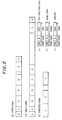
- Fig.1 shows the track pattern for digital video tape recorders based on the helical scanning technique.
- the track pattern is composed of four kinds of areas: ITI region where information such as a data format within the track, the absolute position on the track which the rotary head is scanning, etc., is recorded; AUDIO region where the audio signal is recorded; VIDEO region where the video signal is recorded; and SUBCODE region where extra-functional information is recorded, with gaps provided between the regions.
- AUDIO region i.e., AUDIO region, VIDEO region and SUBCODE region
- Figs.2(A), (B) and (C) show the sync block structures of AUDIO region, VIDEO region and SUBCODE region, respectively.
- two sync blocks and one sync block are provided at the beginning and end, respectively.
- These sync blocks are called pre-sync blocks for the two at the beginning and post-sync block for the one at the end.
- the pre-sync blocks facilitate the detection of the following sync blocks and the post-sync block indicates the end of the region.
- a, b and c designate different groups each having an identical block length and the same data format within the sync block.
- Fig.3 shows bit patterns of sync blocks.
- (1) shows a bit pattern before the 24/25 modulation and (2) a bit pattern after the 24/25 modulation.
- the ID which indicates the order of blocks and extra information for the data before modulation, ID parity for detecting or correcting an error in ID, and the audio signal, video signal, or extra-functional information (the audio signal, video signal and extra-functional information will be generically called 'recording information', hereinbelow), are subjected to a scrambling process for an MOD2 addition of an M-series random signal in order to enhance the random characteristic of the data. Then, in order to prevent the continuation of identical bits and control the d.c. component of the data, one bit is added to three words, or 24 bits.
- the aforementioned scrambling process is effected in the circuit shown in Fig.4, where a signal 401 with the extra bit added and a signal 402 which is generated by delaying the signal 401 after the 24/25 modulation by a span of two clock units, are subjected to the MOD2 addition to complete a pre-coding process.
- whether the extra bit is set at '1' or '0' is determined in accordance with the rule of the modulation for preventing the continuation of identical bits and controlling the d.c. component of the data.
- a sync pattern neither the scrambling process nor the pre-coding process is effected, but in order to prevent the continuation of identical bits and control the d.c. component of the data, one of two kinds of sync patterns of 17 bits, which have inverse allocations of bits '1' and '0', is selected to be added prior to the ID.
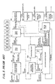
- FIG. 5 is a block diagram showing a conventional synchronism detection and demodulating circuit.
- a reference numeral 501 indicates a serial-to-parallel converter circuit which converts reproduced (hereinafter referred to as regenerative) data 512 inputted to a serial input into parallel data 514 of 5 bits and outputs the result whilst receiving a regenerative clock 513 and frequency divides it by 5 to output the result as a parallel clock 515.
- Designated at 502 is a delay circuit which delays parallel data 514 using shift registers based on parallel clock 515 so as to output delayed parallel data 516 and it also outputs tap data 517 from the mid tap of each register.
- a reference numeral 503 is a sync pattern detecting circuit, which detects sync patterns from tap data 517 and outputs a sync pattern detection pulse 518 which will become true when a sync pattern is detected while the aftermentioned window 528 is set to be true, and outputs a synchronous phase 519 indicating at which position the beginning of the sync pattern is located in the five bits of parallel data 514.
- a reference numeral 504 designates an ID detecting circuit, which detects the ID and ID parity of tap data 517 when the aftermentioned protective sync pattern detecting pulse 522 has become true, based on synchronous phase 519. This circuit then outputs the detected ID 521 and checks ID errors based on the detected ID and ID parity to output an ID error flag 520 which will become true when the ID contains errors.
- a reference numeral 505 designates a sync block protecting circuit which checks whether there is a sync block within parallel data 514, based on sync pattern detection pulse 518, ID 521, ID error flag 520, synchronous phase 519 and window 528 which is outputted from the window circuit 506 which will be explained later. If circuit 505 determines that there is a sync block, it outputs a synchronism establishment flag 527 which becomes true if a sync block has been found. After the flag became true, the sync pattern and ID are checked at the predictive position indicated by window 528 and then if errors occur N times (N is an integer equal to 1 or above) in a row, this flag 527 becomes false.
- Circuit 505 further outputs a sync block detection pulse 525 which indicates the beginning of the sync block, based on sync pattern detection pulse 518 when sync pattern detection pulse 518 has become true while window 528 is true, or by determining the beginning of the sync block based on window 528 even when the sync pattern detection pulse is false while window 528 is true and if synchronism establishment flag 527 is true.
- the circuit 505 also outputs a retained synchronous phase 524 which is held by sampling synchronous phase 519 at the moment when sync pattern detection pulse 518 becomes true while window 528 is true and outputs a protection ID 526 by correcting the ID, if it contains any error, based on the continuity of ID.
- a reference numeral 506 designates a window circuit which predicts which position the next sync pattern falls based on synchronism establishment flag 527, sync block detection pulse 525, protection ID 526 and retained synchronous phase 524 and outputs the predictive position and window 528 which becomes true only when the synchronism establishment flag stays false.
- Reference numerals 507 and 508 designate a barrel shifter and a rate converter circuit which, based on sync block detection pulse 525 and retained synchronous phase 524, delete extra bits in delayed parallel data 516 and output converted parallel data 529 made up of 8 bits which was converted from delayed parallel data 516 made up of 5 bits.
- This rate converter circuit 508 has memory capable of storing about 90 bytes (one sync).
- Designated at 509 is a descrambling circuit which, in order to undo the scrambling process which was performed at recording, carries out a descrambling process by which an MOD2 addition of the identical M-series random signal is performed at the same timing as that at the recording operation, thus outputting descrambled data 530.
- a reference numeral 510 designates a modified ID inserting circuit which inserts a protection ID 526 into a position at the beginning of descrambled data 530 to output demodulated data 531.
- Serial-to-parallel converter circuit 501 receives serial regenerative data 512, or x(0), x(1), x(2)..., in this order, and outputs parallel data 514, or X(0,4), X(5,9), X(10,14)..., in this order.
- X(0,4) represents the data from x(0) to x(4) arranged in parallel.
- Delay circuit 502 is composed of nine-step shift registers each made up of five bits. The first register is designated at T1, the second one is designated at T2, and in this way, the final register is designated at T9.
- regenerative data 512 is the data which was detected at partial response (1, 0, -1). Since the sync pattern is not pre-coded, the leading two bits within the 17 bits of the sync pattern can not take fixed values because they are affected by the two bits right before the sync pattern. Therefore, sync pattern detecting circuit 503 detects 15 bits from the rear end within 17 bits of the reproduced sync pattern as a sync pattern. From now on, the leading position of a sync pattern of 15 bits is referred to as the beginning of the sync pattern. Since regenerative data 512 inputted in serial is converted into 5 bit parallel data, regardless of the position in the sync pattern, there are five positions at which the beginning of the sync pattern can be located.
- sync pattern detecting circuit 503 receives as tap data, T9, T8, T7, each made up of 5 bits and the leading 4 bits of T6, in total, 19 bits (X(0, 18)).
- ID detecting circuit 504 receives as tap data, T6, T5, T4, T3 and T2, each made up of 5 bits and the leading 4 bits of T1, in total, 29 bits (X(15, 43)).
- Sync pattern detecting circuit 503 causes sync pattern detection pulse 518 to be true when the beginning of a sync pattern is detected from the output from T9, and determines synchronous phase 519 that indicates at which bit in T9 the beginning of the sync pattern is located. For example, when the beginning of the sync pattern is at X(0), synchronous phase 519 is set at '000'. When the beginning of the sync pattern is at X(4), synchronous phase 519 is set at '100' in order to indicate that the beginning of the sync pattern is in the final bit in T9.
- ID detecting circuit 504 detects the ID within tap data 517 and its ID parity based on sync pattern detection pulse 518 and synchronous phase 519. For example, if synchronous pattern detection pulse 518 is true and at the same time, synchronous phase 519 is '000', one byte in the front half of the ID (to be referred to as ID0, hereinbelow) is found to be X(15, 22), one byte in the rear half of the ID (to be referred to as ID1, hereinbelow) is to be X(24, 31), and the ID parity (to be referred to as IDP) is to be X(32, 39).
- ID detecting circuit 504 outputs the detected ID 521, and checks errors of the ID based on the ID parity to output ID error flag 520.
- sync block protecting circuit 505 judges that there is a sync block if window 528 and sync pattern detection pulse 518 are true and if ID error flag 520 is false, it causes sync block detection pulse 525 and synchronism establishment flag to be true and loads synchronous phase 519 to retain it as retained synchronous phase 524.
- the flag 527 will then be set to be false if the state in which at least any one of the following conditions 1, 2 and 3 is not satisfied has been detected N times in a row.
- the conditions to be checked are:
- sync pattern detection pulse 518 For synchronism protection, in the duration within which synchronism establishment flag 527 is true, if sync pattern detection pulse 518 does not become true while the window is true, the position of sync pattern detection pulse 518 is predicted based on window 528 so that sync block detection pulse 525 is caused to be true to retain the previous value of retained synchronous phase 524.
- ID protection even if sync pattern detection pulse 518 remains true or if ID error flag 520 at the predicted position of sync pattern detection pulse 518 is true, the current ID is predicted based on the past ID of the sync block so as to output protection ID 526.
- Window circuit 506 predicts the position of the next sync pattern based on sync block detection pulse 525 and protection ID 526 and outputs window 528.
- Barrel shifter 507 calculates the leading position of the synchronism based on retained synchronous phase, and rearranges the data so as to output the arranged data.
- Rate converter circuit 508 writes 24 bits other than extra bits in the lined-up data 532 into the memory. The data stored in the memory is read out per 8 bits based on a different clock to output converted parallel data 529.
- Descrambling circuit 509 performs the MOD2 addition of the converted parallel data 529 to the same M-series random signal at recording, outputting descrambled data 530.
- the modified ID is inserted into the beginning of descrambled data 530, producing demodulated data 531, which is sent to a code error correcting section 511.
- the present invention has been devised in order to attain the above object, and accordingly there is provided a synchronism detection and demodulating circuit for performing synchronism detection and demodulation of a reproduced data stream produced by a reproducing data which was recorded based on a modulating scheme whereby a digital data stream consisting of n-bit words is divided every m words and these are grouped as a unit, each group being supplemented by the addition of an extra 'p' bits ('p' is not an integer multiple of 'm'), to produce one block of ⁇ (n x m) + p ⁇ bits, comprising: a first circuit which converts the serially inputted reproduced data into parallel form using a clock signal obtained by irregularly frequency dividing a reproduction clock signal which is at the bit rate of the reproduced data, the frequency division producing m clock pulses at non-constant intervals for each successive group of ⁇ (n x m) + p ⁇ pulses of the reproduction clock, and the data conversion thereby producing redundancy in
- the first circuit may produce a first flag for use in deleting the redundancy part in the parallel data.
- the second circuit whilst detecting sync patterns, may delete redundancy in the parallel data, using said first flag obtained from the first circuit, and may produce a second flag for identifying the position of a sync pattern in the parallel data whilst taking into account the presence of the redundant part in the parallel data.
- the third circuit may delete the redundant part of the parallel data, using the first flag obtained from the first circuit, whilst detecting ID information in the parallel data using the second flag obtained from the second circuit.
- the fourth circuit may produce a third flag for indicating the positions of extra bits in the parallel data, whilst performing synchronism protection.
- the fifth circuit may rearrange the parallel data, based on a first flag generated in the first circuit for deleting the redundant part of the parallel data, a second flag generated in the second circuit for identifying the position of a sync pattern in the parallel data and a third flag generated in the fourth circuit for indicating positions of extra bits in the parallel data, whilst performing synchronism protection.
- 'n', 'm' and 'p' are set at 8, 3 and 1, respectively.
- the demodulating data which is obtained by the synchronism detection and demodulating process of the invention is given in the form of data lined up as word units, it is possible to subject the data to the code error correcting processing section without passing it through a rate converting circuit.
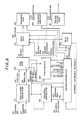
- a reference numeral 601 indicates a serial-to-parallel converter circuit which, based on the clock pulses from a regenerative clock 513, outputs a parallel clock 610 having a cycle of 25 clock units which are irregularly divided in 9 clock units, 8 clock units and 8 clock units. Circuit 601 also outputs parallel data 609 obtained by shaping regenerative data 512 into a parallel form with 9 bit width based on parallel clock 610. The circuit 601 further outputs a first flag in the form of parallel phase 614 providing phase information on the parallel clock containing the irregularity.
- Designated at 602 is a delay circuit which delays parallel data 609 using shift registers based on parallel clock 610 so as to output tap data 1 (612), tap data 2 (613) and tap data 3 (611) from respective output taps of the registers.
- a reference numeral 603 is a sync pattern detecting circuit, which detects sync patterns from tap data 1 (612) and outputs a sync pattern detection pulse 518 which will become true when a sync pattern is detected and outputs a second flag in the form of a synchronous phase 622 indicating in which position the beginning of the sync pattern is located in the nine bits of the parallel data.
- a reference numeral 604 designates an ID detecting circuit, which detects the ID and ID parity of tap data 2 (613) and outputs the detected ID 521 and checks ID errors based on the detected ID and ID parity to output an ID error flag 520 which will become true when the ID contains errors.
- a reference numeral 605 designates a sync block protecting circuit which checks whether there is a sync block within parallel data 609, and if circuit 605 determines that there is a sync block, it masks sync pattern detection pulse 518 which becomes true at an unexpected position, in order to prevent erroneous detection of a sync pattern. Further, circuit 605 outputs a protective sync pattern detection pulse 615 based on the position where sync pattern detection pulse 518 is predicted to become true even if sync pattern detection pulse 518 does not become true within the range where sync pattern detection pulse 518 is not true. Circuit 605 also outputs a retained synchronous phase 623 which is held by sampling synchronous phase 622 and a retained parallel phase 616 which is held by sampling parallel phase 614 only when sync pattern detection pulse 518 becomes true at the expected position.
- circuit 605 predicts the current ID based on the continuity of ID, using the previous ID which was detected when ID error flag 520 was false, and outputs the predicted ID as protection ID 526. Then, circuit 605 performs the following three checks: a first check, whether sync pattern detection pulse 518 is true at the predicted position; a second check, whether ID error flag 520 is false; and a third check, whether the detected ID matches the predicted ID.
- circuit 605 outputs a sync block detection pulse 525 and a third flag in the form of an intra-block phase 617 providing the information on the position where the extra bit is present within the sync block.
- a reference numeral 606 designates a window circuit that outputs three windows, namely, window 1 (619), window 2 (620) and window 3 (621), which become true at the time one clock unit before the predicted position where the next sync pattern detection pulse 518 will become true, at the predicted position, and at the time one clock unit after it, respectively.
- a reference numeral 607 designates a barrel shifter which deletes extra bits in tap data 3(611) and outputs lined-up data 618 of 8 bit words as units.
- Designated at 509 is a descrambling circuit which, in order to undo the scrambling process which was performed at recording, carries out a descrambling process, outputting descrambled data 530.
- a reference numeral 608 is a protection ID adding circuit which adds protection ID 526 at the beginning of descrambled data 530 to output demodulated data 531.
- a reference numeral 511 is a code error correcting circuit for correcting errors in demodulated data 531.
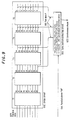
- Serial-to-parallel converter circuit 601 receives regenerative data 512 serially, inputting x(0), x(1), x(2).. in this order into its 9 bit shift register as shown in Fig.7.
- the serially inputted data is converted into 9 bit parallel load data 702 based on a load pulse signal 701 having a cycle of 25 clock units which are irregularly divided in 9 clock units, 8 clock units and 8 clock units of regenerative clock 513.
- the data is then latched by parallel clock 610 which is a clock generated by delaying load pulse signal 701 by one clock unit, and the latched data is outputted as parallel data 609, or X(0,8), X(8,16), X(16,24)..., in this order.
- X(0,8) represents the data from x(0) to x(8) arranged in parallel.
- the bit corresponding to x(0) is allotted to the leading bit, the bit corresponding to x(1) to the first bit, the bit corresponding to x(2) to the second bit, and similarly, the bit corresponding to x(7) to the seventh bit, and the bit corresponding to x(8) to the final bit.
- the bit corresponding to x(8) is allotted to the leading bit, and similarly, the bit corresponding to x(16) to the final bit.
- regenerative data 512 is made into the parallel arrangement of 9 bits in width based on load pulse signal 701 having a cycle of 25 clock units which are irregularly divided in 9 clock units, 8 clock units and 8 clock units of regenerative clock 513, 27 bits, i.e., for 3 clock units, of parallel data 609 contain two bits redundantly appearing in the data arranged in parallel.
- Parallel phase 614 is the signal indicating the positions of the data redundantly appearing in the parallel data.
- Parallel phase 614 is made up of two bits and like the parallel data 609 it is synchronized with parallel clock 610.
- parallel phase 614 is defined to be '10' for the period where parallel data 609 is X(0,8), '00' for the period where parallel data 609 is X(8,16), and '01' for the period where parallel data 609 is X(16,24).
- Delay circuit 602 is made up of five-steps of 9 bit shift registers.
- the first register is termed T1, the next register T2.
- the final register is termed T5.
- Fig.8 is a diagram showing the outputs from respective registers where parallel data 609 was shifted.
- the parallel data X(0,8) which was shifted and is outputted from register T1 is renamed as T1(0,8), for example.
- regenerative data 512 in this embodiment is the data which was detected at partial response (1,0,-1). Since the sync pattern is not pre-coded, the leading two bits within the 17 bits of the sync pattern can not take fixed values because they are affected by the two bits right before the sync pattern. Further, although two kinds of the sync patterns which have inverse allocations of bits were selectively recorded when recording was performed, the sync pattern of 15 bits other than the leading two bits contained in regenerative data 512 differs from the sync pattern at recording but is fixed at one kind of values. Accordingly, sync pattern detecting circuit 603 detects 15 bits other than leading two bits in the 17 bits of the reproduced sync pattern, as a sync pattern.
- the leading position of a sync pattern of 15 bits is referred to as the beginning of the sync pattern. Since regenerative data 512 inputted in serial is converted into 9 bits of parallel data, regardless of the position in the sync pattern, there are nine positions at which the beginning of the sync pattern can be located. The extra bit is located prior to the leading two bits at the beginning of each sync pattern of 15 bits and appears at the same position every three clock units in the parallel clock 610.
- Sync pattern detecting circuit 603 receives as tap data 1(612), 6 bits from the rear side of T5 , 9 bits each for T4 and T3, the leading one bit of T2, in total 25 bits, and deletes the redundant parallel data within tap data 1 using parallel phase 614.
- parallel phase 614 is set at '01' as shown in Fig.9, the final bit of T5 and the leading bit of T4 are redundant, the final bit of T4 and the leading bit of T3 also being redundant.
- parallel phase 614 is set at '10' as shown in Fig.10, the final bit of T5 and the leading bit of T4 are redundant, the final bit of T3 and the leading bit of T2 also being redundant.
- sync pattern detecting circuit 603 receives T5(3,8), T4(8,16), T3(16,24) and T2(25) as tap data 1(612). If the leading one of the redundant bits is deleted, tap data 1(612) will become T5(3,8), T4(9,,16), T3(17,24) and T2(25). This produces synchronism detection data 801 which will be represented by S(3,25).
- sync pattern detecting circuit 603 receives T5(11, 16), T4(16,24), T3(25,33) and T2(33) as tap data 1(612). After the leading one of the redundant bits is deleted, tap data 1(612) will become T5(11,16), T4(17,24), T3(25,33), thus producing synchronism detection data 801 represented by S(11,33).
- sync pattern detecting circuit 603 receives T5(19,24), T4(25,33), T3(33,41) and T2(41) as tap data 1(612). After the leading one of the redundant bits is deleted, tap data 1(612) will become T5(19,24), T4(25,33), T3(34,41), thus producing synchronism detection data 801 represented by S(19,41).
- synchronism detection data 801 will be formed into a row of data with a 23 bit width from serially inputted data.
- the leading one of the redundant bits was deleted, but the rear one of the redundant bits may alternatively be deleted. It is also possible to selectively delete either leading or rear one of the redundant bits, without any change of the function.
- Sync pattern detection pulse 518 will become true when the sync pattern of 15 bits is detected within synchronism detection data 801.
- the position of the sync pattern is determined as follows depending upon parallel phase 614.
- Synchronous phase 622 is a signal indicating the beginning of the sync pattern within synchronism detection data 801 and is represented in such a manner that when parallel phase 614 is '01' as shown in Fig.9 and the beginning of the sync pattern is located at the leading bit of synchronism detection data 801, specifically S(3,17), synchronous phase 622 is set at '0000', and when the beginning of the sync pattern is located at the second bit of synchronism detection data 801, or S(4,18), synchronous phase 622 is set at '0001'.
- the sync pattern detected when synchronism phase 622 is '1000' during the period where parallel phase 614 is '01' is also detected when synchronism phase 622 is '0000' during the period where parallel phase 614 is '10'. Also, the sync pattern detected when synchronism phase 622 is '1000' during the period where parallel phase 614 is '10', is also detected when synchronism phase 622 is '0000' during the period where parallel phase 614 is '00'.
- the operation is regulated so that the sync patterns which belong to '1000' will be detected only when parallel phase 614 is '00'. Specifically, the sync pattern residing at S(11,25) during the period where parallel phase 614 is '01' as well as the sync pattern residing at S(19,33) during the period where parallel phase 614 is '10' is neglected.
- sync pattern detecting circuit 603 can detect the sync pattern wherever the sync pattern is located within parallel data 609 and cause sync pattern detection pulse 518 to be true, without detecting the same sync pattern twice. Further, the configuration of outputting synchronous phase 622 can indicate at which bit the beginning of the sync pattern is located within parallel data 609.
- ID detecting circuit 604 receives as tap data 2(613), 8 bits from the rear side of T4, 9 bits each for T3, T2 and T1, in total 35 bits, and deletes the redundant parallel data within tap data 2 using parallel phase 614.
- parallel phase 614 is set at '10' as shown in Fig.10, the final bit of T3 and the leading bit of T2 are redundant, the final bit of T2 and the leading bit of T1 also being redundant.
- parallel phase 614 is set at '00' as shown in Fig.11, the final bit of T4 and the leading bit of T3 are redundant, the final bit of T3 and the leading bit of T2 also being redundant.
- ID detecting circuit 604 receives T4(17,24), T3(25,33), T2(33,41) and T1(41,49) as tap data 2(613). If the leading one of the redundant bits is deleted, tap data 2(613) will become T4(17,24), T3(25,33), T2(34,41) and T1(42,49), forming ID detection data 802, which will be represented by I(17,49).
- ID detecting circuit 604 receives T4(26,33), T3(33,41), T2(41,49) and T1(50,58) as tap data 2(613). After the leading one of the redundant bits is deleted, tap data 2(613) will become T4(26,33), T3(34,41), T2(42,49) and T1(50,58), thus producing ID detection data 802 represented by I(26,58).
- ID detecting circuit 604 receives T4(34,41), T3(41,49), T2(50,58) and T1(58,66) as tap data 2(613). After the leading one of the redundant bits is deleted, tap data 2(613) will become T4(34,41), T3(42,49), T2(50,58) and T1(59,66), thus producing ID detection data 802 represented by I(34,66).
- ID detection data 802 will be formed into a row of data with a 33 bit width from serially inputted data.
- the leading one of the redundant bits was deleted, but the rear one of the redundant bits may alternatively be deleted. It is also possible to selectively delete either leading or rear one of the redundant bits, without any change of the function.
- ID detecting circuit 604 based on retained synchronous phase 623, detects ID and ID parity contained in the ID detection data 802 which is obtained while protective sync pattern detection pulse 615 is true.
- protective sync pattern detection pulse 615 will become true one clock unit after the sync pattern detection pulse 518 does.
- the reason why protective sync pattern detection pulse 615 will become true one clock unit after the sync pattern detection pulse 518 does, will be explained later in the part concerning the operation of sync block protecting circuit 605.
- the ID and ID parity of the sync pattern which is detected during the period of Fig.9 will be detected from ID detection data I(17,49) of Fig.10; the ID and ID parity of the sync pattern which is detected during the period of Fig.10 will be detected from ID detection data I(26,58) of Fig.11; and the ID and ID parity of the sync pattern which is detected during the period of Fig.11 will be detected from ID detection data I(34,66) of Fig.12.
- the sync pattern which is detected during the period of Fig.9 has its beginning at a position between x(3) and x(10), and the beginning of it can be identified based on retained synchronous phase 623 such as x(3) when retained synchronous phase 623 is '0000', x(10) when retained synchronous phase 623 is '0111' and the like.
- the ID and ID parity corresponding to the sync pattern as shown in Fig.10 is detected from ID detection data I(17,49).
- IDO(0) can be determined as x(3+15), i.e., x(18).
- IDP(7) can be determined as x(3+39), i.e., x(42).
- IDO(0) can be determined as x(10+15), i.e., x(25).
- IDP(7) can be determined as x(10+39), i.e., x(49).
- the ID and ID parity corresponding to the sync pattern which is detected during the period of Fig.9 are all contained in ID detection data I(17,49) detected during the period of Fig.10 and can be detected therefrom.
- the sync pattern which is detected during the period of Fig.10 has its beginning at a position between x(11) and x(18), and the beginning of it can be identified similarly to the period of Fig.9, based on retained synchronous phase 623 such as x(11) when retained synchronous phase 623 is '0000', x(18) when retained synchronous phase 623 is '0111' and the like.
- IDO(0) can be determined as x(11+15), i.e., x(26).
- IDP(7) can be determined as x(11+39), i.e., x(50).
- IDO(0) can be determined as x(18+15), i.e., x(33).
- IDP(7) can be determined as x(18+39), i.e., x(57). Accordingly, the ID and ID parity corresponding to the sync pattern which is detected during the period of Fig.10 are all contained in I(26,58) of ID detection data 802 detected during the period of Fig.11 and can be detected therefrom.
- the sync pattern which is detected during the period of Fig.11 has its beginning at a position between x(19) and x(27), and the beginning of it can be identified similarly to the period of Fig.10, based on retained synchronous phase 623 such as x(19) when retained synchronous phase 623 is '0000', x(27) when retained synchronous phase 623 is '1000' and the like.
- IDO(0) can be determined as x(19+15), i.e., x(34).
- IDP(7) can be determined as x(19+39), i.e., x(58).
- IDO(0) can be determined as x(27+15), i.e., x(42).
- IDP(7) can be determined as x(27+39), i.e., x(66). Accordingly, the ID and ID parity corresponding to the sync pattern which is detected during the period of Fig.11 are all contained in ID detection data I(34,66) detected during the period of Fig.12 and can be detected therefrom.
- ID detecting circuit 604 can properly detect the ID and ID parity corresponding to a sync pattern wherever the sync pattern is located within parallel data 609, and checks errors based on the detected ID and ID parity so as to output ID error flag 520 which will become true when there is an error and output the detected ID 521.
- window circuit 606 determines the length of the sync block which is currently detected, based on the block number showing the order of the blocks within protection ID 526. Then, a value in accordance with the determined length of the sync block is loaded into a counter 1301 for predicting the position where the next sync pattern will be detected.
- window circuit 606 outputs three windows: a first window 1(619) which will become true when counter 1301 reaches the value corresponding to the position one clock unit before the predicted position where the next sync pattern detection pulse 518 will become true; a second window 2(620) which will become true when counter 1301 reaches the value corresponding to the predicted position where the next sync pattern detection pulse 518 will become true; and a third window 3(621) which will become true when counter 1301 reaches the value corresponding to the position one clock unit after the predicted position where the next sync pattern detection pulse 518 will become true.
- the data is judged to be a sync block only when the position, where sync pattern detection pulse 518 becomes true, does not deviate even one clock unit of regenerative clock 513 from the predicted position of the sync pattern which was determined based on the length of the previous sync block.
- the following two conditions are checked: a first condition that window 2(620) is true while sync pattern detection pulse 518 is true; and a second condition that synchronous phase 622 corresponds to retained synchronous phase 523. Only when these two conditions are satisfied, it is determined that a sync pattern was detected within the predicted range.
- the data is judged to be a sync block even when the position where sync pattern detection pulse 518 becomes true deviates one clock unit of regenerative clock 513 before or behind from the predicted position of the sync pattern which was determined based on the length of the pervious sync block.
- this condition there are cases in which it can be determined that a sync pattern was detected within the predicted range even when the first condition is not satisfied as long as retained synchronous phase 623 is '0000', '1000' or '0111', as will be explained below.
- sync pattern detection pulse 518 becomes true one clock unit of parallel clock 610 after, or during the period where window 3(621) is true.
- the window width is needed to be five clock units, for the combinations of retained parallel phase 616 and retained synchronous phase 623, it is determined that a sync pattern was detected when the data matched any one of the conditions in the five different columns on the same row, i.e., 2 clock units before, 1 clock unit before, the predicted position, 1 clock unit behind, and 2 clock units behind.
- window width it is possible to broaden the window width to 17 clocks by a similar manner as above. Moreover, when extra windows are added before window 1(619) or behind window 3(621), it is possible to broaden the window width further more.
- sync block protecting circuit 605 performs a NOR operation of masking sync pattern detection pulse 1302, 1 bit delayed pulse 1401 of the masking sync pattern detection pulse and 2 bit delayed pulse 1402 of the masking sync pattern detection pulse to produce a predictive synchronism masking signal 1403.
- Circuit 605 further performs an AND operation of predictive synchronism masking signal 1403 and window 3(621) to produce a predictive synchronism signal 1404.
- Circuit 605 then performs an OR operation of predictive synchronism signal 1404 and 1 clock unit delayed signal of masking sync pattern detection pulse 1302 to produce protective sync pattern detection pulse 615.
- sync pattern detection pulse 518 becomes true even if masking sync pattern detection pulse 1302 is not true in the synchronism protected state
- protective sync pattern detection pulse 615 that becomes true one clock after the predicted position is produced.
- predictive synchronism signal 1404 is masked so that protective sync pattern detection pulse 615 becomes true one clock unit after masking sync pattern detection pulse 1302 becomes true.
- sync block protecting circuit 605 retains ID 521 while protective sync pattern detection pulse 615 is true, to thereby generate a retained ID 1501, and retains ID 521 only when ID error flag 520 is false while protective sync pattern detection pulse 615 is true.
- circuit 605 produces a predicted ID 1502 which was predictive for the present ID on the basis of the ID 521 retained when ID error flag 520 was false, to thereby output an ID prediction error 1503 which will become true when retained ID 1501 and predictive ID 1502 do not coincide to each other.
- sync block protecting circuit 605 retains the inverse of a signal which is formed by delaying a masking sync pattern detection pulse 1302 by one clock unit to thereby produce a sync pattern error 1504.
- Circuit 605 also retains ID error flag 520 while protective sync pattern detection pulse 615 is true to thereby produce an ID parity error 1505. If ID prediction error 1503, sync pattern error 1504 and ID parity error 1505 are successively true, the situation of the errors are observed by counting the number of successions of the errors or checking other factors, to thereby set a synchronism ID error flag 1506 which determines whether the synchronism protected state should be maintained or not.
- Synchronism ID error flag 1506 will become true when the sync synchronism protected state should be disengaged. Based on this synchronism ID error flag 1506, synchronism establishment flag 527 is determined to be true or not. Only when synchronism establishment flag 527 is true, sync block detection pulse 525 which becomes true four clock units behind protective sync pattern detection pulse 615 is outputted.
- Sync block protecting circuit 605 outputs as protection ID 1501, retained ID 1501 when ID prediction error 1503 and ID parity error 1505 are both false, and otherwise outputs predictive ID 1502.
- Sync block protecting circuit 605 outputs a signal which indicates in which position the extra bit is present within tap data 3(611), namely intra-block phase 617 which is the output from a 3-cycle counter that is reset at 0 when the masking sync pattern detection pulse becomes true, and then counts up one by one and is reset when the count reaches 2.
- barrel shifter 607 deletes the extra bit and the redundant parallel data within tap data 3(611) on the basis of retained synchronous phase 623, retained parallel phase 616 and intra-block phase 617, rearranging the data to be lined up for each word as a unit.
- tap data 3(611) is made up of 9 bits of T5.
- synchronous phase 622 takes a value from '0000' to '0111' when masking sync pattern detection pulse 1302 becomes true, the extra bit resides within the tap data 3(611) at that moment.
- parallel phase 614 is '01' or '10'
- the extra bit redundantly parallel appears at the leading bit of the tap data 3(611) during the next clock period.
- synchronous phase 622 is '1000', the extra bit turns out to be present at the leading bit of the tap data 3(611) during the next clock period.
- intra-block phase 617 is a signal which is reset at 0 when masking sync pattern detection pulse 1302 becomes true and changes from 0 to 2 cyclically during the period of 3 clock units. Therefore, extra bits appear periodically every 3 clock units at the same bit position within tap data 3(611).
- Intra-block phase 617 is reset when masking sync pattern detection pulse 1302 becomes true.
- Extra bits appear periodically every 3 clock units at the same bit position within tap data 3(611).
- intra-block phase 617 the clock position where the extra bit appears corresponds to the position when masking sync pattern detection pulse 1302 is made true using intra-block phase 1607.
- the bit position of the extra bit within parallel data 609 will be determined using retained synchronous phase 623.
- retained synchronous phase 623 is '0000', it is indicated that the leading bit of synchronism detection data 801 resides at the beginning of the sync pattern, and it turns out that the beginning of the sync pattern resides at the third bit of parallel data 609.
- the extra bit Since the extra bit is known to be located two bits before the beginning of the sync pattern, the extra bit obviously resides at the first bit of parallel data 609.
- the leading bit of synchronism detection data 801 resides at the beginning of the sync pattern, and the beginning of the sync pattern is known to reside at the fourth bit of parallel data 609. Accordingly, the extra bit is obviously located at the second bit of parallel data 609.
- the redundant data arranged in parallel has the following features: parallel data 609 at the time when parallel phase 614 is '10', has redundant data arranged in parallel, at its final bit; parallel data 609 at the time when parallel phase 614 is '00', has redundant data arranged in parallel, at its leading and final bits; and parallel data 609 at the time when parallel phase 614 is '01', has redundant data arranged in parallel, at its leading bit.
- x(10) of T5 is selected to be deleted in this condition.
- parallel phase 614 is '10' and synchronous phase 622 takes a value from '0010' to '0111'
- x(11) to x(16) of T5 which exists two bits before the corresponding leading bit of synchronism, is selected to be deleted. In this way, 8 bits are selected from 9 bits of T5.
- 8 bit data which was obtained from T5 by deleting one bit using a selector 1 (1701) is one-latched in a latch circuit 1702 to produce 7 bits of data (the seventh bit is taken away from the output from selector 1).
- These 7 bits of data and the 8 bits of the direct output from selector 1 (1701) are inputted to a selector 2 (1703), where the leading bit of synchronism is determined with reference to synchronous phase 622 so that the order of the data is rearranged with the thus determined leading bit set at the beginning, to output them at intervals of 8 bits.
- This data forms lined-up data 618.
- Descrambling circuit 509 performs the MOD2 addition of lined-up data 618 to the same M-series random signal at recording, outputting descrambled data 530, which in turn is sent to protection ID adding circuit 608.
- the modified ID is inserted into the beginning of descrambled data 530 by protection ID adding circuit 608, thereby producing demodulated data 531, which is sent to code error correcting section 511.
- the circuit can be essentially operated based on a single kind of clock having a 8 bit cycle, it is possible to simplify the configuration of the clock circuit.
Landscapes
- Engineering & Computer Science (AREA)
- Multimedia (AREA)
- Signal Processing (AREA)
- Signal Processing For Digital Recording And Reproducing (AREA)
- Synchronisation In Digital Transmission Systems (AREA)
- Stabilization Of Oscillater, Synchronisation, Frequency Synthesizers (AREA)
Claims (7)
- Synchronermittlungs- und Demodulationsschaltung zur Synchronermittlung und Demodulation eines wiedergegebenen Datenstroms (512), welcher durch Wiedergabedaten erzeugt wurde, die ihrerseits auf der Grundlage eines Modulationsschemas aufgezeichnet wurden, wodurch ein digitaler Datenstrom, welcher aus n-Bitworten besteht, alle m Worte unterteilt und als Einheit gruppiert wird, wobei jede Gruppe durch Hinzufügen von zusätzlichen "p" Bits ("p" kein ganzzahliges Vielfaches von "m") ergänzt wird, um einen Block mit {(n x m) + p} Bits zu erzeugen, mit:einem ersten Schaltkreis (601, 602), welcher seriell eingegebene Wiedergabedaten in parallele Daten (609) umwandelt, und zwar unter Verwendung eines Taktsignals (610), welches durch eine irreguläre Frequenzunterteilung eines Wiedergabetaktsignals (513) erhalten wird, das seinerseits eine Bitrate der Wiedergabedaten (512) aufweist, wobei die Frequenzunterteilung m Taktpulse mit nicht-konstanten Abständen für jede nachfolgende Gruppe von {(n x m) + p} Pulsen des Wiedergabetakts erzeugt und wobei die Datenumwandlung dadurch eine Redundanz in den parallelen Daten erzeugt, und zwar in Form wiederholter Bits innerhalb jeder Gruppe von m parallelen Datenbereichen, welche durch die m unterteilten Taktpulse gespeichert oder verzögert sind;einem zweiten Schaltkreis (603), welcher Sync-Muster der parallelen Daten (609) aus dem ersten Schaltkreis (601) detektiert, während die Redundanz in den Paralleldaten gelöscht wird;einem dritten Schaltkreis (604), welcher eine ID-Information aus den Paralleldaten vom ersten Schaltkreis (601) ermittelt, während die Redundanz in den Paralleldaten gelöscht wird;einem vierten Schaltkreis (605), welcher einen Synchronismusschutz bewirkt, welcher das Vorsehen einer Synchronismusinformation (616, 623) aufrechterhält, selbst dann, wenn ein Sync-Muster trotz Vorhersage nicht ermittelt wurde, und zwar auf der Grundlage der Informationen des zweiten und dritten Schaltkreises, wobei die Synchronismusinformation die Anordnung des sync-Musters in den Paralleldaten anzeigt;einem fünften Schaltkreis (607), welcher die vom ersten Schaltkreis erhaltenen Paralleldaten neu anordnet, und zwar auf der Grundlage der Synchronismusinformation (616, 623) des vierten Schaltkreises, während die zusätzlichen Bits und der redundante Teil in den Paralleldaten (609) gelöscht werden.
- Synchronermittlungs- und Demodulationsschaltung nach Anspruch 1, bei welchem der erste Schaltkreis (601, 602) ein erstes Flag (614) zur Verwendung beim Löschen der Redundanz in den Paralleldaten erzeugt.
- Synchronermittlungs- und Demodulationsschaltung nach Anspruch 2, bei welchem der zweite Schaltkreis (603) während des Löschens der Sync-Muster die Redundanz in den Paralleldaten unter Verwendung des ersten Flags (614) des ersten Schaltkreises (601, 602) löscht und ein zweites Flag (622) zur Indentifizierung der Position eines Sync-Musters in den Paralleldaten erzeugt, während das Vorliegen des redundanten Teils in den Paralleldaten berücksichtigt wird.
- Synchronermittlungs- und Demodulationsschaltung nach Anspruch 3, bei welchem der dritte Schaltkreis (604) den redundanten Teil der Paralleldaten (609) löscht, und zwar unter Verwendung des ersten Flags des ersten Schaltkreises (601, 602), während die ID-Information in den Paralleldaten unter Verwendung des zweiten Flags des zweiten Schaltkreises detektiert wird
- Synchronermittlungs- und Demodulationsschaltung nach einem der vorangehenden Ansprüche, bei welchem der vierte Schaltkreis (605) ein drittes Flag (617) erzeugt, und zwar zum Anzeigen der Positionen der Zusatzbits in den Paralleldaten, und zwar während des Ausführens des Synchronismusschutzes.
- Synchronermittlungs- und Demodulationsschaltung nach Anspruch 1, bei welchem der fünfte Schaltkreis (607) die Paralleldaten neu anordnet, und zwar auf der Grundlage des ersten Flags, welches von dem ersten Schaltkreis (601, 602) erzeugt wurde, zum Löschen des redundanten Teils der Paralleldaten, auf der Grundlage eines zweiten Flags (622), welches vom zweiten Schaltkreis (603) erzeugt wurde, zum Identifizieren einer Position eines Sync-Musters in den Paralleldaten und auf der Grundlage eines dritten Flags (617), welches vom vierten Schaltkreis (605) erzeugt wurde, zum Anzeigen von Positionen von Zusatzbits in den Paralleldaten, während der Synchronismusschutz ausgeführt wird.
- Synchronermittlungs- und Demodulationsschaltung nach einem der vorangehenden Ansprüche, bei welchem "n", "m" und "p" auf 8, 3 bzw. 1 gesetzt werden.
Applications Claiming Priority (3)
| Application Number | Priority Date | Filing Date | Title |
|---|---|---|---|
| JP04271396A JP3441589B2 (ja) | 1996-02-29 | 1996-02-29 | 同期検出復調回路 |
| JP42713/96 | 1996-02-29 | ||
| JP4271396 | 1996-02-29 |
Publications (3)
| Publication Number | Publication Date |
|---|---|
| EP0793384A2 EP0793384A2 (de) | 1997-09-03 |
| EP0793384A3 EP0793384A3 (de) | 1999-02-10 |
| EP0793384B1 true EP0793384B1 (de) | 2001-06-06 |
Family
ID=12643719
Family Applications (1)
| Application Number | Title | Priority Date | Filing Date |
|---|---|---|---|
| EP97301354A Expired - Lifetime EP0793384B1 (de) | 1996-02-29 | 1997-02-28 | Synchronermittlungs- und Demodulationsschaltung |
Country Status (4)
| Country | Link |
|---|---|
| US (1) | US5963602A (de) |
| EP (1) | EP0793384B1 (de) |
| JP (1) | JP3441589B2 (de) |
| DE (1) | DE69705081T2 (de) |
Families Citing this family (11)
| Publication number | Priority date | Publication date | Assignee | Title |
|---|---|---|---|---|
| JP2970617B2 (ja) * | 1997-08-21 | 1999-11-02 | 日本電気株式会社 | フレーム同期回路 |
| DE19943739A1 (de) * | 1999-09-03 | 2001-05-10 | Infineon Technologies Ag | Vorrichtung und Verfahren zum Laufzeitausgleich |
| US6724848B1 (en) * | 2000-03-06 | 2004-04-20 | Intel Corporation | Sync regeneration in a universal serial bus |
| US7511098B2 (en) * | 2000-07-17 | 2009-03-31 | Valspar Sourcing, Inc. | Hardenable compositions comprising polyacid(s) and polyol(s) |
| JP4171171B2 (ja) * | 2000-10-25 | 2008-10-22 | 株式会社日立グローバルストレージテクノロジーズ | データ同期検出方法およびデータ同期検出装置、情報記録方法および情報記録装置、情報再生方法および情報再生装置、情報記録フォーマット、信号処理装置、情報記録再生装置、情報記録媒体 |
| US6934304B2 (en) * | 2001-01-24 | 2005-08-23 | Infineon Technologies, North America Corp. | T1/E1 framer array |
| JP3531626B2 (ja) * | 2001-07-09 | 2004-05-31 | ソニー株式会社 | データ伝送方法、ブロック同期信号検出方法及び再生装置 |
| US7284184B2 (en) * | 2003-01-30 | 2007-10-16 | International Business Machines Corporation | Forward error correction scheme compatible with the bit error spreading of a scrambler |
| US7496167B2 (en) * | 2005-01-20 | 2009-02-24 | Marvell World Trade Ltd. | Storage efficient sliding window sum |
| US8078898B2 (en) * | 2007-06-07 | 2011-12-13 | Texas Instruments Incorporated | Synchronizing TAP controllers with sequence on TMS lead |
| US8041981B2 (en) * | 2008-09-25 | 2011-10-18 | Apple Inc. | Synchronizing timing domains based on state variables |
Family Cites Families (15)
| Publication number | Priority date | Publication date | Assignee | Title |
|---|---|---|---|---|
| US4344180A (en) * | 1980-06-19 | 1982-08-10 | Bell Telephone Laboratories, Incorporated | Redundant word frame synchronization circuit |
| US4316284A (en) * | 1980-09-11 | 1982-02-16 | Bell Telephone Laboratories, Incorporated | Frame resynchronization circuit for digital receiver |
| JPS6057574A (ja) * | 1983-09-08 | 1985-04-03 | Sony Corp | 信号処理装置 |
| US4674088A (en) * | 1985-03-07 | 1987-06-16 | Northern Telecom Limited | Method and apparatus for detecting frame synchronization |
| NZ220548A (en) * | 1986-06-18 | 1990-05-28 | Fujitsu Ltd | Tdm frame synchronising circuit |
| KR0160279B1 (ko) * | 1988-12-20 | 1998-12-01 | 이우에 사또시 | 무선 통신 장치 |
| US5060239A (en) * | 1989-05-12 | 1991-10-22 | Alcatel Na Network Systems Corp. | Transfer strobe time delay selector and method for performing same |
| JPH0748725B2 (ja) * | 1990-07-25 | 1995-05-24 | 日本電気株式会社 | フレーム同期回路 |
| DE69122338T2 (de) * | 1990-08-03 | 1997-02-13 | Canon Kk | Synchronsignal-Detektorschaltung und dieselbe enthaltender Synchronsignal-Detektorapparat |
| GB2267799B (en) * | 1992-06-04 | 1995-11-08 | Sony Broadcast & Communication | Detection of synchronisation data |
| US5394410A (en) * | 1992-10-30 | 1995-02-28 | International Business Machines Corporation | Differentially coded and guard pulse position modulation for communication networks |
| DE69419055T2 (de) * | 1993-03-26 | 1999-12-23 | Sony Corp., Tokio/Tokyo | Vorrichtung zum Erzeugen eines Synchronisierungssignals |
| JP3500665B2 (ja) * | 1993-08-10 | 2004-02-23 | ソニー株式会社 | ディジタルビデオ信号記録装置及び再生装置 |
| KR950009690B1 (ko) * | 1993-09-14 | 1995-08-26 | 재단법인한국전자통신연구소 | 순환 여유검사(crc) 동기 장치 |
| KR0133423B1 (ko) * | 1994-12-09 | 1998-04-27 | 양승택 | 프레임 동기 장치(frame synchronizng device) |
-
1996
- 1996-02-29 JP JP04271396A patent/JP3441589B2/ja not_active Expired - Fee Related
-
1997
- 1997-02-03 US US08/795,318 patent/US5963602A/en not_active Expired - Fee Related
- 1997-02-28 EP EP97301354A patent/EP0793384B1/de not_active Expired - Lifetime
- 1997-02-28 DE DE69705081T patent/DE69705081T2/de not_active Expired - Fee Related
Also Published As
| Publication number | Publication date |
|---|---|
| EP0793384A3 (de) | 1999-02-10 |
| JP3441589B2 (ja) | 2003-09-02 |
| DE69705081T2 (de) | 2002-01-31 |
| DE69705081D1 (de) | 2001-07-12 |
| US5963602A (en) | 1999-10-05 |
| JPH09231692A (ja) | 1997-09-05 |
| EP0793384A2 (de) | 1997-09-03 |
Similar Documents
| Publication | Publication Date | Title |
|---|---|---|
| EP0673028B1 (de) | Aufzeichnungsmedium, Signalaufzeichnungsgerät dazu, und Signalwiedergabegerät dazu | |
| US4993029A (en) | Method and apparatus for randomizing data in a direct access storage device | |
| US4211997A (en) | Method and apparatus employing an improved format for recording and reproducing digital audio | |
| EP0074644B1 (de) | A PCM-Aufzeichnungs- und Wiedergabeanordnung mit einem datenfehlerfreien Format | |
| EP0793384B1 (de) | Synchronermittlungs- und Demodulationsschaltung | |
| EP0710956B1 (de) | Wiedergabegerät für Informationssignale und Verfahren zur Wiedergabe von Informationssignalen | |
| US4356564A (en) | Digital signal transmission system with encoding and decoding sections for correcting errors by parity signals transmitted with digital information signals | |
| CA1099023A (en) | Method and system for transmitting and receiving interleaved blocks of encoded data words to minimize error distortion in the recovery of said data words | |
| GB1599156A (en) | Recording digital signals | |
| JPH06195893A (ja) | データ記録方法及び装置 | |
| CA1260145A (en) | Synchronizing signal decoding | |
| KR100239624B1 (ko) | 비데오신호.오디오신호기록장치 | |
| US5021897A (en) | Memory system for recording and reproducing block unit data | |
| EP0504849B1 (de) | PCM-Signal Aufzeichnungssystem | |
| EP0418885A2 (de) | Gerät zur Übertragung von digitalen Daten | |
| US4442520A (en) | Signal error detecting | |
| US5228041A (en) | Sync signal detection system in a memory system for recording and reproducing block unit data | |
| JP2947081B2 (ja) | デジタル情報変調装置 | |
| JP2883554B2 (ja) | データエンコード方法、データ再生方法、データ形成装置及びデータ再生装置 | |
| JP3240869B2 (ja) | 同期回路 | |
| KR100223160B1 (ko) | 디지탈-브이씨알(d-vcr)의 동기신호 기록.검출방법 및 그 장치 | |
| JP3868047B2 (ja) | バッファ回路 | |
| JP3321884B2 (ja) | 同期ブロック検出方法および同期ブロック検出装置 | |
| JP2637089B2 (ja) | デイジタルvtrの信号処理方式 | |
| KR0145261B1 (ko) | 디지틀신호기록장치 |
Legal Events
| Date | Code | Title | Description |
|---|---|---|---|
| PUAI | Public reference made under article 153(3) epc to a published international application that has entered the european phase |
Free format text: ORIGINAL CODE: 0009012 |
|
| AK | Designated contracting states |
Kind code of ref document: A2 Designated state(s): DE GB |
|
| PUAL | Search report despatched |
Free format text: ORIGINAL CODE: 0009013 |
|
| AK | Designated contracting states |
Kind code of ref document: A3 Designated state(s): DE GB |
|
| 17P | Request for examination filed |
Effective date: 19990420 |
|
| 17Q | First examination report despatched |
Effective date: 19990521 |
|
| GRAG | Despatch of communication of intention to grant |
Free format text: ORIGINAL CODE: EPIDOS AGRA |
|
| GRAG | Despatch of communication of intention to grant |
Free format text: ORIGINAL CODE: EPIDOS AGRA |
|
| GRAH | Despatch of communication of intention to grant a patent |
Free format text: ORIGINAL CODE: EPIDOS IGRA |
|
| GRAH | Despatch of communication of intention to grant a patent |
Free format text: ORIGINAL CODE: EPIDOS IGRA |
|
| GRAA | (expected) grant |
Free format text: ORIGINAL CODE: 0009210 |
|
| AK | Designated contracting states |
Kind code of ref document: B1 Designated state(s): DE GB |
|
| REF | Corresponds to: |
Ref document number: 69705081 Country of ref document: DE Date of ref document: 20010712 |
|
| REG | Reference to a national code |
Ref country code: GB Ref legal event code: IF02 |
|
| PLBE | No opposition filed within time limit |
Free format text: ORIGINAL CODE: 0009261 |
|
| STAA | Information on the status of an ep patent application or granted ep patent |
Free format text: STATUS: NO OPPOSITION FILED WITHIN TIME LIMIT |
|
| 26N | No opposition filed | ||
| PGFP | Annual fee paid to national office [announced via postgrant information from national office to epo] |
Ref country code: DE Payment date: 20070222 Year of fee payment: 11 |
|
| PGFP | Annual fee paid to national office [announced via postgrant information from national office to epo] |
Ref country code: GB Payment date: 20070228 Year of fee payment: 11 |
|
| GBPC | Gb: european patent ceased through non-payment of renewal fee |
Effective date: 20080228 |
|
| PG25 | Lapsed in a contracting state [announced via postgrant information from national office to epo] |
Ref country code: DE Free format text: LAPSE BECAUSE OF NON-PAYMENT OF DUE FEES Effective date: 20080902 |
|
| PG25 | Lapsed in a contracting state [announced via postgrant information from national office to epo] |
Ref country code: GB Free format text: LAPSE BECAUSE OF NON-PAYMENT OF DUE FEES Effective date: 20080228 |