EP0793293B1 - Antenneneinheit - Google Patents
Antenneneinheit Download PDFInfo
- Publication number
- EP0793293B1 EP0793293B1 EP97102904A EP97102904A EP0793293B1 EP 0793293 B1 EP0793293 B1 EP 0793293B1 EP 97102904 A EP97102904 A EP 97102904A EP 97102904 A EP97102904 A EP 97102904A EP 0793293 B1 EP0793293 B1 EP 0793293B1
- Authority
- EP
- European Patent Office
- Prior art keywords
- antenna unit
- substrate
- power supply
- electronic device
- conductor
- Prior art date
- Legal status (The legal status is an assumption and is not a legal conclusion. Google has not performed a legal analysis and makes no representation as to the accuracy of the status listed.)
- Expired - Lifetime
Links
- 239000004020 conductor Substances 0.000 claims description 72
- 230000005855 radiation Effects 0.000 claims description 39
- 239000000758 substrate Substances 0.000 claims description 28
- 230000005540 biological transmission Effects 0.000 claims description 9
- 239000003989 dielectric material Substances 0.000 claims description 8
- 239000000696 magnetic material Substances 0.000 claims description 6
- XEEYBQQBJWHFJM-UHFFFAOYSA-N Iron Chemical compound [Fe] XEEYBQQBJWHFJM-UHFFFAOYSA-N 0.000 claims description 4
- PXHVJJICTQNCMI-UHFFFAOYSA-N Nickel Chemical compound [Ni] PXHVJJICTQNCMI-UHFFFAOYSA-N 0.000 claims description 4
- VYPSYNLAJGMNEJ-UHFFFAOYSA-N Silicium dioxide Chemical compound O=[Si]=O VYPSYNLAJGMNEJ-UHFFFAOYSA-N 0.000 claims description 4
- QVQLCTNNEUAWMS-UHFFFAOYSA-N barium oxide Chemical compound [Ba]=O QVQLCTNNEUAWMS-UHFFFAOYSA-N 0.000 claims description 4
- PLDDOISOJJCEMH-UHFFFAOYSA-N neodymium(3+);oxygen(2-) Chemical compound [O-2].[O-2].[O-2].[Nd+3].[Nd+3] PLDDOISOJJCEMH-UHFFFAOYSA-N 0.000 claims description 4
- GWEVSGVZZGPLCZ-UHFFFAOYSA-N Titan oxide Chemical compound O=[Ti]=O GWEVSGVZZGPLCZ-UHFFFAOYSA-N 0.000 claims description 2
- 229910017052 cobalt Inorganic materials 0.000 claims description 2
- 239000010941 cobalt Substances 0.000 claims description 2
- GUTLYIVDDKVIGB-UHFFFAOYSA-N cobalt atom Chemical compound [Co] GUTLYIVDDKVIGB-UHFFFAOYSA-N 0.000 claims description 2
- 239000011888 foil Substances 0.000 claims description 2
- 229910052742 iron Inorganic materials 0.000 claims description 2
- 229910052759 nickel Inorganic materials 0.000 claims description 2
- TWNQGVIAIRXVLR-UHFFFAOYSA-N oxo(oxoalumanyloxy)alumane Chemical compound O=[Al]O[Al]=O TWNQGVIAIRXVLR-UHFFFAOYSA-N 0.000 claims description 2
- 239000000377 silicon dioxide Substances 0.000 claims description 2
- OGIDPMRJRNCKJF-UHFFFAOYSA-N titanium oxide Inorganic materials [Ti]=O OGIDPMRJRNCKJF-UHFFFAOYSA-N 0.000 claims description 2
- 230000004048 modification Effects 0.000 description 12
- 238000012986 modification Methods 0.000 description 12
- 238000004804 winding Methods 0.000 description 6
- 230000008878 coupling Effects 0.000 description 5
- 238000010168 coupling process Methods 0.000 description 5
- 238000005859 coupling reaction Methods 0.000 description 5
- 239000012212 insulator Substances 0.000 description 5
- 239000004615 ingredient Substances 0.000 description 3
- 239000000463 material Substances 0.000 description 3
- RYGMFSIKBFXOCR-UHFFFAOYSA-N Copper Chemical compound [Cu] RYGMFSIKBFXOCR-UHFFFAOYSA-N 0.000 description 1
- 229910000881 Cu alloy Inorganic materials 0.000 description 1
- 229910001252 Pd alloy Inorganic materials 0.000 description 1
- 229910052782 aluminium Inorganic materials 0.000 description 1
- XAGFODPZIPBFFR-UHFFFAOYSA-N aluminium Chemical compound [Al] XAGFODPZIPBFFR-UHFFFAOYSA-N 0.000 description 1
- PNEYBMLMFCGWSK-UHFFFAOYSA-N aluminium oxide Inorganic materials [O-2].[O-2].[O-2].[Al+3].[Al+3] PNEYBMLMFCGWSK-UHFFFAOYSA-N 0.000 description 1
- 238000006243 chemical reaction Methods 0.000 description 1
- 229910052802 copper Inorganic materials 0.000 description 1
- 239000010949 copper Substances 0.000 description 1
- 238000010586 diagram Methods 0.000 description 1
- 238000010304 firing Methods 0.000 description 1
- 239000011810 insulating material Substances 0.000 description 1
- 238000010030 laminating Methods 0.000 description 1
- 239000006247 magnetic powder Substances 0.000 description 1
- 238000010295 mobile communication Methods 0.000 description 1
- SWELZOZIOHGSPA-UHFFFAOYSA-N palladium silver Chemical compound [Pd].[Ag] SWELZOZIOHGSPA-UHFFFAOYSA-N 0.000 description 1
- 230000035699 permeability Effects 0.000 description 1
- 238000007747 plating Methods 0.000 description 1
- 239000000843 powder Substances 0.000 description 1
- 238000007639 printing Methods 0.000 description 1
- 239000004065 semiconductor Substances 0.000 description 1
- 229910052709 silver Inorganic materials 0.000 description 1
- 239000004332 silver Substances 0.000 description 1
- 238000007740 vapor deposition Methods 0.000 description 1
Images


Classifications
-
- H—ELECTRICITY
- H01—ELECTRIC ELEMENTS
- H01Q—ANTENNAS, i.e. RADIO AERIALS
- H01Q23/00—Antennas with active circuits or circuit elements integrated within them or attached to them
-
- H—ELECTRICITY
- H01—ELECTRIC ELEMENTS
- H01Q—ANTENNAS, i.e. RADIO AERIALS
- H01Q1/00—Details of, or arrangements associated with, antennas
- H01Q1/36—Structural form of radiating elements, e.g. cone, spiral, umbrella; Particular materials used therewith
- H01Q1/38—Structural form of radiating elements, e.g. cone, spiral, umbrella; Particular materials used therewith formed by a conductive layer on an insulating support
-
- H—ELECTRICITY
- H01—ELECTRIC ELEMENTS
- H01Q—ANTENNAS, i.e. RADIO AERIALS
- H01Q9/00—Electrically-short antennas having dimensions not more than twice the operating wavelength and consisting of conductive active radiating elements
- H01Q9/04—Resonant antennas
- H01Q9/0407—Substantially flat resonant element parallel to ground plane, e.g. patch antenna
Definitions
- the present invention generally relates to an antenna unit and, more particularly, to an antenna unit for use in a mobile communication system and in a local area network (LAN).
- LAN local area network
- Fig. 10 is a side view of a conventional tip antenna.
- the tip antenna 50 consists of: a rectangular-prism-like insulator 51 formed by stacking up insulating layers (not shown) made of powdery insulating materials such as alumina and steatite; a conductor 52 which is made of silver or silver-palladium alloy or the like and is formed like a coil in the insulator 51; a magnetic element 53 which is made of magnetic powder such as ferric powder and is formed inside the insulator 51 and the coil-like conductor 52; external connecting terminals 54a and 54b which are made to adhere and are baked in such a manner as to stick to the lead-out end (not shown) of the conductor 52 after the firing of the insulator 51.
- the tip antenna 50 is configured so that the coil-like conductor 52 is wound around the magnetic element 53 and a space therearound is filled with the insulator 51. Further, by using a material having a low relative permeability as the magnetic element 53, a tip antenna 50 which has a low resonance frequency of tens to hundreds MHz can be produced.
- a similar antenna in e.g. disclosed in JP-A-59017705.
- the aforementioned conventional tip antenna has a problem in that when produced as a small-sized antenna having a low resonance frequency, the gain and bandwidth thereof are degraded.
- EP 0 473 981 A discloses an integrated circuit card for a data processing device having a patch antenna provided on a surface of the card and which is connected by microstrip lines for impedance conversion to respective antenna receiving and transmitting circuits.
- US-A-5,386,214 relates to an electronic circuit device having a printed circuit board on which a circuit pattern is formed and on which components are mounted. On a second surface a coupling stub is formed which is connected to the circuit pattern and a plane antenna having an antenna element formed on a first surface of a dielectric substrate is placed on the second surface of the printed circuit board.
- US-A-5,185,613 discloses a hybrid structure having a lens, an antenna array and a semiconductor microcircuit wherein the antenna array is formed on a surface of the lens or on a surface of the substrate and wherein the respective antennas are in turn connected by bump bonds to the microcircuit.
- US-A-4,888,597 discloses a millimeter and submillimeter wave antenna wherein the antenna structure includes a horn disposed on a substrate for focussing electromagnetic energy with respect to an antenna.
- the present invention provides an antenna unit comprising an antenna body having a substrate, the substrate having a first main surface and a mounting surface parallel to the first main surface, and a side surface connecting the first main surface and the mounting surface, the substrate comprising at least one of a dielectric material and a magnetic material; at least one power supply conductor having a power supply end and a free end; at least one power supply terminal for applying a voltage to the power supply end of the power supply conductor; and a power radiation conductor electrically insulated from and electromagentically coupled to the power supply conductor, the power radiation conductor arranged at the first main surface; wherein the at least one power supply conductor is spirally wound and arranged inside the substrate, the spirally wound conductor having a spiral axis extending parallel to the mounting surface; the at least one power supply terminal is arranged on the side surface of the substrate of the antenna body.
- the antenna unit according to the present invention is provided with a power supply conductor and a power radiation conductor. Therefore, the power radiation conductor can be operated as a radiating plate (namely, a radiator). Moreover, the power supply conductor can be operated as an exciter.
- the power radiation conductor operates as a radiating plate, while the power supply conductor operates as an exciter.
- the power radiation conductor operates as a radiating plate
- the power supply conductor operates as an exciter.
- Fig.1 is a perspective view of an antenna unit according to the present invention.
- a power supply conductor 22 is wound such that the winding axis C of the power supply conductor 22 of the antenna body 21 is parallel to a mounting surface 231, namely, the power supply conductor 22 is wound in a spiral in the longitudinal direction of a substrate 23.
- the antenna unit 20 has a spiral power supply conductor 22 and further has a nearly rectangular power radiation conductor 12. Further, there is provided electromagnetic coupling between the power supply conductor 22 and the power radiation conductor 12. Thus, there is generated a capacitance between the power radiation conductor 12 and a ground electrode (not shown). Consequently, the antenna unit 20 becomes an antenna, which has a low resonance frequency.
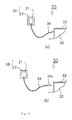
- Fig. 2 and Fig. 3 are, respectively, a top view and a sectional view of an electronic device on which the antenna unit 20 is mounted.
- the antenna unit 20 is mounted on a printed circuit board 32 on which electronic parts composing an RF control portion 31 of an electronic device 30 are mounted.
- the antenna unit 20 is connected to the RF control portion 30 through a transmission line (not shown) or the like.
- the printed circuit board 32 on which the antenna unit 20 is mounted, is placed in a casing 33 of the electronic device 30.
- the power radiation conductor 12 of the antenna unit 20 may be in contact with the casing 33 thereof but need not be in contact therewith.
- Fig. 4 is a sectional view of a modification of the electronic device in a case that the antenna unit 20 is mounted thereon.
- the casing 33 of the electronic device 30 comprises a carrying case 33a and a cover or lid 33b reclosably connected to the carrying case 33a.
- the printed circuit board 32, on which the RF control portion 31 of the electronic device 30 is mounted is provided in the carrying case 33a.
- the antenna unit 20 is provided on the back surface of the cover 33b. The antenna unit 20 is connected to the RF control portion 31 of the electronic device 30 through a cable (not shown) or the like.
- the antenna unit 20 can be disposed in an orientation in which radiation reception/transmission is optimum.
- Fig. 4 illustrates the usage conditions of the electronic device.
- the electronic device is carried in a state in which the cover 33b is put on the carrying case 33a. Further, the electronic device may be used in a state in which the cover 33b is down on the carrying case 33a. Moreover, the electronic device may be used in a state, in which the cover 33b is detached therefrom, by preliminarily putting the carrying case 33a and the cover 33b in a detachable state.
- Figs. 2 to 4 illustrate the case that the antenna unit 20 is placed in the casing 33 of the electronic device 30.
- the antenna unit 20 may be externally provided and added to the device 30 through a cable 43.
- the antenna unit 20 can be installed at a place where radiation reception/transmission is best.
- a connector 34a may be attached to an end portion, which is at the side of the electronic device 30, of the cable 34.
- a connector (not shown) may be attached to the other end portion, which is at the side of the antenna unit 20, of the cable 34.
- connectors (not shown) may be attached to both of the end portions, which are at the sides of the electronic device 30 and the antenna unit 20, of the cable 34, respectively. In these cases, the antenna unit 20 can be detached from the electronic device 30. Moreover, such electronic devices and antennas in these cases are convenient to carry.
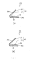
- Fig. 6 and Fig. 7 are a front view and a sectional view of an antenna unit according to the present invention, which is a third embodiment of the present invention, respectively, in a case where the antenna unit is placed in an electronic device.
- the electronic device 35 is configured by placing an antenna body 21 in a casing 36.
- the casing 36 has a power radiation conductor 37 that comprises a nearly rectangular metallic plate formed by performing e.g., printing, vapor deposition, laminating or plating of copper, copper alloy or aluminum. This power radiation conductor 37 is electrically isolated from the casing and the power supply conductor.
- the antenna body 21 is mounted on a printed circuit board 39 on which electronic parts comprising an RF control portion of the electronic device 35 are also mounted.
- the antenna body 21 is connected to the RF control portion 38 of the electronic device 35 through a transmission line (not shown) or the like. Further, the printed circuit board 39 is placed in the casing 36 of the electronic device 35.
- an antenna unit 40 consists of the antenna body 21 and the power radiation conductor 37 provided on the casing 36. Further, there is electromagnetic coupling between the power supply conductor 22 (Fig. 1), which is provided in the antenna body 21, and the power radiation conductor 37. Moreover, there is capacitance between the power radiation conductor 37 and the ground electrode (not shown). Consequently, the antenna unit comprises an antenna having a low resonance frequency.
- Fig. 8(a) and Fig. 8(b) are sectional views of first and second modifications of the antenna unit 40, which is the third embodiment of the present invention.
- the casing 36 of the electronic device 35 comprises a carrying case 36a and a cover 36b reclosably connected to the carrying case 36a. Further, a printed circuit board 39, on which an RF control portion 38 of the electronic device 35 is mounted, is provided in the carrying case 36a. Moreover, the antenna unit 21 is provided on the back surface of the cover 36b. The antenna unit 21 is connected to the RF control portion 38 of the electronic device 35 through a cable (not shown).
- the casing 36 of the electronic device 35 comprises a carrying case 36a and a cover 36b reclosably connected to the carrying case 36a. Further, a printed circuit board 39, on which an RF control portion 38 of the electronic device 35 is mounted, is provided in the carrying case 36a. Moreover, the antenna unit 21 is provided in the carrying case 36a. The power radiation conductor is provided on the cover 36b. The antenna unit 21 is connected to the RF control portion 31 of the electronic device 35 through a transmission line (not shown).
- the power radiation conductor 37 can be oriented in a position in which radio reception/transmission is optimum.
- FIGS. 8(a) and 8(b) illustrate the usage conditions of the electronic device.
- the electronic device is carried with the cover 36b disposed on the carrying case 36a. Further, the electronic device may be used with the cover 36b disposed down on the carrying case 36a. Moreover, the electronic device may be used with the cover 36b detached therefrom, by preliminarily putting the carrying case 36a and the cover 36b in a detachable state.
- FIGS. 6 to 8 illustrate the case that the power radiation conductor is placed in the casing 33 of the electronic device 35.
- the power radiation conductor 37 may be externally provided and added to the device 35 through a cable 41.
- the power radiation conductor 37 can be installed at a location where radio reception/transmission is optimum.
- a connector 41a may be attached to an end portion, which is at the side of the electronic device 35, of the cable 41.
- a connector (not shown) may be attached to the other end portion, which is at the side of the power radiation conductor 37, of the cable 41.
- connectors (not shown) may be attached to both of the end portions, which are at the sides of the electronic device 35 and the power radiation conductor 37, of the cable 41, respectively.
- the power radiation conductor 37 can be detached from the electronic device 35. Moreover, such electronic devices and antennas in these cases are convenient to carry.
- the antenna body 21 and the power radiation conductor 37 can be separated from each other in a range in which the electromagnetic coupling therebetween can be established.
- the power radiation conductor 37 can be oriented in a position wherein radio reception/transmission is optimum, by, for instance, attaching the power radiation conductor 37 to the casing 33 of the electronic device 35.
- the substrate of the antenna body comprises a dielectric material containing barium oxide, aluminum oxide and silica as major ingredients.
- the material of the substrate is not limited thereto.
- another dielectric material whose ingredients are titanium oxide and neodymium oxide, a magnetic material whose ingredients are nickel, cobalt and iron, or a combination of a dielectric material and a magnetic material may be employed as the material of the substrate of the antenna body.
- the antenna unit of the present invention responds to primary polarized waves, which come from the direction of the winding axis, and cross polarized waves which come from a direction perpendicular to the winding axis.
- the antenna unit of the present invention is a non-directional one.
- the antenna unit can have a plurality of resonance frequencies.
- the shape of the power radiation conductor is not limited to nearly rectangular. Further, similar advantages are obtained even if metallic foil or a mesh conductor is used instead of the metallic plate.
Landscapes
- Details Of Aerials (AREA)
- Support Of Aerials (AREA)
Claims (17)
- Eine Antenneneinheit, die folgende Merkmale aufweist:dadurch gekennzeichnet, daßeinen Antennenkörper (21), der ein Substrat (23) aufweist, wobei das Substrat eine erste Hauptoberfläche und eine Montageoberfläche (231) parallel zu der ersten Hauptoberfläche, und eine Seitenoberfläche, die die erste Hauptoberfläche und die Montageoberfläche (231) verbindet, aufweist, wobei das Substrat (23) zumindest ein dielektrisches Material oder ein magnetisches Material aufweist;zumindest einen Leistungsversorgungsleiter (22), der ein Leistungsversorgungsende (18a) und ein freies Ende (18b) aufweist;zumindest einen Leistungsversorgungsanschluß (19) zum Anlegen einer Spannung an das Leistungsversorgungsende (18a) des Leistungsversorgungsleiters (22); undeinen Leistungsabstrahlungsleiter (12; 37), der von dem Leistungsversorgungsleiter (22) elektrisch isoliert und mit diesem elektromagnetisch gekoppelt ist, wobei der Leistungsabstrahlungsleiter (12; 37) bei der ersten Hauptoberfläche angeordnet ist;der zumindest eine Leistungsversorgungsleiter (22) spiralförmig gewunden und in dem Substrat (23) angeordnet ist, wobei der spiralförmig gewundene Leiter (22) eine Spiralachse aufweist, die sich parallel zu der Montageoberfläche (231) erstreckt; undder zumindest eine Leistungsversorgungsanschluß (19) auf der Seitenoberfläche des Substrats (23) des Antennenkörpers (21) angeordnet ist.
- Die Antenneneinheit nach Anspruch 1, bei der der Leistungsabstrahlungsleiter (12; 37) bei einer elektronischen Vorrichtung (30; 35), auf der der Antennenkörper (21) montiert ist, oder bei dem Substrat (23) des Antennenkörpers (21) vorgesehen ist.
- Die Antenneneinheit nach einem beliebigen der Ansprüche 1 oder 2, bei der der Leistungsversorgungsleiter (22) eine im wesentlichen rechteckige Form in einem transversalen Querschnitt aufweist.
- Die Antenneneinheit nach einem beliebigen der Ansprüche 1 bis 3, bei der das Substrat (23) ein dielektrisches Material aufweist, das Bariumoxid, Aluminiumoxid und Siliziumdioxid aufweist.
- Die Antenneneinheit nach einem beliebigen der Ansprüche 1 bis 3, bei der das Substrat (23) ein dielektrisches Material aufweist, das Titanoxid und Neodymoxid aufweist.
- Die Antenneneinheit nach einem beliebigen der Ansprüche 1 bis 3, bei der das Substrat (23) ein magnetisches Material aufweist, das Nickel, Kobalt und Eisen aufweist.
- Die Antenneneinheit nach einem beliebigen der Ansprüche 1 bis 6, bei der das Substrat (23) eine Kombination eines dielektrischen Materials und eines magnetischen Materials aufweist.
- Die Antenneneinheit nach einem beliebigen der Ansprüche 1 bis 7, bei der der Leistungsabstrahlungsleiter (12) zumindest eine elektrisch leitende Platte, eine elektrisch leitende Folie oder eine elektrisch leitende Masche ist.
- Die Antenneneinheit nach einem beliebigen der Ansprüche 1 bis 8, bei der die Montageoberfläche (231) zum Montieren des Substrats auf eine Leiterplatte (32) dient.
- Die Antenneneinheit nach Anspruch 2, bei der der Leistungsabstrahlungsleiter (12) auf einem Gehäuse (33) der elektronischen Vorrichtung (30) vorgesehen ist.
- Die Antenneneinheit nach Anspruch 2, bei der das Substrat (23) auf einer Leiterplatte (32) der elektronischen Vorrichtung (30) montiert ist, wobei die elektronische Vorrichtung (30) einen Radiofrequenzsteuerabschnitt (31) aufweist, wobei der Leistungsversorgungsleiter (22) der Antenneneinheit (20; 40) mit dem Radiofrequenzsteuerabschnitt (31) über eine Übertragungsleitung verbunden ist.
- Die Antenneneinheit nach Anspruch 2, bei der die elektronische Vorrichtung (30) zwei Komponenten aufweist, einen Transportgehäuseabschnitt (33a; 36a), in dem der Radiofrequenzsteuerabschnitt (31) untergebracht ist, und einen Abdeckungsabschnitt (33b; 36b), wobei das Substrat (23), das den Leistungsversorgungsleiter (22) und den Leistungsabstrahlungsleiter (12) aufweist, in dem Abdeckungsabschnitt angeordnet.
- Die Antenneneinheit nach Anspruch 12, bei der der Abdeckungsabschnitt (33b; 36b) bezüglich des Transportgehäuseabschnitts (33a; 36a) bewegbar ist.
- Die Antenneneinheit nach Anspruch 12, bei der der Abdeckungsabschnitt (33b; 36b) von dem Transportgehäuseabschnitt (33a; 36a) abnehmbar ist.
- Die Antenneneinheit nach Anspruch 2, bei der die Antenneneinheit (20), die den Leistungsabstrahlungsleiter (12) und das Substrat (23) mit dem Leistungsversorgungsleiter (22) aufweist, bezüglich der elektronischen Vorrichtung (30; 35) bewegbar und mit der elektronischen Vorrichtung (30) durch ein Kabel (34) verbindbar ist.
- Die Antenneneinheit nach Anspruch 2, bei der der Leistungsabstrahlungsleiter (12) in dem Abdeckungsabschnitt (36b) angeordnet ist, und bei dem das Substrat (23), das den Leistungsversorgungsleiter (22) aufweist, in dem Transportgehäuseabschnitt (36a) mit dem Radiofrequenzsteuerabschnitt (31) angeordnet ist.
- Die Antenneneinheit nach Anspruch 2, bei der der Leistungsabstrahlungsleiter (12) von dem Substrat (23), das den Leistungsversorgungsleiter (22) aufweist, abnehmbar und mit der elektronischen Vorrichtung (30; 35) durch ein Kabel (34; 41) verbindbar ist.
Applications Claiming Priority (3)
| Application Number | Priority Date | Filing Date | Title |
|---|---|---|---|
| JP3377996 | 1996-02-21 | ||
| JP8033779A JP3055456B2 (ja) | 1996-02-21 | 1996-02-21 | アンテナ装置 |
| JP33779/96 | 1996-02-21 |
Publications (2)
| Publication Number | Publication Date |
|---|---|
| EP0793293A1 EP0793293A1 (de) | 1997-09-03 |
| EP0793293B1 true EP0793293B1 (de) | 2001-09-12 |
Family
ID=12395953
Family Applications (1)
| Application Number | Title | Priority Date | Filing Date |
|---|---|---|---|
| EP97102904A Expired - Lifetime EP0793293B1 (de) | 1996-02-21 | 1997-02-21 | Antenneneinheit |
Country Status (4)
| Country | Link |
|---|---|
| US (1) | US6054956A (de) |
| EP (1) | EP0793293B1 (de) |
| JP (1) | JP3055456B2 (de) |
| DE (1) | DE69706584T2 (de) |
Families Citing this family (14)
| Publication number | Priority date | Publication date | Assignee | Title |
|---|---|---|---|---|
| US6362790B1 (en) * | 1998-09-18 | 2002-03-26 | Tantivy Communications, Inc. | Antenna array structure stacked over printed wiring board with beamforming components |
| US6373436B1 (en) * | 1999-10-29 | 2002-04-16 | Qualcomm Incorporated | Dual strip antenna with periodic mesh pattern |
| US6653978B2 (en) * | 2000-04-20 | 2003-11-25 | Nokia Mobile Phones, Ltd. | Miniaturized radio frequency antenna |
| US6486853B2 (en) | 2000-05-18 | 2002-11-26 | Matsushita Electric Industrial Co., Ltd. | Chip antenna, radio communications terminal and radio communications system using the same and method for production of the same |
| JP2002100887A (ja) * | 2000-09-25 | 2002-04-05 | Toshiba Corp | 電子機器 |
| FR2825836B1 (fr) * | 2001-06-08 | 2005-09-23 | Centre Nat Rech Scient | Antenne resonante omnidirectionnelle |
| US7042418B2 (en) | 2002-11-27 | 2006-05-09 | Matsushita Electric Industrial Co., Ltd. | Chip antenna |
| FR2850189B1 (fr) * | 2003-01-16 | 2006-09-22 | Tagsys | Detecteur, systeme pour l'identification d'articles et procede de fabrication du detecteur |
| EP1593181A2 (de) | 2003-04-10 | 2005-11-09 | Matsushita Electric Industrial Co., Ltd. | Antennenelement, antennenmodul, und damit versehenes elektronisches gerät |
| WO2005022688A1 (en) * | 2003-09-01 | 2005-03-10 | Matsushita Electric Industrial Co., Ltd. | Antenna module |
| JP2005175757A (ja) * | 2003-12-10 | 2005-06-30 | Matsushita Electric Ind Co Ltd | アンテナモジュール |
| US7714795B2 (en) * | 2007-08-23 | 2010-05-11 | Research In Motion Limited | Multi-band antenna apparatus disposed on a three-dimensional substrate, and associated methodology, for a radio device |
| TW200929686A (en) * | 2007-12-31 | 2009-07-01 | High Tech Comp Corp | Antenna module, speaker and portable electronic device |
| JP6031970B2 (ja) * | 2012-11-26 | 2016-11-24 | 株式会社村田製作所 | アンテナコイル、部品内蔵基板および通信端末装置 |
Family Cites Families (10)
| Publication number | Priority date | Publication date | Assignee | Title |
|---|---|---|---|---|
| JPS5917705A (ja) * | 1982-07-22 | 1984-01-30 | Tdk Corp | 積層型平板アンテナコイル |
| GB2252452B (en) * | 1985-09-05 | 1992-12-16 | Plessey Co Plc | Improvements in or relating to hybrid structures |
| US4888597A (en) * | 1987-12-14 | 1989-12-19 | California Institute Of Technology | Millimeter and submillimeter wave antenna structure |
| JPH02214205A (ja) * | 1989-02-14 | 1990-08-27 | Fujitsu Ltd | 電子回路装置 |
| JPH0496520A (ja) * | 1990-08-13 | 1992-03-27 | Sharp Corp | データ送信装置 |
| JP2751683B2 (ja) * | 1991-09-11 | 1998-05-18 | 三菱電機株式会社 | 多層アレーアンテナ装置 |
| JPH0669057A (ja) * | 1992-08-19 | 1994-03-11 | Taiyo Yuden Co Ltd | 積層チップインダクタの製造方法 |
| JP3326935B2 (ja) * | 1993-12-27 | 2002-09-24 | 株式会社日立製作所 | 携帯無線機用小型アンテナ |
| US5450090A (en) * | 1994-07-20 | 1995-09-12 | The Charles Stark Draper Laboratory, Inc. | Multilayer miniaturized microstrip antenna |
| US5649306A (en) * | 1994-09-16 | 1997-07-15 | Motorola, Inc. | Portable radio housing incorporating diversity antenna structure |
-
1996
- 1996-02-21 JP JP8033779A patent/JP3055456B2/ja not_active Expired - Lifetime
-
1997
- 1997-02-21 US US08/803,626 patent/US6054956A/en not_active Expired - Lifetime
- 1997-02-21 EP EP97102904A patent/EP0793293B1/de not_active Expired - Lifetime
- 1997-02-21 DE DE69706584T patent/DE69706584T2/de not_active Expired - Lifetime
Also Published As
| Publication number | Publication date |
|---|---|
| DE69706584T2 (de) | 2002-08-22 |
| US6054956A (en) | 2000-04-25 |
| JPH09232828A (ja) | 1997-09-05 |
| EP0793293A1 (de) | 1997-09-03 |
| JP3055456B2 (ja) | 2000-06-26 |
| DE69706584D1 (de) | 2001-10-18 |
Similar Documents
| Publication | Publication Date | Title |
|---|---|---|
| US6271803B1 (en) | Chip antenna and radio equipment including the same | |
| US6603430B1 (en) | Handheld wireless communication devices with antenna having parasitic element | |
| EP1170822B1 (de) | Adapter-Antenne für Mobiltelephone | |
| JP3166589B2 (ja) | チップアンテナ | |
| US6329950B1 (en) | Planar antenna comprising two joined conducting regions with coax | |
| EP0648023B1 (de) | Tragbares Funkgerät mit Diversityempfänger | |
| EP0793293B1 (de) | Antenneneinheit | |
| EP0339628A2 (de) | Abnehmbarer Batterieblock mit einer eingebauten Breitband-Antenne | |
| WO2002063713A2 (en) | Notch antennas and wireless communicators incorporating same | |
| WO2001063695A1 (en) | Compact, broadband inverted-f antennas with conductive elements and wireless communicators incorporating same | |
| EP1360739A1 (de) | Antennensystem mit gekoppelten internen pifa und einziehbaren antennen und drahtlose kommunikationsgeräte mit derartigem antennensystem | |
| US5541616A (en) | Surface-mountable antenna | |
| EP0740362B1 (de) | Breitbandige ebene Antenne mit hohem Gewinn | |
| US20060290575A1 (en) | Antenna integrated into a housing | |
| JP3305487B2 (ja) | 通信機 | |
| EP0828310B1 (de) | Antennenvorrichtung | |
| US20020123312A1 (en) | Antenna systems including internal planar inverted-F Antenna coupled with external radiating element and wireless communicators incorporating same | |
| JPH11340726A (ja) | アンテナ装置 | |
| EP0929116B1 (de) | Antenne | |
| US5428362A (en) | Substrate integrated antenna | |
| WO2024259969A1 (zh) | 天线组件、通信设备及车辆 | |
| JP3006399B2 (ja) | デュアルバンドアンテナ | |
| WO2008032886A1 (en) | Antenna for wireless communication and method of fabricating the same | |
| CN119275582B (zh) | 双频天线和通信设备 | |
| JP3237604B2 (ja) | アンテナ装置 |
Legal Events
| Date | Code | Title | Description |
|---|---|---|---|
| PUAI | Public reference made under article 153(3) epc to a published international application that has entered the european phase |
Free format text: ORIGINAL CODE: 0009012 |
|
| 17P | Request for examination filed |
Effective date: 19970221 |
|
| AK | Designated contracting states |
Kind code of ref document: A1 Designated state(s): DE FR GB |
|
| 17Q | First examination report despatched |
Effective date: 19981112 |
|
| GRAG | Despatch of communication of intention to grant |
Free format text: ORIGINAL CODE: EPIDOS AGRA |
|
| GRAG | Despatch of communication of intention to grant |
Free format text: ORIGINAL CODE: EPIDOS AGRA |
|
| GRAH | Despatch of communication of intention to grant a patent |
Free format text: ORIGINAL CODE: EPIDOS IGRA |
|
| GRAH | Despatch of communication of intention to grant a patent |
Free format text: ORIGINAL CODE: EPIDOS IGRA |
|
| GRAA | (expected) grant |
Free format text: ORIGINAL CODE: 0009210 |
|
| AK | Designated contracting states |
Kind code of ref document: B1 Designated state(s): DE FR GB |
|
| REF | Corresponds to: |
Ref document number: 69706584 Country of ref document: DE Date of ref document: 20011018 |
|
| ET | Fr: translation filed | ||
| REG | Reference to a national code |
Ref country code: GB Ref legal event code: IF02 |
|
| PLBE | No opposition filed within time limit |
Free format text: ORIGINAL CODE: 0009261 |
|
| STAA | Information on the status of an ep patent application or granted ep patent |
Free format text: STATUS: NO OPPOSITION FILED WITHIN TIME LIMIT |
|
| 26N | No opposition filed | ||
| REG | Reference to a national code |
Ref country code: FR Ref legal event code: PLFP Year of fee payment: 20 |
|
| PGFP | Annual fee paid to national office [announced via postgrant information from national office to epo] |
Ref country code: DE Payment date: 20160218 Year of fee payment: 20 |
|
| PGFP | Annual fee paid to national office [announced via postgrant information from national office to epo] |
Ref country code: GB Payment date: 20160217 Year of fee payment: 20 Ref country code: FR Payment date: 20160218 Year of fee payment: 20 |
|
| REG | Reference to a national code |
Ref country code: DE Ref legal event code: R071 Ref document number: 69706584 Country of ref document: DE |
|
| REG | Reference to a national code |
Ref country code: GB Ref legal event code: PE20 Expiry date: 20170220 |
|
| PG25 | Lapsed in a contracting state [announced via postgrant information from national office to epo] |
Ref country code: GB Free format text: LAPSE BECAUSE OF EXPIRATION OF PROTECTION Effective date: 20170220 |