EP0792506B1 - Refresh strategy for drams - Google Patents
Refresh strategy for drams Download PDFInfo
- Publication number
- EP0792506B1 EP0792506B1 EP96922577A EP96922577A EP0792506B1 EP 0792506 B1 EP0792506 B1 EP 0792506B1 EP 96922577 A EP96922577 A EP 96922577A EP 96922577 A EP96922577 A EP 96922577A EP 0792506 B1 EP0792506 B1 EP 0792506B1
- Authority
- EP
- European Patent Office
- Prior art keywords
- refresh
- memory bank
- memory
- refreshing
- banks
- Prior art date
- Legal status (The legal status is an assumption and is not a legal conclusion. Google has not performed a legal analysis and makes no representation as to the accuracy of the status listed.)
- Expired - Lifetime
Links
Images
Classifications
-
- G—PHYSICS
- G11—INFORMATION STORAGE
- G11C—STATIC STORES
- G11C11/00—Digital stores characterised by the use of particular electric or magnetic storage elements; Storage elements therefor
- G11C11/21—Digital stores characterised by the use of particular electric or magnetic storage elements; Storage elements therefor using electric elements
- G11C11/34—Digital stores characterised by the use of particular electric or magnetic storage elements; Storage elements therefor using electric elements using semiconductor devices
- G11C11/40—Digital stores characterised by the use of particular electric or magnetic storage elements; Storage elements therefor using electric elements using semiconductor devices using transistors
- G11C11/401—Digital stores characterised by the use of particular electric or magnetic storage elements; Storage elements therefor using electric elements using semiconductor devices using transistors forming cells needing refreshing or charge regeneration, i.e. dynamic cells
- G11C11/4063—Auxiliary circuits, e.g. for addressing, decoding, driving, writing, sensing or timing
- G11C11/407—Auxiliary circuits, e.g. for addressing, decoding, driving, writing, sensing or timing for memory cells of the field-effect type
- G11C11/408—Address circuits
-
- G—PHYSICS
- G11—INFORMATION STORAGE
- G11C—STATIC STORES
- G11C11/00—Digital stores characterised by the use of particular electric or magnetic storage elements; Storage elements therefor
- G11C11/21—Digital stores characterised by the use of particular electric or magnetic storage elements; Storage elements therefor using electric elements
- G11C11/34—Digital stores characterised by the use of particular electric or magnetic storage elements; Storage elements therefor using electric elements using semiconductor devices
- G11C11/40—Digital stores characterised by the use of particular electric or magnetic storage elements; Storage elements therefor using electric elements using semiconductor devices using transistors
- G11C11/401—Digital stores characterised by the use of particular electric or magnetic storage elements; Storage elements therefor using electric elements using semiconductor devices using transistors forming cells needing refreshing or charge regeneration, i.e. dynamic cells
- G11C11/406—Management or control of the refreshing or charge-regeneration cycles
Definitions
- the present invention relates to a method of refreshing memory cells within a dynamic random access memory (DRAM), and in particular, to a method which reduces the refresh noise on the drain voltage of a DRAM using CMOS.
- DRAM dynamic random access memory
- dynamic random access memories require periodic refreshing of the memory cells within the DRAM so that the data stored within each memory cell does not corrupt or decay over time.
- refreshing is an essential element of memory storage for volatile memories.
- a refresh may be a CAS (column address select) before RAS (row address select) refresh, or a RAS-only refresh.
- a CAS before RAS refresh involves asserting the CAS signal before the RAS signal is asserted to indicate that the next cycle is a refresh cycle.
- an internal address counter in the memory supplies the row address of the next row to be refreshed.
- a RAS-only refresh operates in a similar manner to refresh selected rows of memory; however, the address of the row to be refreshed is instead supplied by an external refresh circuit.
- previous refresh methods have contemplated staggering refreshes applied to adjacent single in-line memory modules (SIMMS) so that the refreshes occur one after the other and are separated by at least one clock cycle.
- SIMMS single in-line memory modules
- filtering capacitors are provided for each memory bank to hold the line voltage up during a high current draw.
- this approach serves to distribute the voltage drop produced during a refresh evenly over multiple clock cycles, voltage drop reduction is still not optimized. This is because sometimes adjacent memory banks share one or more filtering capacitors so that if, for example, the first and second memory banks are refreshed in sequence, the filtering capacitors do not have sufficient recovery time to recharge to the nominal line voltage.
- memory banks sharing the same filtering capacitor are refreshed in consecutive clock cycles, there is a possibility that a significant voltage drop wilt be observed on the voltage supply line connected to the accessed memory banks and that the resulting noise will affect the operation of the DRAMS.
- a method for refreshing volatile memory banks is characterised by the steps defined in claim 1.
- the first, second and third memory banks are CMOS memory banks.
- the method includes the step of initiating a refresh of a fourth memory bank subsequent to initiating the refresh of the second memory bank, wherein the fourth memory bank and the third memory bank share another filtering capacitance.
- the method includes the refreshing of the third memory bank and refreshing of at least one additional memory bank between the refreshing of the first memory bank and the refreshing of the second memory bank.
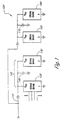
- Figure 1 is schematic block diagram which illustrates two pair of memory banks which each share a filtering capacitor.
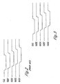
- Figure 2 is a timing diagram which illustrates the order of refresh accesses to each of the memory banks as performed in accordance with the method of the prior art.
- Figure 3 is a timing diagram which illustrates the order of refresh accesses to the memory banks of Figure 1 in accordance with the method of the present invention.
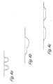
- Figures 4A through 4C are signal diagrams which illustrate the voltage drop which occurs during a refresh for the case where (A) a staggered method of the prior art is used to access adjacent memory banks where no filtering capacitor is used; (B) the method of the prior art is used to refresh adjacent memory banks sharing the same filtering capacitors; and (C) the method of the present invention is used to access adjacent memory banks at spaced intervals where the filtering capacitor is shared between the memory banks.
- FIG. 1 is a simplified schematic block diagram which illustrates a plurality of dynamic random accessory memory (DRAM) banks 100 in connection with a voltage supply line 110.
- DRAM dynamic random accessory memory
- a first DRAM bank 120 and a second DRAM bank 130 share a filtering capacitor bank 140.
- the capacitor bank 140 may comprise a plurality of capacitors shared by each of the DRAM elements within the DRAM banks 120, 130.
- a third DRAM bank 150 and a fourth DRAM bank 160 share a capacitor bank 170.
- refreshes of the memory cells within each of the DRAM banks 120, 130, 150 and 160 are performed in a predetermined order so as to reduce the instantaneous current drain via the line 110.
- the voltage supply line 110 includes some impedance so that when a sudden current draw occurs at some point along the line 110, it is possible that a significant voltage drop will be observed at that location of the line 110.
- the filtering capacitors 140, 170 are included at a number of locations along the voltage source line 110 to alleviate the effects of such a voltage draw.
- the refresh accesses which are often responsible for sudden current draws on the line 110 are staggered to reduce the total current draw at any given place along the line 110.
- Figure 4A shows the voltage drop which would be observed along the line 110 at the DRAM banks 120, 130 if the RAS 2 signal is asserted immediately after the RAS 1 signal (as shown in Figure 2), while no filtering capacitor 140 is present.
- Figure 4A illustrates the close proximity of the voltage drops observed at the voltage inputs to the memory banks 120, 130 when these adjacent memory banks are refreshed in consecutive clock cycles.
- the voltage drop observed is represented as shown in Figure 4B.
- the voltage drop observed at the voltage supply inputs to the DRAM banks 120, 130 is not as severe as the voltage drop which would be observed if the capacitor 140 were not present at the first voltage drop, when the second voltage drop occurs while the voltage on the line 110 near the DRAM banks 120, 130 has not yet recovered to its original value, a large drop is observed upon the assertion of the second row address strobe signal.
- the method of the prior art results in a significant voltage drop to the voltage supply inputs of adjacent DRAM banks if the refreshes occur in rapid succession so that the filtering capacitor 140 does not have time to recover from the original voltage drop.
- This problem is further exacerbated if the DRAM banks 120, 130 employ CMOS technology, because CMOS technology is particularly susceptible to noise in the presence of such voltage drops.
- FIG. 3 an unproved method of accessing DRAM banks during refreshes is illustrated in Figure 3.
- the sequence of DRAM refreshes is altered so that DRAM banks sharing the same filtering capacitors are not accessed in consecutive clock cycles. That is, as shown in Figure 3, the row address strobe used to refresh the second DRAM bank 130 is asserted, followed by the row address strobe signal used to refresh the fourth DRAM bank 160, followed by the row address strobe signal used to refresh the first DRAM bank 120, and, finally, the row address strobe signal used to refresh the third DRAM bank 150 is asserted.
- the row address strobe signal used to refresh the third DRAM bank 150 is asserted.
Landscapes
- Engineering & Computer Science (AREA)
- Microelectronics & Electronic Packaging (AREA)
- Computer Hardware Design (AREA)
- Dram (AREA)
Applications Claiming Priority (3)
| Application Number | Priority Date | Filing Date | Title |
|---|---|---|---|
| US527950 | 1995-09-14 | ||
| US08/527,950 US5654929A (en) | 1995-09-14 | 1995-09-14 | Refresh strategy for DRAMs |
| PCT/US1996/010854 WO1997010601A1 (en) | 1995-09-14 | 1996-06-27 | Refresh strategy for drams |
Publications (3)
| Publication Number | Publication Date |
|---|---|
| EP0792506A1 EP0792506A1 (en) | 1997-09-03 |
| EP0792506A4 EP0792506A4 (en) | 1998-08-19 |
| EP0792506B1 true EP0792506B1 (en) | 2002-05-29 |
Family
ID=24103635
Family Applications (1)
| Application Number | Title | Priority Date | Filing Date |
|---|---|---|---|
| EP96922577A Expired - Lifetime EP0792506B1 (en) | 1995-09-14 | 1996-06-27 | Refresh strategy for drams |
Country Status (12)
| Country | Link |
|---|---|
| US (1) | US5654929A (ca) |
| EP (1) | EP0792506B1 (ca) |
| JP (1) | JP4166274B2 (ca) |
| KR (1) | KR100248259B1 (ca) |
| CN (1) | CN1130730C (ca) |
| AU (1) | AU6393496A (ca) |
| DE (1) | DE69621419T2 (ca) |
| FI (1) | FI113572B (ca) |
| IN (1) | IN192635B (ca) |
| RU (1) | RU2163035C2 (ca) |
| TW (1) | TW303469B (ca) |
| WO (2) | WO1997010602A1 (ca) |
Families Citing this family (34)
| Publication number | Priority date | Publication date | Assignee | Title |
|---|---|---|---|---|
| US6610493B1 (en) | 1993-06-17 | 2003-08-26 | Brigham And Women's Hospital | Screening compounds for the ability to alter the production of amyloid-β peptide |
| US5841686A (en) * | 1996-11-22 | 1998-11-24 | Ma Laboratories, Inc. | Dual-bank memory module with shared capacitors and R-C elements integrated into the module substrate |
| KR100243335B1 (ko) * | 1996-12-31 | 2000-02-01 | 김영환 | 독립적인 리프레쉬 수단을 가지는 데이지 체인 구조의 반도체 장치 |
| DE19855445C1 (de) * | 1998-12-01 | 2000-02-24 | Siemens Ag | Vorrichtung zur Verringerung der elektromagnetischen Emission bei integrierten Schaltungen mit Treiberstufen |
| JP4270707B2 (ja) * | 1999-04-09 | 2009-06-03 | 株式会社東芝 | ダイナミック型半導体記憶装置 |
| US7124285B2 (en) * | 2001-03-29 | 2006-10-17 | Intel Corporation | Peak power reduction when updating future file |
| US6532175B1 (en) * | 2002-01-16 | 2003-03-11 | Advanced Micro Devices, In. | Method and apparatus for soft program verification in a memory device |
| CN101042933B (zh) * | 2007-04-12 | 2010-05-19 | 复旦大学 | 非挥发sram单元、阵列及其操作方法和应用 |
| CN101504865B (zh) * | 2009-03-06 | 2011-06-22 | 成都市华为赛门铁克科技有限公司 | 存储系统的数据处理方法及存储设备 |
| JP6314673B2 (ja) * | 2014-06-11 | 2018-04-25 | 富士電機株式会社 | 半導体装置 |
| KR20160013624A (ko) * | 2014-07-28 | 2016-02-05 | 에스케이하이닉스 주식회사 | 리프레쉬 회로 |
| US10490251B2 (en) | 2017-01-30 | 2019-11-26 | Micron Technology, Inc. | Apparatuses and methods for distributing row hammer refresh events across a memory device |
| KR20190075341A (ko) | 2017-12-21 | 2019-07-01 | 에스케이하이닉스 주식회사 | 반도체 메모리 장치 |
| US11200944B2 (en) | 2017-12-21 | 2021-12-14 | SK Hynix Inc. | Semiconductor memory apparatus operating in a refresh mode and method for performing the same |
| WO2019222960A1 (en) | 2018-05-24 | 2019-11-28 | Micron Technology, Inc. | Apparatuses and methods for pure-time, self adopt sampling for row hammer refresh sampling |
| US10573370B2 (en) | 2018-07-02 | 2020-02-25 | Micron Technology, Inc. | Apparatus and methods for triggering row hammer address sampling |
| US10685696B2 (en) | 2018-10-31 | 2020-06-16 | Micron Technology, Inc. | Apparatuses and methods for access based refresh timing |
| CN113168861B (zh) | 2018-12-03 | 2024-05-14 | 美光科技公司 | 执行行锤刷新操作的半导体装置 |
| CN117198356A (zh) | 2018-12-21 | 2023-12-08 | 美光科技公司 | 用于目标刷新操作的时序交错的设备和方法 |
| US10957377B2 (en) | 2018-12-26 | 2021-03-23 | Micron Technology, Inc. | Apparatuses and methods for distributed targeted refresh operations |
| US11615831B2 (en) * | 2019-02-26 | 2023-03-28 | Micron Technology, Inc. | Apparatuses and methods for memory mat refresh sequencing |
| US11227649B2 (en) | 2019-04-04 | 2022-01-18 | Micron Technology, Inc. | Apparatuses and methods for staggered timing of targeted refresh operations |
| US11069393B2 (en) | 2019-06-04 | 2021-07-20 | Micron Technology, Inc. | Apparatuses and methods for controlling steal rates |
| US10978132B2 (en) | 2019-06-05 | 2021-04-13 | Micron Technology, Inc. | Apparatuses and methods for staggered timing of skipped refresh operations |
| US11302374B2 (en) | 2019-08-23 | 2022-04-12 | Micron Technology, Inc. | Apparatuses and methods for dynamic refresh allocation |
| US11302377B2 (en) | 2019-10-16 | 2022-04-12 | Micron Technology, Inc. | Apparatuses and methods for dynamic targeted refresh steals |
| US11309010B2 (en) | 2020-08-14 | 2022-04-19 | Micron Technology, Inc. | Apparatuses, systems, and methods for memory directed access pause |
| US11380382B2 (en) | 2020-08-19 | 2022-07-05 | Micron Technology, Inc. | Refresh logic circuit layout having aggressor detector circuit sampling circuit and row hammer refresh control circuit |
| US11348631B2 (en) | 2020-08-19 | 2022-05-31 | Micron Technology, Inc. | Apparatuses, systems, and methods for identifying victim rows in a memory device which cannot be simultaneously refreshed |
| US11557331B2 (en) | 2020-09-23 | 2023-01-17 | Micron Technology, Inc. | Apparatuses and methods for controlling refresh operations |
| US11222686B1 (en) | 2020-11-12 | 2022-01-11 | Micron Technology, Inc. | Apparatuses and methods for controlling refresh timing |
| US11264079B1 (en) | 2020-12-18 | 2022-03-01 | Micron Technology, Inc. | Apparatuses and methods for row hammer based cache lockdown |
| US12125514B2 (en) | 2022-04-28 | 2024-10-22 | Micron Technology, Inc. | Apparatuses and methods for access based refresh operations |
| US12112787B2 (en) | 2022-04-28 | 2024-10-08 | Micron Technology, Inc. | Apparatuses and methods for access based targeted refresh operations |
Family Cites Families (4)
| Publication number | Priority date | Publication date | Assignee | Title |
|---|---|---|---|---|
| US4887240A (en) * | 1987-12-15 | 1989-12-12 | National Semiconductor Corporation | Staggered refresh for dram array |
| US5113372A (en) * | 1990-06-06 | 1992-05-12 | Micron Technology, Inc. | Actively controlled transient reducing current supply and regulation circuits for random access memory integrated circuits |
| JPH06338187A (ja) * | 1993-05-27 | 1994-12-06 | Melco:Kk | Dramを用いたメモリ装置 |
| US5465237A (en) * | 1994-12-01 | 1995-11-07 | Advanced Peripherals Labs, Inc. | RAS encoded generator for a memory bank |
-
1995
- 1995-09-14 US US08/527,950 patent/US5654929A/en not_active Expired - Lifetime
-
1996
- 1996-06-27 CN CN96191400A patent/CN1130730C/zh not_active Expired - Lifetime
- 1996-06-27 EP EP96922577A patent/EP0792506B1/en not_active Expired - Lifetime
- 1996-06-27 JP JP51068697A patent/JP4166274B2/ja not_active Expired - Fee Related
- 1996-06-27 RU RU97110100/09A patent/RU2163035C2/ru not_active IP Right Cessation
- 1996-06-27 KR KR1019970703236A patent/KR100248259B1/ko not_active Expired - Fee Related
- 1996-06-27 AU AU63934/96A patent/AU6393496A/en not_active Abandoned
- 1996-06-27 WO PCT/US1996/010855 patent/WO1997010602A1/en not_active Ceased
- 1996-06-27 WO PCT/US1996/010854 patent/WO1997010601A1/en not_active Ceased
- 1996-06-27 DE DE69621419T patent/DE69621419T2/de not_active Expired - Lifetime
- 1996-07-03 IN IN1173MA1996 patent/IN192635B/en unknown
- 1996-07-20 TW TW085108858A patent/TW303469B/zh not_active IP Right Cessation
-
1997
- 1997-05-14 FI FI972050A patent/FI113572B/fi not_active IP Right Cessation
Also Published As
| Publication number | Publication date |
|---|---|
| WO1997010602A1 (en) | 1997-03-20 |
| KR970707554A (ko) | 1997-12-01 |
| EP0792506A1 (en) | 1997-09-03 |
| IN192635B (ca) | 2004-05-08 |
| DE69621419D1 (de) | 2002-07-04 |
| CN1130730C (zh) | 2003-12-10 |
| JPH10509269A (ja) | 1998-09-08 |
| KR100248259B1 (ko) | 2000-03-15 |
| WO1997010601A1 (en) | 1997-03-20 |
| DE69621419T2 (de) | 2003-01-16 |
| CN1169205A (zh) | 1997-12-31 |
| AU6393496A (en) | 1997-04-01 |
| FI972050A0 (fi) | 1997-05-14 |
| JP4166274B2 (ja) | 2008-10-15 |
| EP0792506A4 (en) | 1998-08-19 |
| FI113572B (fi) | 2004-05-14 |
| TW303469B (ca) | 1997-04-21 |
| FI972050L (fi) | 1997-05-14 |
| US5654929A (en) | 1997-08-05 |
| RU2163035C2 (ru) | 2001-02-10 |
Similar Documents
| Publication | Publication Date | Title |
|---|---|---|
| EP0792506B1 (en) | Refresh strategy for drams | |
| US4887240A (en) | Staggered refresh for dram array | |
| US6721222B2 (en) | Noise suppression for open bit line DRAM architectures | |
| US10049716B2 (en) | Refresh request queuing circuitry | |
| US7349277B2 (en) | Method and system for reducing the peak current in refreshing dynamic random access memory devices | |
| US5802395A (en) | High density memory modules with improved data bus performance | |
| US5251178A (en) | Low-power integrated circuit memory | |
| US5305274A (en) | Method and apparatus for refreshing a dynamic random access memory | |
| US5333128A (en) | Semiconductor memory device having a circuit for reducing frequency of proceeding refresh in data retention mode | |
| DE102004044984B4 (de) | Direktzugriffspeichervorrichtung, Halbleiterspeichervorrichtung und Verfahren zum Verringern eines Stromverbrauchs bei einer dynamischen Speichervorrichtung | |
| US5434816A (en) | Two-transistor dynamic random-access memory cell having a common read/write terminal | |
| US6646941B1 (en) | Apparatus for operating an integrated circuit having a sleep mode | |
| EP0811984B1 (de) | Verfahren zum Lesen und Auffrischen eines dynamischen Halbleiterspeichers | |
| US7120077B2 (en) | Memory module having a plurality of integrated memory components | |
| EP1540658B1 (en) | Refreshing of multi-port memory in integrated circuits | |
| US11238916B2 (en) | Method for refreshing a memory device, in which the victim row refresh operation is hidden in the normal refresh operation without affecting the time allocated for the normal refresh operation | |
| DE19807014A1 (de) | Halbleiterspeicherelement mit verbesserter Datenausgabegeschwindigkeit | |
| EP4369341A1 (en) | Integrated dram circuit, method for refreshing memory cells, and method for preventing a data integrity attack | |
| HK90897A (en) | Circuitry for the on-chip interleaved access to dynamic ram modules | |
| KR20020042030A (ko) | 리프레쉬 수행시간이 감소될 수 있는 다중 뱅크를구비하는 반도체 메모리 장치 및 리프레쉬 방법 | |
| US20050088894A1 (en) | Auto-refresh multiple row activation | |
| JPH01227299A (ja) | メモリのリフレッシュ制御方式 | |
| DE102006040399A1 (de) | Vorrichtung zur Erneuerung von Speicherinhalten | |
| US6839294B2 (en) | Memory device with high charging voltage bit line | |
| WO1994012934A1 (en) | Alternate dram refresh controlled by signal period detector |
Legal Events
| Date | Code | Title | Description |
|---|---|---|---|
| PUAI | Public reference made under article 153(3) epc to a published international application that has entered the european phase |
Free format text: ORIGINAL CODE: 0009012 |
|
| AK | Designated contracting states |
Kind code of ref document: A1 Designated state(s): DE FR GB IT |
|
| 17P | Request for examination filed |
Effective date: 19970917 |
|
| A4 | Supplementary search report drawn up and despatched |
Effective date: 19980629 |
|
| AK | Designated contracting states |
Kind code of ref document: A4 Designated state(s): DE FR GB IT |
|
| 17Q | First examination report despatched |
Effective date: 20000516 |
|
| GRAG | Despatch of communication of intention to grant |
Free format text: ORIGINAL CODE: EPIDOS AGRA |
|
| GRAG | Despatch of communication of intention to grant |
Free format text: ORIGINAL CODE: EPIDOS AGRA |
|
| GRAH | Despatch of communication of intention to grant a patent |
Free format text: ORIGINAL CODE: EPIDOS IGRA |
|
| GRAH | Despatch of communication of intention to grant a patent |
Free format text: ORIGINAL CODE: EPIDOS IGRA |
|
| GRAA | (expected) grant |
Free format text: ORIGINAL CODE: 0009210 |
|
| AK | Designated contracting states |
Kind code of ref document: B1 Designated state(s): DE FR GB IT |
|
| REG | Reference to a national code |
Ref country code: GB Ref legal event code: FG4D |
|
| REF | Corresponds to: |
Ref document number: 69621419 Country of ref document: DE Date of ref document: 20020704 |
|
| ET | Fr: translation filed | ||
| PLBE | No opposition filed within time limit |
Free format text: ORIGINAL CODE: 0009261 |
|
| STAA | Information on the status of an ep patent application or granted ep patent |
Free format text: STATUS: NO OPPOSITION FILED WITHIN TIME LIMIT |
|
| 26N | No opposition filed |
Effective date: 20030303 |
|
| PGFP | Annual fee paid to national office [announced via postgrant information from national office to epo] |
Ref country code: DE Payment date: 20120524 Year of fee payment: 17 |
|
| PGFP | Annual fee paid to national office [announced via postgrant information from national office to epo] |
Ref country code: GB Payment date: 20120525 Year of fee payment: 17 Ref country code: FR Payment date: 20120705 Year of fee payment: 17 |
|
| PGFP | Annual fee paid to national office [announced via postgrant information from national office to epo] |
Ref country code: IT Payment date: 20120526 Year of fee payment: 17 |
|
| GBPC | Gb: european patent ceased through non-payment of renewal fee |
Effective date: 20130627 |
|
| REG | Reference to a national code |
Ref country code: DE Ref legal event code: R119 Ref document number: 69621419 Country of ref document: DE Effective date: 20140101 |
|
| REG | Reference to a national code |
Ref country code: FR Ref legal event code: ST Effective date: 20140228 |
|
| PG25 | Lapsed in a contracting state [announced via postgrant information from national office to epo] |
Ref country code: GB Free format text: LAPSE BECAUSE OF NON-PAYMENT OF DUE FEES Effective date: 20130627 Ref country code: DE Free format text: LAPSE BECAUSE OF NON-PAYMENT OF DUE FEES Effective date: 20140101 |
|
| PG25 | Lapsed in a contracting state [announced via postgrant information from national office to epo] |
Ref country code: IT Free format text: LAPSE BECAUSE OF NON-PAYMENT OF DUE FEES Effective date: 20130627 Ref country code: FR Free format text: LAPSE BECAUSE OF NON-PAYMENT OF DUE FEES Effective date: 20130701 |